

Page 1

INTEGRATED CIRCUITS
DATA SH EET
For a complete data sheet, please also download:
•The IC06 74HC/HCT/HCU/HCMOS Logic Family Specifications
•The IC06 74HC/HCT/HCU/HCMOS Logic Package Information
•The IC06 74HC/HCT/HCU/HCMOS Logic Package Outlines
74HC/HCT03
Quad 2-input NAND gate
Product specification
File under Integrated Circuits, IC06
December 1990
Page 2

Philips Semiconductors Product specification
Quad 2-input NAND gate 74HC/HCT03
FEATURES
• Level shift capability
• Output capability: standard (open drain)
• ICC category: SSI
The 74HC/HCT03 provide the 2-input NAND function.
The 74HC/HCT03 have open-drain N-transistor outputs,
which are not clamped by a diode connected to V
the OFF-state, i.e. when one input is LOW, the output
may be pulled to any voltage between GND and V
This allows the device to be used as a LOW-to-HIGH or
GENERAL DESCRIPTION
HIGH-to-LOW level shifter. For digital operation and
OR-tied output applications, these devices must have a
The 74HC/HCT03 are high-speed Si-gate CMOS devices
pull-up resistor to establish a logic HIGH level.
and are pin compatible with low power Schottky TTL
(LSTTL). They are specified in compliance with JEDEC
standard no. 7A.
QUICK REFERENCE DATA
GND = 0 V; T
=25°C; tr=tf= 6 ns
amb
SYMBOL PARAMETER CONDITIONS
t
C
C
PZL
I
PD
/ t
PLZ
propagation delay CL= 15 pF; RL=1 kΩ; VCC= 5 V 8 10 ns
input capacitance 3.5 3.5 pF
power dissipation capacitance per gate notes 1, 2 and 3 4.0 4.0 pF
Notes
1. C
is used to determine the dynamic power dissipation (PD in µW):
PD
TYPICAL
HC HCT
. In
CC
Omax
UNIT
.
PD=CPD × V
2
× fi+ ∑ (CL× V
CC
2
× fo) + ∑ (V
CC
fi= input frequency in MHz
fo= output frequency in MHz
VO= output voltage in V
CL= output load capacitance in pF
VCC= supply voltage in V
RL= pull-up resistor in MΩ
∑ (CL× V
∑ (V
O
2. For HC the condition is VI= GND to V
2
× fo) = sum of outputs
CC
2
/RL) = sum of outputs
CC
For HCT the condition is VI= GND to VCC− 1.5 V
3. The given value of CPD is obtained with:
CL= 0 pF and RL= ∞
ORDERING INFORMATION
“74HC/HCT/HCU/HCMOS Logic Package Information”
See
2
/RL) × duty factor LOW, where:
O
.
December 1990 2
Page 3
Philips Semiconductors Product specification
Quad 2-input NAND gate 74HC/HCT03
PIN DESCRIPTION
PIN NO. SYMBOL NAME AND FUNCTION
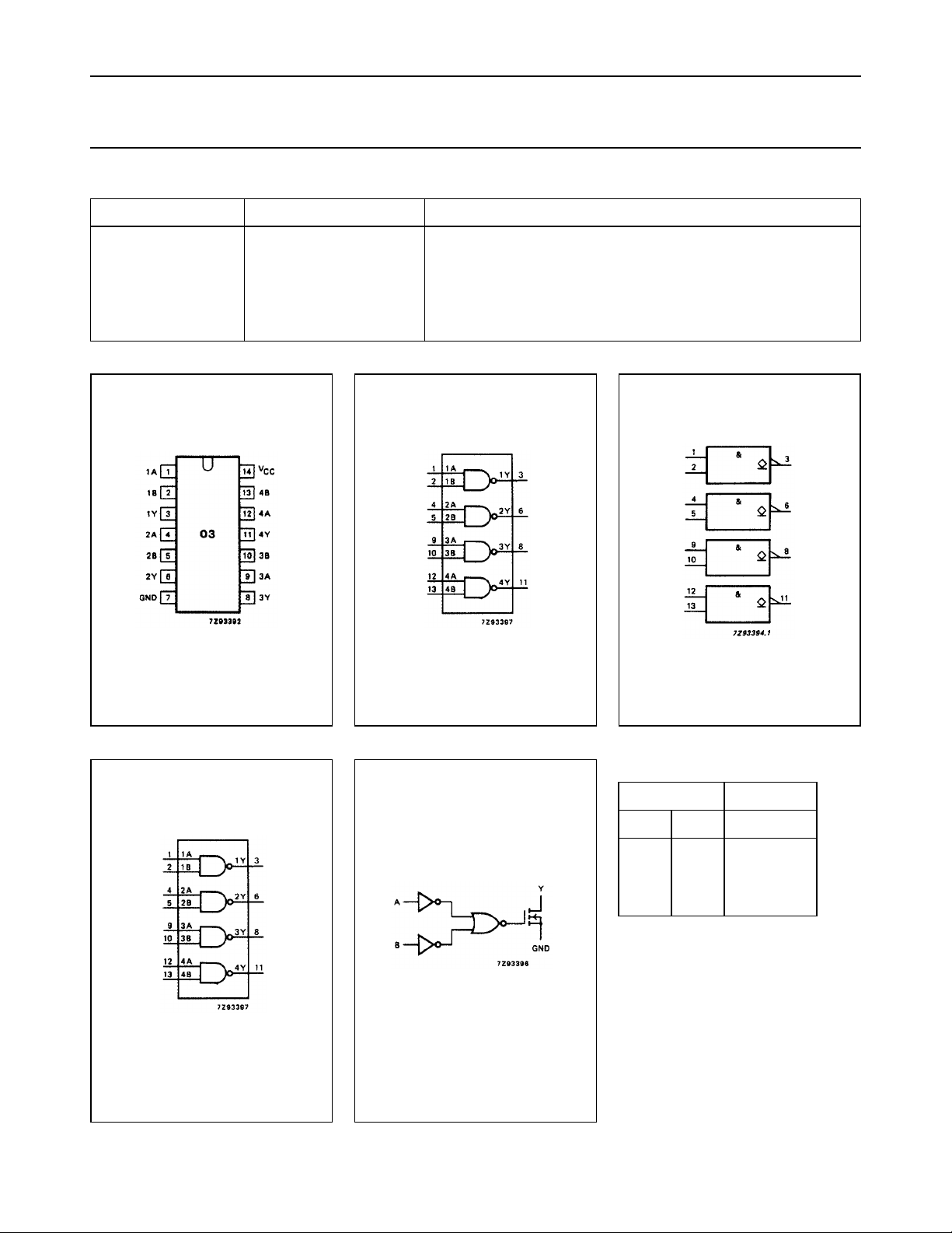
1, 4, 9, 12 1A to 4A data inputs
2, 5, 10, 13 1B to 4B data inputs
3, 6, 8, 11 1Y to 4Y data outputs
7 GND ground (0 V)
14 V
CC
positive supply voltage
Fig.1 Pin configuration. Fig.2 Logic symbol. Fig.3 IEC logic symbol.
FUNCTION TABLE
INPUTS OUTPUT
nA nB nY
L
L
H
H
Note
1. H = HIGH voltage level
L = LOW voltage level
Z = high impedance OFF-state
Fig.4 Functional diagram. Fig.5 Logic diagram (one gate).
L
H
L
H
Z
Z
Z
L
December 1990 3
Page 4
Philips Semiconductors Product specification
Quad 2-input NAND gate 74HC/HCT03
RATINGS
Limiting values in accordance with the Absolute Maximum System (IEC 134)
Voltages are referenced to GND (ground = 0 V)
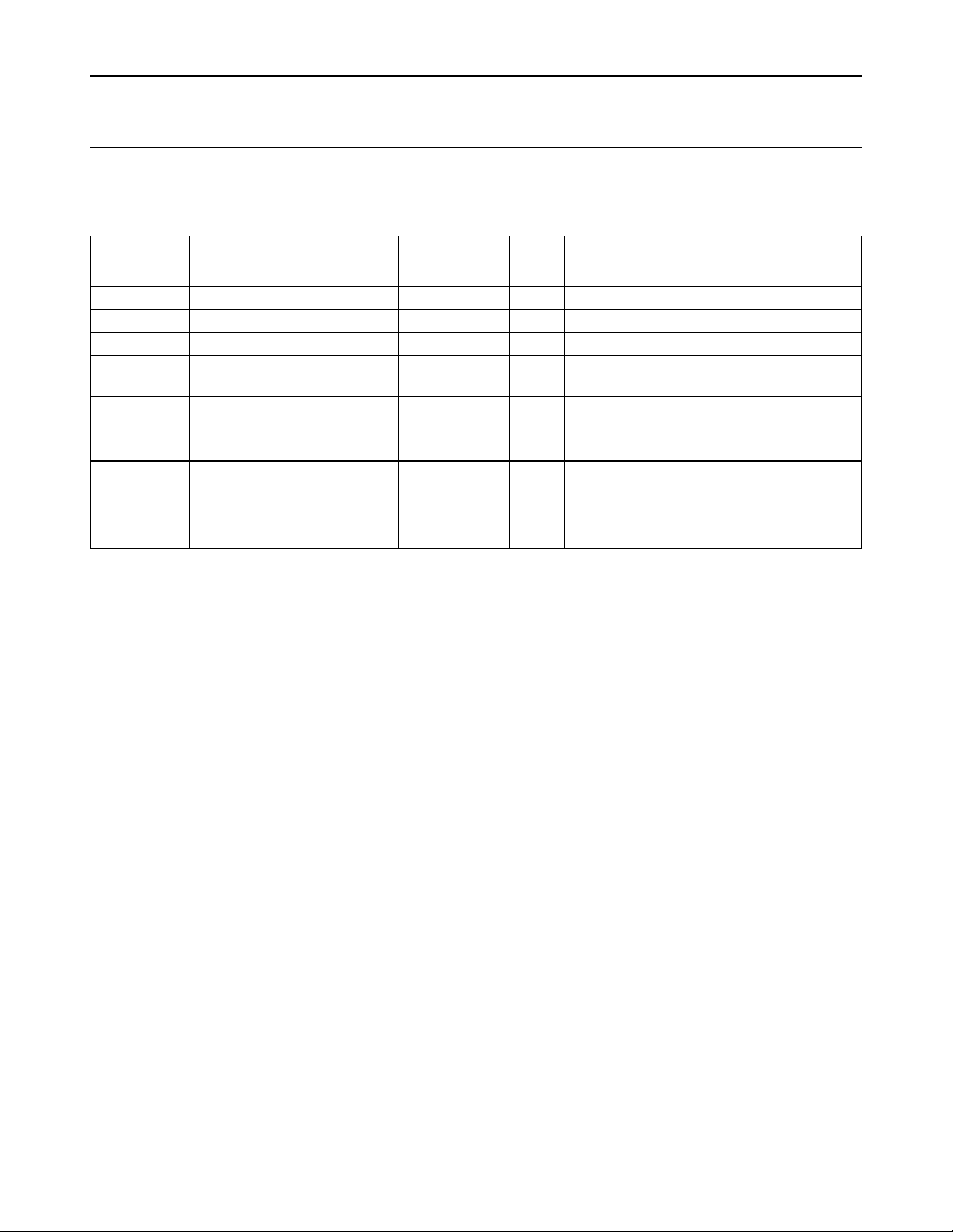
SYMBOL PARAMETER MIN. MAX. UNIT CONDITIONS
V
CC
V
O
I
IK
−I
OK
−I
O
DC supply voltage −0.5 +7 V
DC output voltage −0.5 +7 V
DC input diode current 20 mA for VI<−0.5 V or VI> VCC+ 0.5 V
DC output diode current 20 mA for VO<−0.5 V
DC output sink current 25 mA for − 0.5 V < V
O
±ICC;
±I
GND
T
stg
P
tot
DC VCC or GND current 50 mA
storage temperature range −65 +150 °C
power dissipation per package for temperature range; −40 to +125 °C
74HC/HCT
plastic DIL 750 mW above +70 °C: derate linearly with 12 mW/K
plastic mini-pack (SO) 500 mW above +70 °C: derate linearly with 8 mW/K
December 1990 4
Page 5
Philips Semiconductors Product specification
Quad 2-input NAND gate 74HC/HCT03
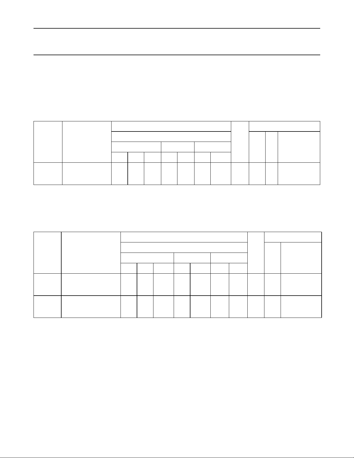
DC CHARACTERISTICS FOR 74HC
For the DC characteristics see
“74HC/HCT/HCU/HCMOS Logic Family Specifications”
not valid for open drain. They are replaced by IOZ as given below.
Output capability: standard (open drain), excepting V
OH
ICC category: SSI
Voltages are referenced to GND (ground = 0 V)
T
(°C) TEST CONDITIONS
amb
74HC
SYMBOL PARAMETER
+25 −40 to +85 −40 to +125
min. typ. max. min. max. min. max.
I
OZ
HIGH level output
leakage current 0.5 5.0 10.0 µA
Note
1. The maximum operating output voltage (V
O(max)
) is 6.0 V.
AC CHARACTERISTICS FOR 74HC
GND = 0 V; tr=tf= 6 ns; CL= 50 pF
(°C) TEST CONDITIONS
T
amb
74HC
SYMBOL PARAMETER
+25 −40 to +85 −40 to +125
min. typ. max. min. max. min. max.
t
PZL
t
PLZ
t
THL
/
propagation delay
nA, nB to nY
28
10
8
output transition time 19
7
6
95
19
16
75
15
13
120
24
20
95
19
16
, except that the VOH values are
UNIT V
VIOTHER
CC
(V)
2.0
to
V
IL
VO=V
or GND
6.0
UNIT
WAVEFORMS
V
CC
(V)
145
29
25
110
22
19
2.0
ns
4.5
6.0
ns 2.0
4.5
6.0
Fig.6
Fig.6
O(max)
(1)
December 1990 5
Page 6
Philips Semiconductors Product specification
Quad 2-input NAND gate 74HC/HCT03
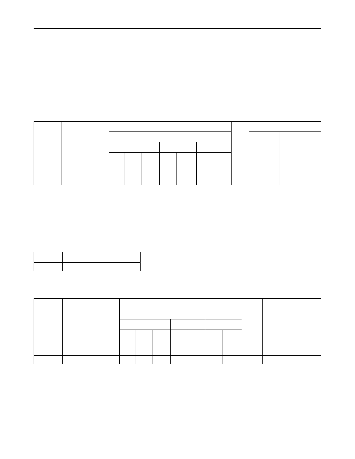
DC CHARACTERISTICS FOR 74HCT
For the DC characteristics see
“74HC/HCT/HCU/HCMOS Logic Family Specifications”
, except that the VOH values are
not valid for open drain. They are replaced by IOZ as given below.
Output capability: standard (open drain), excepting V
OH
ICC category: SSI
Voltages are referenced to GND (ground = 0 V)
T
amb
(°C)
TEST CONDITIONS
74HCT
SYMBOL PARAMETER
UNIT
V
(V)
CC
VIOTHER+25 −40 to +85 −40 to +125
min. typ. max. min. max. min. max.
I
OZ
HIGH level output
leakage current
0.5 5.0 10.0 µA
4.5
to
5.5
V
Note
1. The maximum operating output voltage (V
O(max)
) is 6.0 V.
Note to HCT types
The value of additional quiescent supply current (∆I
) for a unit load of 1 is given in the family specifications.
CC
To determine ∆ICC per input, multiply this value by the unit load coefficient shown in the table below.
IL
VO=V
or GND
O(max)
(1)
INPUT UNIT LOAD COEFFICIENT
nA, nB 1.0
AC CHARACTERISTICS FOR 74HCT
GND = 0 V; t
= 6 ns; CL= 50 pF
r=tf
SYMBOL PARAMETER
min. typ. max. min. max. min. max.
t
PZL
/ t
propagation delay
PLZ
nA, nB, to nY
t
THL
output transition time 7 15 19 22 ns 4.5 Fig.6
T
(°C) TEST CONDITIONS
amb
74HCT
+25 −40 to +85 −40 to +125
UNIT
WAVEFORMS
V
CC
(V)
12 24 30 36 ns 4.5 Fig.6
December 1990 6
Page 7
Philips Semiconductors Product specification
Quad 2-input NAND gate 74HC/HCT03
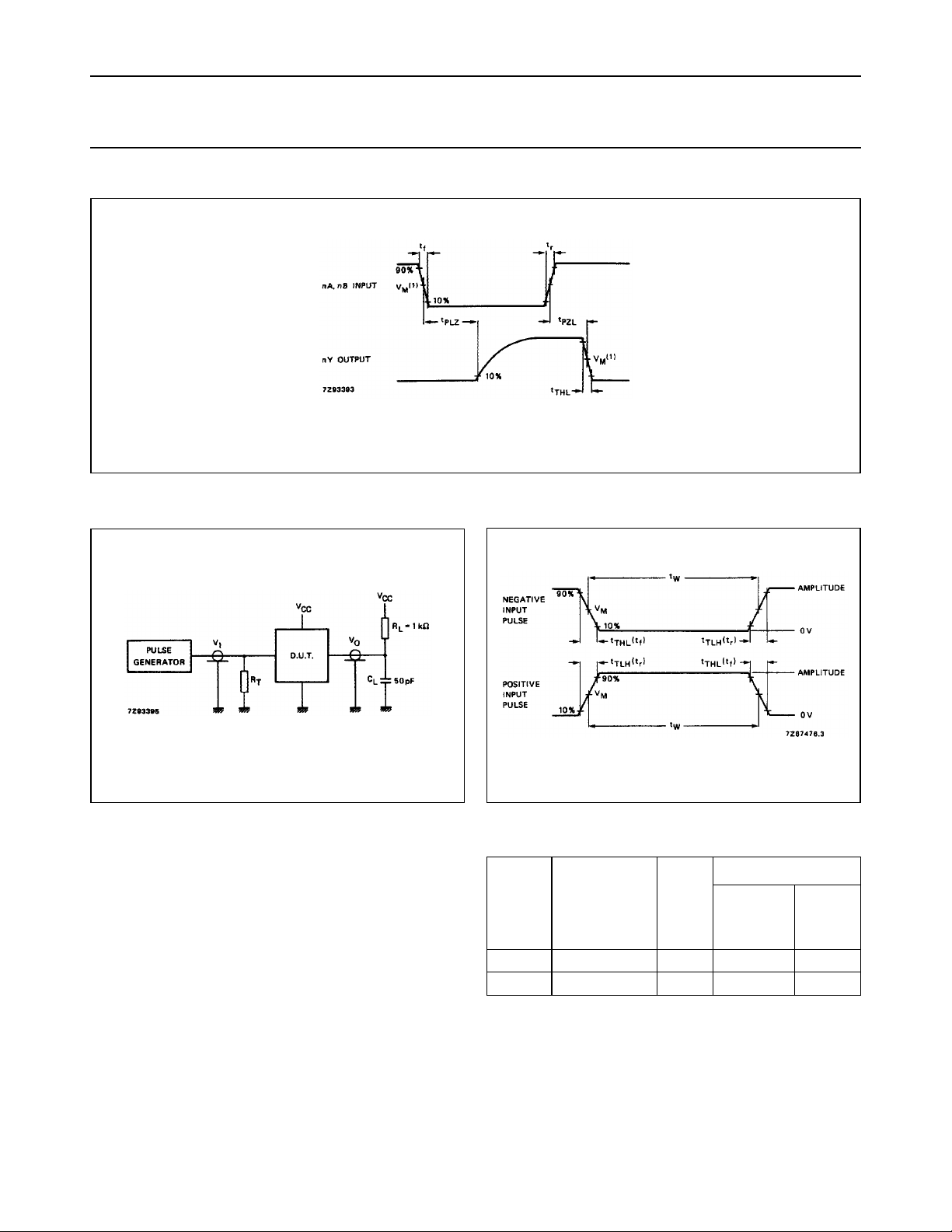
AC WAVEFORMS
HC: VM= 50%; VI= GND to V
HCT: VM= 1.3 V; VI= GND to 3 V.
CC
Fig.6 Waveforms showing the input (nA, nB) to output (nY) propagation delays and the output transition times.
TEST CIRCUIT AND WAVEFORMS
Fig.7 Test circuit (open drain)
Definitions for Figs. 7, 8:
Fig.8 Input pulse definitions.
C
= load capacitance including jig and probe
L
capacitance
(see AC CHARACTERISTICS for values).
= termination resistance should be equal to the
R
T
output impedance ZO of the pulse generator.
t
=tf= 6 ns; when measuring f
r
, there is no
max
constraint on tr, tf with 50% duty factor.
December 1990 7
tr;t
f
f
;
FAMILY AMPLITUDE V
M
max
PULSE
OTHER
WIDTH
74HC V
CC
50% < 2 ns 6 ns
74HCT 3.0 V 1.3 V < 2 ns 6 ns
Page 8
Philips Semiconductors Product specification
Quad 2-input NAND gate 74HC/HCT03
APPLICATION INFORMATION
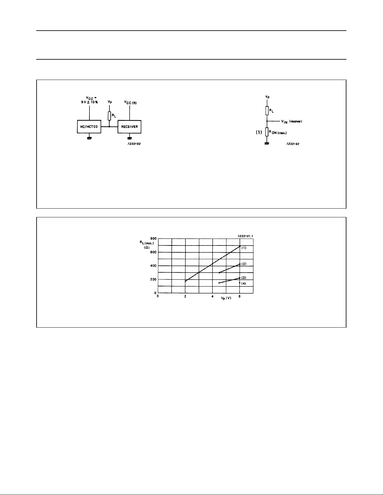
(1) R
(a)
= 0.26 V / 4 mA = 65 Ω (at 25 °C)
ON(max)
(b)
Fig.9 Pull-up configuration.
(1) VCC (R) = 2.0 V; VIL= 0.5 V.
(2) VCC (R) = 5.0 V; VIL= 0.8 V.
(3) VCC (R) = 4.5 V; VIL= 1.35 V.
(4) VCC (R) = 6.0 V; VIL= 1.8 V.
Fig.10 Minimum resistive load as a function of the pull-up voltage.
Notes to Figs 9 and 10
If VP− VCC (R) > 0.5 V a positive current will flow into the receiver (as described in the
“USER GUIDE
”; input/output
protection), this will not affect the receiver provided the current does not exceed 20 mA. At VCC< 4.5 V, R
guaranteed; R
can be estimated using Figs 33 and 34 in the
ON(max)
“USER GUIDE”
.
ON (max)
is not
Note to Application information
All values given are typical unless otherwise specified.
PACKAGE OUTLINES
See
“74HC/HCT/HCU/HCMOS Logic Package Outlines”
.
December 1990 8
 Loading...