

Page 1
INTEGRATED CIRCUITS
DATA SH EET
For a complete data sheet, please also download:
•The IC06 74HC/HCT/HCU/HCMOS Logic Family Specifications
•The IC06 74HC/HCT/HCU/HCMOS Logic Package Information
•The IC06 74HC/HCT/HCU/HCMOS Logic Package Outlines
74HC4049
Hex inverting high-to-low level
shifter
Product specification
File under Integrated Circuits, IC06
December 1990
Page 2
Philips Semiconductors Product specification
Hex inverting high-to-low level shifter 74HC4049
FEATURES
• Output capability: standard
• ICC category: SSI
This feature enables the inverting buffers to be used as
logic level translators, which will convert high level logic to
low level logic, while operating from a low voltage power
supply. For example 15 V logic (“4000B series”) can be
converted down to 2 V logic.
GENERAL DESCRIPTION
The 74HC4049 is a high-speed Si-gate CMOS device and
is pin compatible with the “4049” of the “4000B” series. It
is specified in compliance with JEDEC standard no. 7A.
The 74HC4049 provides six inverting buffers with a
modified input protection structure, which has no diode
connected to V
. Input voltages of up to 15 V may
CC
The actual input switch level remains related to the V
and is the same as mentioned in the family characteristics.
At the same time each part can be used as a simple
inverter without level translation.
APPLICATIONS
• Converting 15 V logic (“4000B” series) down to 2 V logic.
therefore be used.
QUICK REFERENCE DATA
GND = 0 V; T
=25°C; tr=tf= 6 ns
amb
SYMBOL PARAMETER CONDITIONS
t
PHL/tPLH
C
I
C
PD
propagation delay nA to nYC
input capacitance 3.5 pF
power dissipation capacitance per buffer note 1 14 pF
= 15 pF; VCC= 5 V 8 ns
L
CC
TYPICAL
UNIT
HC
Note
1. C
is used to determine the dynamic power dissipation (PD in µW):
PD
PD=CPD× V
2
× fi+ ∑ (CL× V
CC
2
× fo) where:
CC
fi= input frequency in MHz
fo= output frequency in MHz
CL= output load capacitance in pF
VCC= supply voltage in V
∑ (CL× V
2
× fo) = sum of outputs
CC
ORDERING INFORMATION
“74HC/HCT/HCU/HCMOS Logic Package Information”
See
.
December 1990 2
Page 3
Philips Semiconductors Product specification
Hex inverting high-to-low level shifter 74HC4049
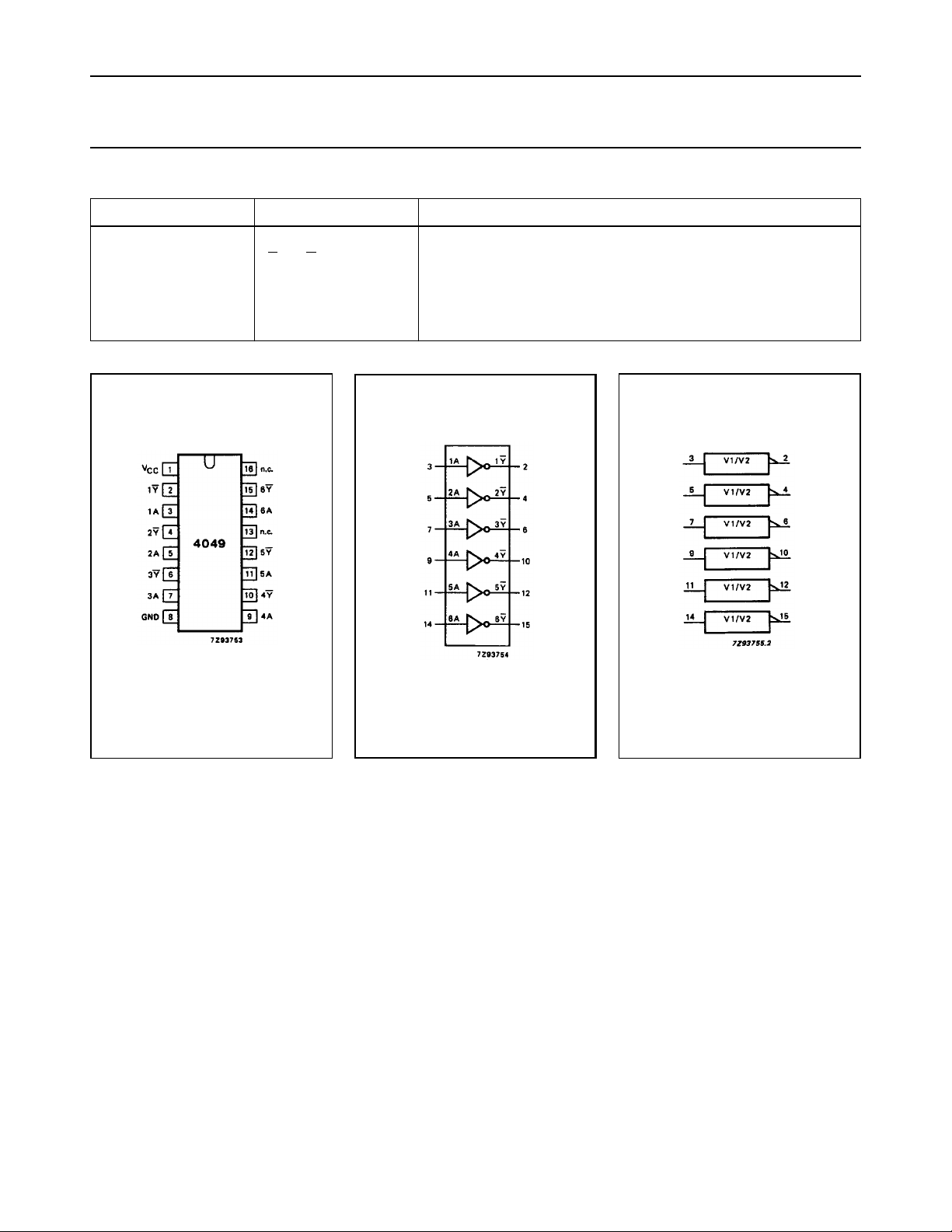
PIN DESCRIPTION
PIN NO. SYMBOL NAME AND FUNCTION
1V
2, 4, 6, 10, 12, 15 1
3, 5, 7, 9, 11, 14 1A to 6A data inputs
8 GND ground (0 V)
13, 16 n.c. not connected
CC
Y to 6Y data outputs
positive supply voltage
Fig.1 Pin configuration.
December 1990 3
Fig.2 Logic symbol. Fig.3 IEC logic symbol.
Page 4
Philips Semiconductors Product specification
Hex inverting high-to-low level shifter 74HC4049
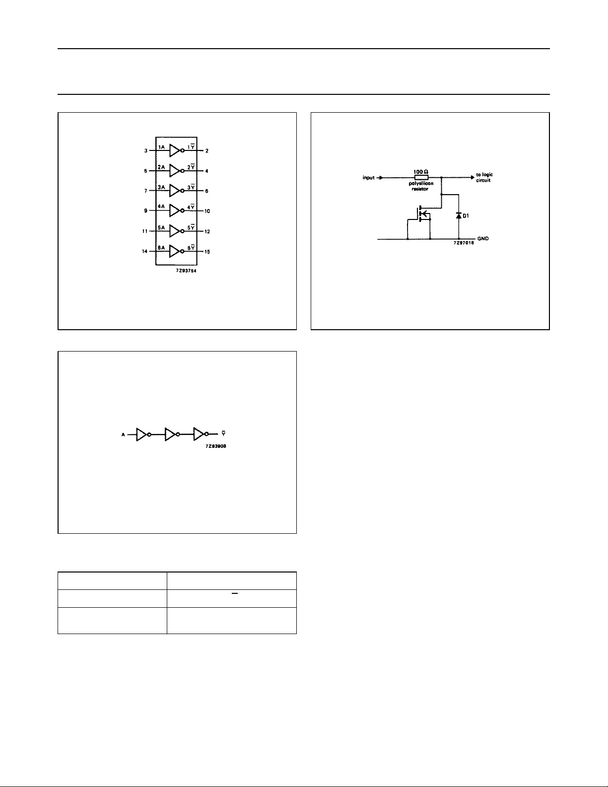
Fig.5 Input protection for HC4049. Single sided thick
Fig.4 Functional diagram.
oxide field effect metal gate transistor as input
protection.
Fig.6 Logic diagram (one level shifter).
FUNCTION TABLE
INPUT OUTPUT
nA n
L
H
Notes
1. H = HIGH voltage level
L = LOW voltage level
December 1990 4
Y
H
L
Page 5
Philips Semiconductors Product specification
Hex inverting high-to-low level shifter 74HC4049
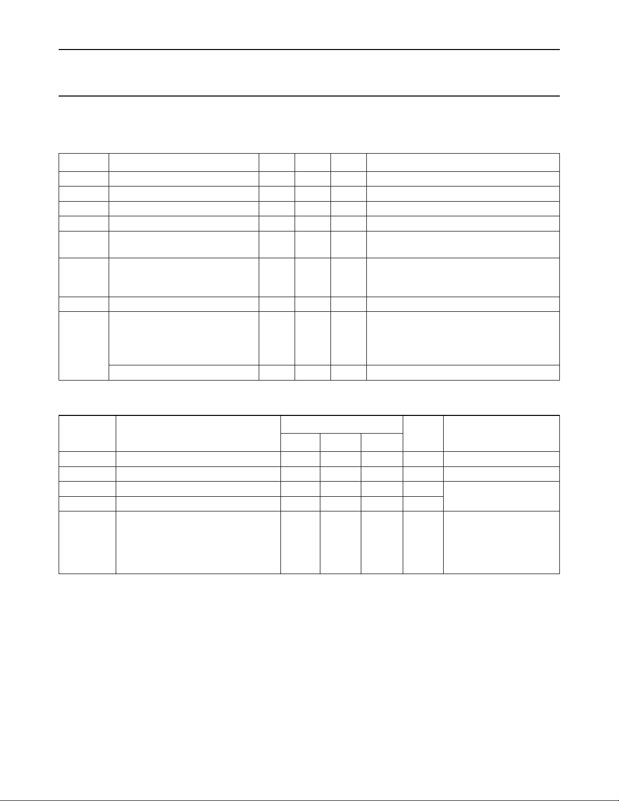
RATINGS
Limiting values in accordance with the Absolute Maximum System (IEC 134)
Voltages are referenced to GND (ground = 0 V)
SYMBOL PARAMETER MIN. MAX. UNIT CONDITIONS
V
CC
V
IK
−I
IK
±I
OK
±I
O
;
±I
CC
±I
GND
T
stg
P
tot
DC supply voltage −0.5 +7 V
DC input voltage range −0.5 +16 V
DC input diode current 20 mA for VI <−0.5 V
DC output diode current 20 mA for VO<−0.5 V or VO> VCC+0.5 V
DC output source or sink current
for −0.5 V < VO< VCC+0.5 V
- standard outputs 25 mA
DC VCCor GND current for types
with:
- standard outputs 50 mA
storage temperature range −65 +150 °C
power dissipation per package for temperature range: −40 to +125 °C
74HC
plastic DIL 750 mW above +70 °C: derate linearly with 12 mW/K
plastic mini-pack (SO) 400 mW above +70 °C: derate linearly with 8 mW/K
RECOMMENDED OPERATING CONDITIONS
SYMBOL PARAMETER
V
CC
V
I
T
amb
T
amb
t
, t
r
f
DC supply voltage 2.0 5.0 6.0 V
DC input voltage range GND − 15 V
operating ambient temperature range −40 +85 °C
operating ambient temperature range −40 +125 °C
input rise and fall times 6.0
74HC
min. typ. max.
1000
500
400
650
1000
UNIT CONDITIONS
see DC and AC
characteristics
VCC= 2.0 V; VIN= 2.0 V
VCC= 4.5 V; VIN= 4.5 V
ns
VCC= 6.0 V; VIN= 6.0 V
VCC= 6.0 V; VIN= 10.0 V
VCC= 6.0 V; VIN= 15.0 V
December 1990 5
Page 6
Philips Semiconductors Product specification
Hex inverting high-to-low level shifter 74HC4049
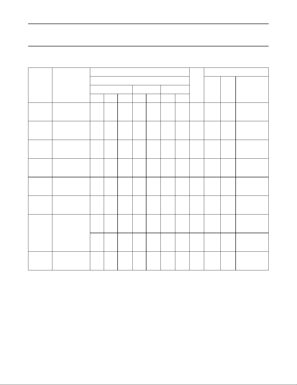
DC CHARACTERISTICS FOR 74HC
Voltages are referenced to GND (ground = 0 V)
SYMBOL PARAMETER
V
IH
HIGH level input
voltage
V
IL
LOW level input
voltage
V
OH
HIGH level
output voltage
all outputs
V
OH
HIGH level
output voltage
standard outputs
V
OL
LOW level
output voltage
all outputs
V
OL
LOW level
output voltage
standard outputs
± I
I
input leakage
current
I
CC
quiescent
supply current
(°C)
T
amb
74HC
min. typ. max. min. max. min. max.
1.5
3.15
4.2
1.9
4.4
5.9
3.98
5.48
1.3
2.4
3.1
0.7
1.8
2.3
2.0
4.5
6.0
0.5
1.35
1.8
0.1
0.1
0.1
0.26
0.26
1.5
3.15
4.2
1.9
4.4
5.9
3.84
5.34
0.5
1.35
1.8
0.1
0.1
0.1
0.33
0.33
1.5
3.15
4.2
0.5
1.35
1.8
1.9
4.4
5.9
3.7
5.2
0.1
0.1
0.1
0.4
0.4
0.1 1.0 1.0 µA 6.0 V
0.5 5.0 5.0 µA 2.0
2.0 20.0 40.0 µA 6.0 15 V
UNIT
V 2.0
4.5
6.0
V 2.0
4.5
6.0
V 2.0
4.5
6.0
V 4.5
6.0
V 2.0
4.5
6.0
V 4.5
6.0
to
6.0
TEST CONDITIONS
V
CC
(V)
V
or
V
V
or
V
V
or
V
V
or
V
V
IH
IL
IH
IL
IH
IL
IH
IL
CC
I
−IO=20µA
−IO=20µA
−IO=20µA
−IO= 4.0 mA
−IO= 5.2 mA
IO=20µA
IO=20µA
IO=20µA
IO= 4.0 mA
IO= 5.2 mA
or
GND
15 V
or
GND
OTHER+25 −40 to +85 −40 to +125
December 1990 6
Page 7
Philips Semiconductors Product specification
Hex inverting high-to-low level shifter 74HC4049
AC CHARACTERISTICS FOR 74HC
GND = 0 V; t
SYMBOL PARAMETER
/ t
t
PHL
PLH
/ t
t
THL
TLH
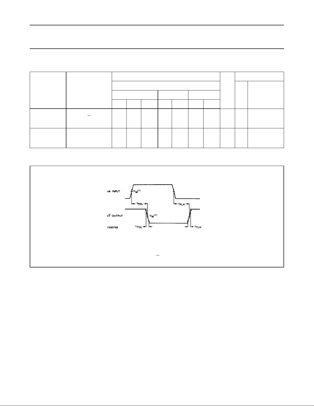
AC WAVEFORMS
= 6 ns; CL= 50 pF
r=tf
propagation delay
nA to nY
output transition
time
T
(°C)
amb
74HC
min. typ. max. min. max. min. max.
28
10
8
19
7
6
85
17
14
75
15
13
105
21
18
95
19
16
130
26
22
110
22
19
TEST CONDITIONS
UNIT
V
(V)
ns 2.0
4.5
6.0
ns 2.0
4.5
6.0
CC
WAVEFORMS+25 −40 to +85 −40 to +125
Fig.7
Fig.7
(1) HC: VM= 50%; VI= GND to VCC.
HCT: V
= 1.3 V; VI= GND to 3 V.
M
Fig.7 Waveforms showing the input (nA) to output (nY) propagation delays and the output transition times.
PACKAGE OUTLINES
“74HC/HCT/HCU/HCMOS Logic Package Outlines”
See
.
December 1990 7
 Loading...