

Page 1
Philips Semiconductors
Product specification
74F835
8-bit shift register with 2:1 mux-in,
latched “B” inputs, and serial out
1
1990 Jan 08 853–0615 99490
FEATURES
•Specifically designed for Video applications
•Combines the 74F373, two 74F157s, and the 74F166 functions in
one package
•Interleaved loading with 2:1 mux
•Dual 8-bit parallel inputs
•Transparent latch on all “B” inputs
•Guaranteed serial shift frequency to 100MHz
•Expandable to 16-bits or more with serial input
DESCRIPTION
The 74F835 is a high speed 8-bit parallel/serial-in, serial-out shift
register whose parallel inputs have been connected to an internal
octal two-to-one multiplexer with all the “B” inputs connected to an
octal latch.
This 24-pin part is specifically designed for video bit shifting, where
interleaved loading is desired and parts count is critical. It is useful in
any design where a 2:1 mux input with a transparent latch is
needed.
TYPE
TYPICAL f
MAX
TYPICAL
SUPPLY CURRENT
(TOTAL)
74F835 150MHz 45mA
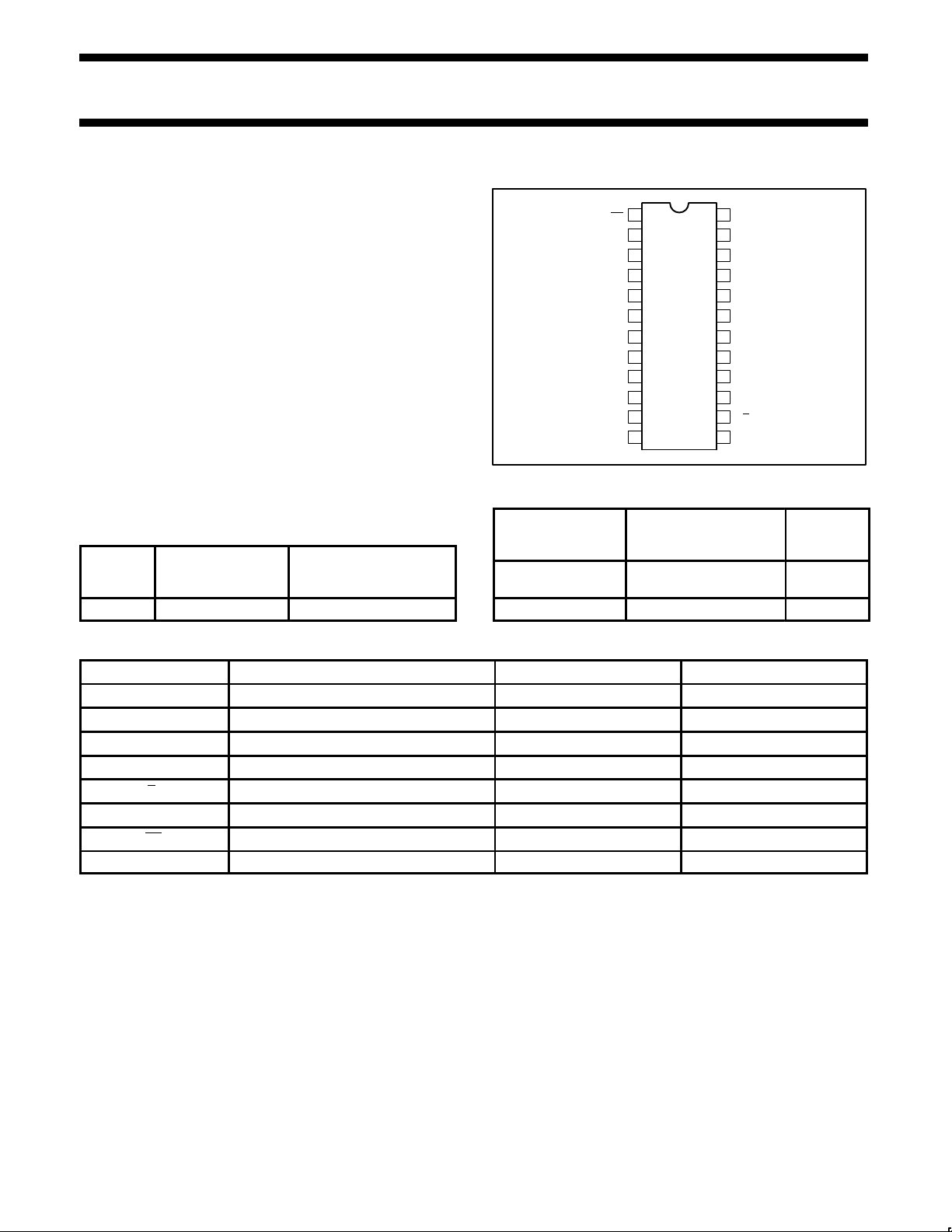
PIN CONFIGURATION
1
2
3
4
5
6
7
8
9
10
11
12 13
14
15
16
17
18
19
20
21
22
23
24
PE
CP
D4A
D4B
D5A
D5B
D6A
D6B
D7A
D7B
Q7
V
CC
D3B
D3A
D2B
D2A
D1B
D1A
D0A
D0B
DS
SA
/B
LE
GND
SF01355
ORDERING INFORMATION
DESCRIPTION
COMMERCIAL RANGE
V
CC
= 5V ±10%,
T
amb
= 0°C to +70°C
PACKAGE
DRAWING
NUMBER
24-pin plastic
Slim DIP (300 mil)
N74F835N SOT222-1
24-pin plastic SOL N74F835D SOT137-1
INPUT AND OUTPUT LOADING AND FAN-OUT TABLE
PINS DESCRIPTION 74F (U.L.) HIGH/LOW LOAD VALUE HIGH/LOW
D0A – D7A Parallel data inputs 1.0/1.0 20µA/0.6mA
D0B – D7B Latched Parallel data inputs 1.0/1.0 20µA/0.6mA
DS Serial data input 1.0/1.0 20µA/0.6mA
CP Shift Register Clock input (active rising edge) 1.0/1.0 20µA/0.6mA
SA/B Mux Select 1.0/1.0 20µA/0.6mA
LE Latch Enable input (for B inputs) 1.0/1.0 20µA/0.6mA
PE Parallel Enable input 1.0/1.0 20µA/0.6mA
Q7 Output 50/33 1.0mA/20mA
NOTE: One (1.0) FAST unit load is defined as: 20µA in the High state and 0.6mA in the Low state.
Page 2

Philips Semiconductors Product specification
74F835
8-bit shift register with 2:1 mux-in,
latched “B” inputs, and serial out
1990 Jan 08
2
LOGIC SYMBOL
2
1
13
14
CP
PE
LE
SA
/B
15 16 17 18 19 20 21 22 23 3 4 5 6 7 8 9 10
11
Q7
DS
D0A
D0B
D1A
D1B
VCC = PIN 24
GND = PIN 12
SF01356
D2A
D2B
D3A
D3B
D4A
D4B
D5A
D5B
D6A
D6B
D7A
D7B
IEC/IEEE SYMBOL
SF01357
2
C1
SRG 8
MUX
1
M4
13
EN3
14
G2
15
1,4
16
1, 2
, 3, 4
17
1, 2, 3, 4
18
19
20
21
22
23
3
4
5
6
7
8
9
10
11
TYPICAL TIMING DIAGRAM
SET B
UNLOAD
B LATCH
SHIFT BSHIFT A
LOAD A
LOAD B LATCH
PE
CP
LE
SA
/B
D0A
D7A
D0B
D7B
Q7
q7A q6A q1A q0A q7B q6B q5B q0B
SF01359
Page 3
Philips Semiconductors Product specification
74F835
8-bit shift register with 2:1 mux-in,
latched “B” inputs, and serial out
1990 Jan 08
3
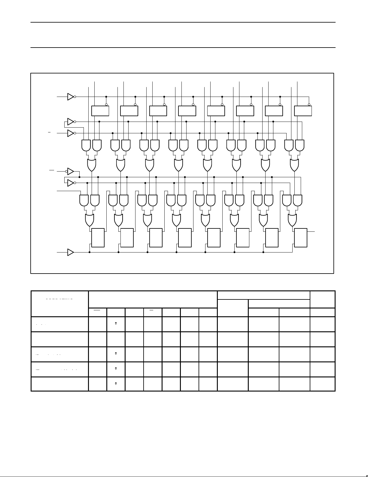
LOGIC DIAGRAM
VCC = PIN 24
GND = PIN 12
D Q
CP
D Q
CP
D Q
CP
D Q
CP
D Q
CP
D Q
CP
D Q
CP
D Q
CP
11
Q7
D E
Q
D E
Q
D E
Q
D E
Q
D E
Q
D E
Q
D E
Q
D E
Q
16
17
18
19
20
21
22
23
3
4
5
6
7
8
9
10
D0A
D0B
D1A
D1B
D2A
D2B
D3A
D3B
D4A
D4B
D5A
D5B
D6A
D6B
D7A
D7B
LE
13
14
1
15
2
SA
/B
PE
DS
CP
SF01358
FUNCTION TABLE
INTERNAL
OPERATING
INPUTS
B
SERIAL REGISTER
OUTPUT
MODE
PE CP LE SA/B DnA DnB DS
B
LATCH
Q0 Q1–6 Q7
h X X X H H H
Parallel load
A data
L↑X
L
l X X X L L L
X h X H X X X
Latch B data
XXL
X
X l X L X X X
X X X h H H H
Parallel load B data
(from Latch)
L↑L
H
X X X l L L L
X h X h H H H
Parallel load B data
(Transparent Mode)
L↑H
H
X l X l L L L
X X h X H qn–1 q6
Serial Shift
H↑X
X
X X l X L qn–1 q6
H = High voltage level
L = Low voltage level
h = High voltage level one setup time prior to the Low-to-High clock transition
l = Low voltage level one setup time prior to the Low-to-High clock transition
X = Don’t care
qn = Lower case letters indicate the state of the referenced flop cell one cycle prior to the Low-to-High clock transition
↑ = Low-to-High clock transition
Parallel load
Parallel load B data
Parallel load B data
Page 4
Philips Semiconductors Product specification
74F835
8-bit shift register with 2:1 mux-in,
latched “B” inputs, and serial out
1990 Jan 08
4
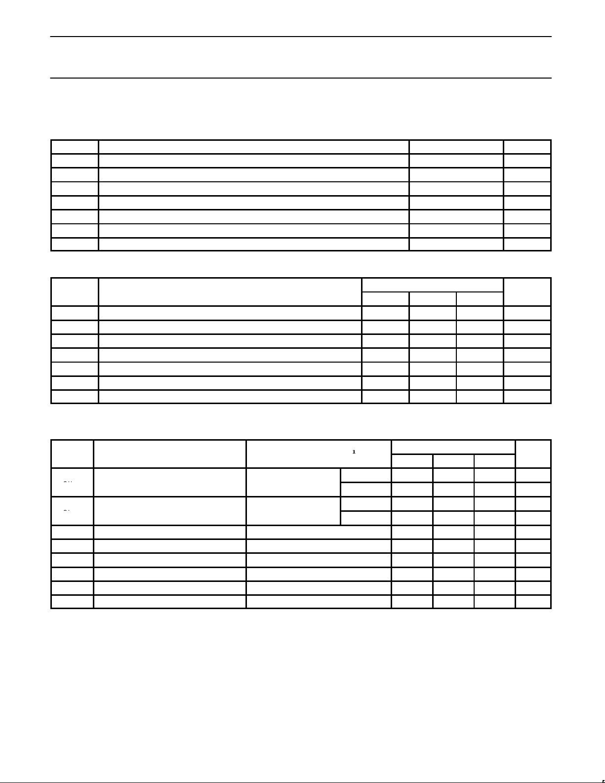
ABSOLUTE MAXIMUM RATINGS
(Operation beyond the limits set forth in this table may impair the useful life of the device.
Unless otherwise noted these limits are over the operating free-air temperature range.)
SYMBOL
PARAMETER RATING UNIT
V
CC
Supply voltage –0.5 to +7.0 V
V
IN
Input voltage –0.5 to +7.0 V
I
IN
Input current –30 to +5 mA
V
OUT
Voltage applied to output in High output state –0.5 to V
CC
V
I
OUT
Current applied to output in Low output state 40 mA
T
amb
Operating free-air temperature range 0 to +70 °C
T
stg
Storage temperature range –65 to +150 °C
RECOMMENDED OPERATING CONDITIONS
LIMITS
SYMBOL
PARAMETER
MIN NOM MAX
UNIT
V
CC
Supply voltage 4.5 5.0 5.5 V
V
IH
High-level input voltage 2.0 V
V
IL
Low-level input voltage 0.8 V
I
IK
Input clamp current –18 mA
I
OH
High-level output current –1 mA
I
OL
Low-level output current 20 mA
T
amb
Operating free-air temperature range 0 +70 °C
DC ELECTRICAL CHARACTERISTICS
(Over recommended operating free-air temperature range unless otherwise noted.)
LIMITS
SYMBOL
PARAMETER
TEST CONDITIONS
1
MIN TYP
2
MAX
UNIT
CC
= MIN, VIL = MAX
±10% V
CC
2.5 V
VOHHigh-level output voltage
VCC = MIN, VIL = MAX
V
IH
= MIN, IOH = MAX
±5% V
CC
2.7 3.4 V
CC
= MIN, VIL = MAX
±10% V
CC
0.30 0.50 V
VOLLow-level output voltage
VCC = MIN, VIL = MAX
VIH = MIN, IOHL= MAX
±5% V
CC
0.30 0.50 V
V
IK
Input clamp voltage VCC = MIN, II = I
IK
–0.73 –1.2 V
I
I
Input current at maximum input voltage VCC = MAX, VI = 7.0V 100 µA
I
IH
High-level input current VCC = MAX, VI = 2.7V 20 µA
I
IL
Low-level input current VCC = MAX, VI = 0.5V –0.6 mA
I
OS
Short circuit output current
3
VCC = MAX –60 –150 mA
I
CC
Supply current (total) VCC = MAX 45 65 mA
NOTES:
1. For conditions shown as MIN or MAX, use the appropriate value specified under recommended operating conditions for the applicable type.
2. All typical values are at V
CC
= 5V. T
amb
= 25°C.
3. Not more than one output should be shorted at a time. For testing I
OS
, the use of high-speed test apparatus and/or sample-and-hold
techniques are preferable in order to minimize internal heating and more accurately reflect operational values. Otherwise, prolonged shorting
of a High output may raise the chip temperature well above normal and thereby cause invalid readings in other tests. In any sequence of
parameter tests, I
OS
tests should be performed last.
V
V
Page 5
Philips Semiconductors Product specification
74F835
8-bit shift register with 2:1 mux-in,
latched “B” inputs, and serial out
1990 Jan 08
5
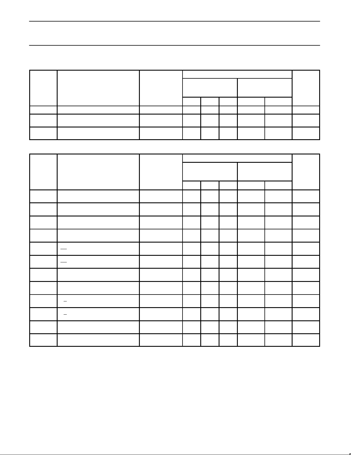
AC ELECTRICAL CHARACTERISTICS
LIMITS
SYMBOL
PARAMETER
TEST
CONDITION
T
amb
= +25°C
V
CC
= +5.0V
C
L
= 50pF, RL = 500Ω
T
amb
= 0°C to +70°C
V
CC
= +5.0V ± 10%
C
L
= 50pF, RL = 500Ω
UNIT
MIN TYP MAX MIN MAX
f
MAX
Maximum clock frequency Waveform 1 130 150 100 MHz
t
PLH
t
PHL
Propagation delay
CP to Q7 (Load)
Waveform 1
5.0
5.0
7.0
7.0
9.5
9.5
5.0
5.0
10.0
10.0
ns
t
PLH
t
PHL
Propagation delay
CP to Q7 (Shift)
Waveform 1
5.0
5.0
7.0
7.0
9.5
9.5
5.0
5.0
10.0
10.0
ns
AC SETUP REQUIREMENTS
LIMITS
SYMBOL
PARAMETER
TEST
CONDITION
T
amb
= +25°C
V
CC
= +5.0V
CL = 50pF, RL = 500Ω
T
amb
= 0°C to +70°C
V
CC
= +5.0V ± 10%
CL = 50pF, RL = 500Ω
UNIT
MIN TYP MAX MIN MAX
ts(H)
t
s
(L)
Setup time
DnA or DnB to CP
Waveform 2
3.5
3.5
3.5
3.5
ns
th(H)
th(L)
Hold time
DnA or DnB to CP
Waveform 2
1.0
1.0
1.5
1.5
ns
ts(H)
t
s
(L)
Setup time
DS to CP
Waveform 2
1.0
1.0
1.5
1.5
ns
th(H)
t
h
(L)
Hold time
DS to CP
Waveform 2
2.0
2.0
2.5
2.5
ns
ts(H)
t
s
(L)
Setup time
PE
to CP
Waveform 2
3.5
3.5
4.0
4.0
ns
th(H)
th(L)
Hold time
PE to CP
Waveform 2
0.0
0.0
0.0
0.0
ns
ts(H)
t
s
(L)
Setup time
DnB to LE
Waveform 2
0.0
0.0
0.0
0.0
ns
th(H)
t
h
(L)
Hold time
DnB to LE
Waveform 2
3.0
3.0
4.0
4.0
ns
ts(H)
t
s
(L)
Setup time
SA
/B to CP
Waveform 2
4.5
4.5
5.0
5.0
ns
th(H)
t
h
(L)
Hold time
SA
/B to CP
Waveform 2
0.0
0.0
0.0
0.0
ns
tw(H)
t
w
(L)
clock pulse width,
High or Low
Waveform 1
4.5
4.5
5.5
5.0
ns
tw(H)
Latch Enable pulse width,
High
Waveform 1 4.5 5.0 ns
Page 6
Philips Semiconductors Product specification
74F835
8-bit shift register with 2:1 mux-in,
latched “B” inputs, and serial out
1990 Jan 08
6
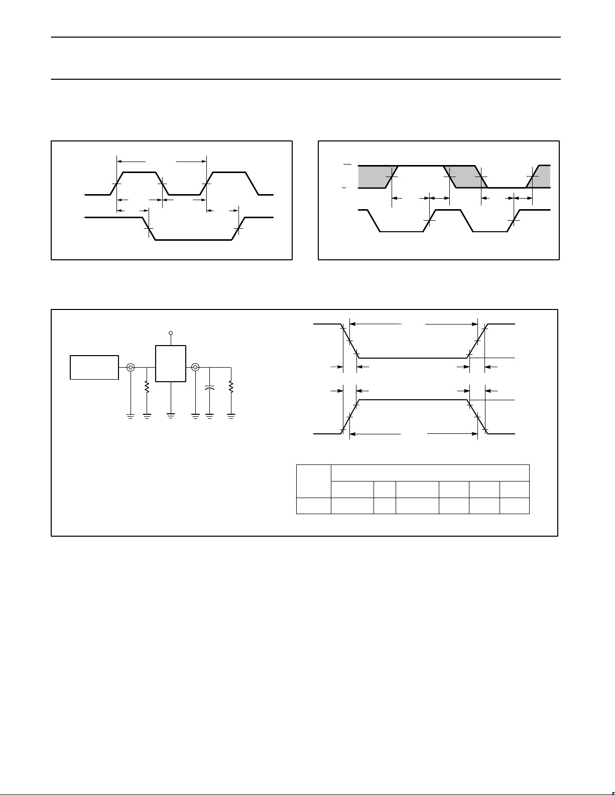
AC WAVEFORMS
For all waveforms, VM = 1.5V.
The shaded areas indicate when the input is permitted to change for predictable output performance.
tW(H)
CP
Q7
V
M
V
M
V
M
V
M
V
M
1/f
MAX
tW(L)
t
PHL
t
PLH
SF00287
Waveform 1. Propagation Delay, Clock Input to Output,
Clock Pulse Width, and Maximum Clock Frequency
V
M
V
M
th(H)
ts(H)
DS, PE
CP, LE
SF01360
DnA, DnB
SA/B
V
M
V
M
V
M
th(L)
ts(L)
V
M
Waveform 2. Data and Select Setup and Hold Times
TEST CIRCUIT AND WAVEFORMS
t
w
90%
V
M
10%
90%
V
M
10%
90%
V
M
10%
90%
V
M
10%
NEGATIVE
PULSE
POSITIVE
PULSE
t
w
AMP (V)
0V
0V
t
THL (tf
)
INPUT PULSE REQUIREMENTS
rep. rate
t
w
t
TLHtTHL
1MHz 500ns
2.5ns 2.5ns
Input Pulse Definition
V
CC
family
74F
D.U.T.
PULSE
GENERATOR
R
L
C
L
R
T
V
IN
V
OUT
Test Circuit for Totem-Pole Outputs
DEFINITIONS:
R
L
= Load resistor;
see AC ELECTRICAL CHARACTERISTICS for value.
CL= Load capacitance includes jig and probe capacitance;
see AC ELECTRICAL CHARACTERISTICS for value.
RT= Termination resistance should be equal to Z
OUT
of
pulse generators.
t
THL (tf
)
t
TLH (tr
)
t
TLH (tr
)
AMP (V)
amplitude
3.0V
1.5V
V
M
SF00006
 Loading...