

Page 1

Philips Semiconductors FAST Products Product specification
FAST 74F807
Octal shift/count registered transceiver
with adder and parity (3–State)
1
June 18, 1991 853–1421 02931
FEATURES
• High speed parallel registers with
positive edge–triggered D–type
flip–flops
• High speed full adder
• 8–bit parity generator
• High impedance PNP inputs for light
bus loading
• Center V
CC
and GND pins and controlled output buffers minimize
ground–bounce problems
• 3–State glitch–free power–up and
power–down
• Broadside pinout
DESCRIPTION
The 74F807 is a registered transceiver
that also has the capability to perform
count, shift, and add functions. It is also
has the capability to generate a parity
bit output. All of this is done within a
28–pin package.
The MR
input is an overriding
asynchronous reset which forces the
STATOUT output low as well as the A
and B busses.
The A and B busses have separate OE
inputs (OEA, OEB]. These inputs have
no bearing on the internal functioning of
this device only on the output states.
Both OE
pins are enabled low.
All operating modes, other than clear,
3–State, and the two hold modes require the rising edge of the clock. All
setup and hold times must be observed
for proper functioning.
Data on the internal register can be
switched on either the A or B ports for
output.
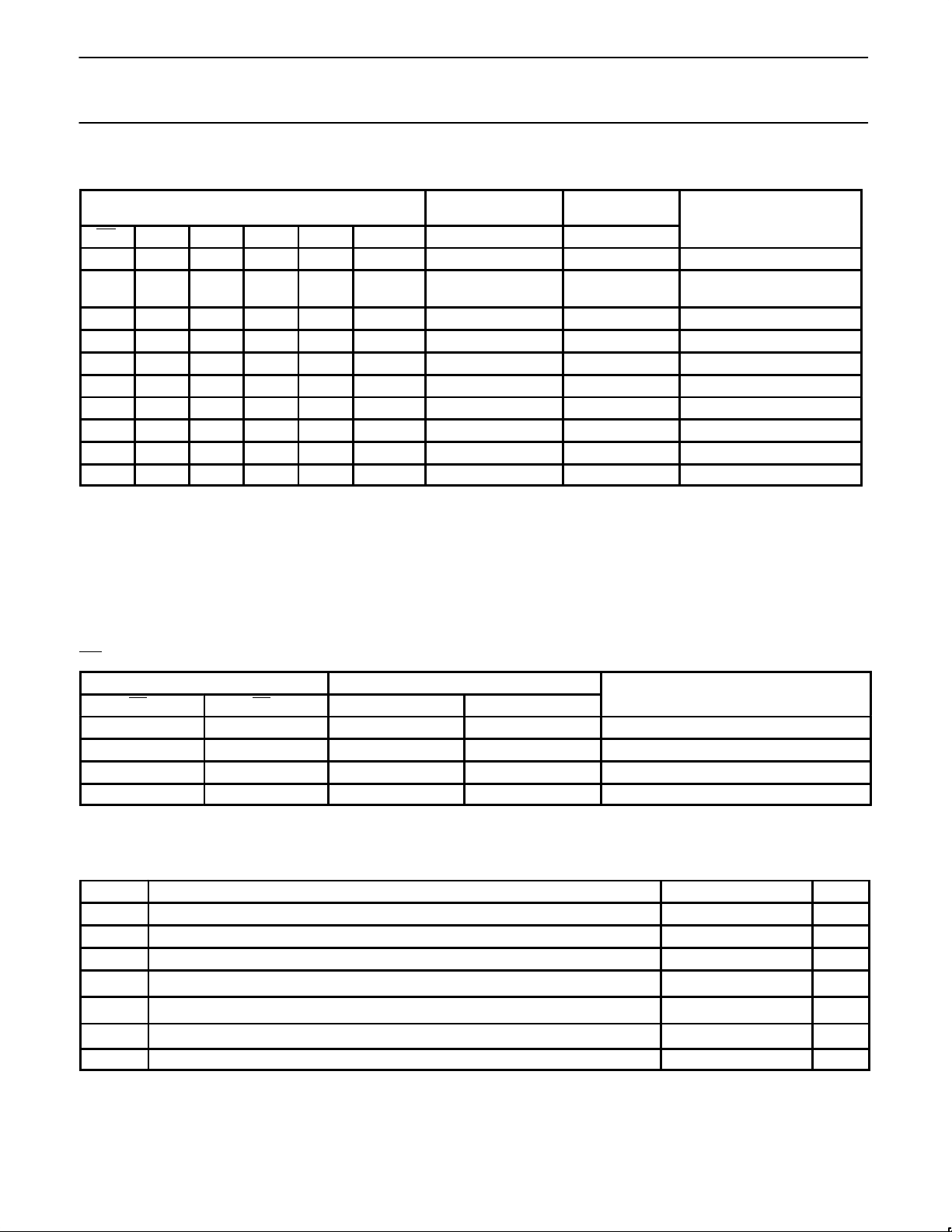
Depeding on the state of the select inputs (S0, S1, S2), and carry in/ serial in/
clock enable (CI/SI/CE), the 74F807 has
nine distinct operating modes:
1. Add mode w/carry in – the CI/SI/CE
input is used as a carry in signal and the
STATOUT output is the carry out signal.
(In add mode the COUT is NOT
registered. This means the carry output
signal appears at the STATOUT output
one clock prior to the related data.). In
this mode, the CI/SI/CE input is added
to the register contents and to the
inputs. (The adder uses only the An
inputs, not the Bn inputs.)
2. Add mode wo/carry in –– same as above
except the CI/SI/CE input is not included in
the addition.
3. Count w/count enable (count) –– the CI/SI/
CE input is now used as the count enable
input and the STATOUT output is terminal
count. In this mode the CI/SI/CE input must
be high to enable the count function. The
register contents are incremented by one.
4. Count w/count enable (hold) –– same as
above except no incrementing occurs.
5. Count wo/count enable –– same as number 3 except the CI/SI/CE input has no control over counting or holding.
6. Shift –– The CI/SI/CE input now becomes
the serial input and the STATOUT output
becomes the serial output. In this mode the
CI/SI/CE input is shifted into the Q0 register,
Q0 into the Q1 register etc. The Q7 register
is shifted into the STATOUT.
7. Load A inputs –– The CI/SI/CE input has
no bearing in either of the load modes. The
STATOUT output becomes the parity out.
The parity out is high for an odd number of
registered bits high, and low for even number
of registered bits high (even parity). In this
mode the An inputs are loaded into the
internal register and output to the B bus. If
OEA
= low the internal register would wrap
around and be loaded again.
8. Load B inputs –– same as number 7
except the A and B busses are switched.
9. Hold –– Again the CI/SI/CE input is not
used; the STATOUT output is still the parity
out. In this mode either the A bus, B bus or
both can be held with the registered data. No
other operation is performed.
TYPE
TYPICAL f
max
TYPICAL SUPPLY CURRENT (TOTAL)
74F807 115MHz 155mA
ORDERING INFORMATION
ORDER CODE
DESCRIPTION COMMERCIAL RANGE
V
CC
= 5V ±10%, T
amb
= 0°C to +70°C
28–pin plastic DIP (300 mils) N74F807N
28–pin SOL
1
N74F807D
28–pin PLCC N74F807A
Note to ordering information
1.Thermal mounting techiques are recommended. See SMD Process Applications (page 17) for a discussion of thermal consideration for surface
mounted devices.
Page 2

Philips Semiconductors FAST Products Product specification
FAST 74F807
Octal shift/count registered transceiver
with adder and parity (3–State)
June 18, 1991
2
INPUT AND OUTPUT LOADING AND FAN OUT TABLE
PINS DESCRIPTION
74F (U.L.) HIGH/LOW LOAD VALUE HIGH/LOW
An, Bn Data I/O inputs 3.5/0.166
70µA/70µA
OEA, OEB A output enable inputs 1.0/0.033
20µA/20µA
CI/SI/CE Carry in/serial in/clock enable input 1.0/0.033
20µA/20µA
CP Clock input 1.0/0.033
20µA/20µA
MR Master reset input (active low) 1.0/0.033
20µA/20µA
Sn Select inputs 1.0/0.033
20µA/20µA
STATOUT Status out output 150/40 3mA/24mA
An, Bn Data I/O outputs 150/40 3mA/24mA
Note to input and output loading and fan out table
1. One (1.0) FAST unit load is defined as: 20
µA in the high state and 0.6mA in the low state.
PIN CONFIGURATION PIN CONFIGURATION PLCC
1
2
3
4
5
6
7
8
9
10 19
20
21
22
23
24
25
26
27
28
OEA
OEB
A0
A1
A2
A3
GND
GND
A4
A5
A6
A7
CI/SI/CE
CP
4 3 2 1 28 27
25
24
23
22
21
20
11
10
9
8
7
6
18
16 17151413
26
19
12
5
PLCC
A2
A3
GND
GND
A4
A5
A6
11
12
13
14 15
16
17
18
V
CC
OEAA0A1 MR
STAT
OUT
B0
B7
S2CPCI/
SI/
CE
A7
MR
STATOUT
B0
B1
B2
B3
B4
B5
B6
B7
S0
S1
S2
OEB
S1 S0
B1
B2
B3
V
CC
B4
B5
B6
LOGIC SYMBOL IEC/IEEE SYMBOL
2
1
EN3
3
4
5
8
9
10
11
13
13
17
16
15
14
28
1
2
26
25
24
23
21
20
19
18
R
EN1
EN2
0
3
M
1
15
27
STATUS
OUT
OEA
OEB
CI/SI/CE
MR
VCC = Pin 22
GND = Pin 7, 8
3 4 5 6 9 10 11 12
26 25 24 23 22 20 19 18
1
2
13
28
STATOUT 27
B0 B1 B2 B3 B4 B5 B6 B7
A0 A1 A2 A3 A4 A5 A6 A7
Page 3

Philips Semiconductors FAST Products Product specification
FAST 74F807
Octal shift/count registered transceiver
with adder and parity (3–State)
June 18, 1991
3
LOGIC DIAGRAM
Qn
SHIFTOUT
OEA
OEB
CP
MR
CI/SI/CE
S0
V
CC =
Pin 22,
GND = Pin 7, 8
1
2
14
28
13
17
LE
An
QIN
CIN
ADDER
SUMn
COUT
8
8
8
8
LE
Dn
DATA
REGISTERS
CP
TC
R
TCIN
TC
REGISTER
CP
QIN P0
PARITY
QIN
An
Bn
SUMn
CI/SI/CE
2 – 7,
9 – 12
26 –23,
21 – 18
27
8
8
8
8
RCOUT
R
E
G
I
S
T
E
R
C
O
N
T
R
O
L
STATOUT
A0 – A7
B0 – B7
16
15
S1
S2
HOLD
LOAD A
LOAD B
CNTE
CNTNE
CNT
SHIFT
ADD
Page 4
Philips Semiconductors FAST Products Product specification
FAST 74F807
Octal shift/count registered transceiver
with adder and parity (3–State)
June 18, 1991
4
FUNCTION TABLE
INPUTS
INTERNAL
REGISTER
OUTPUT
OPERATING MODE
MR CP SO S1 S2 CI/SI/CE Qn STATOUT
L X X X X X L L Clear
H ↑ L L L CI/SI/CE
CI/SI/CE + an0 + qn0
COUT Add mode w/carry in
H ↑ L L H X an0 + qn0 COUT Add mode wo/carry in
H ↑ L H L H qn0 + 1 TC (1) Count w/count enable (count)
H X L H H L qn0 TC (1) Count w/count enable (hold)
H ↑ L H H X qn0 + 1 TC (1) Count wo/count enable
H ↑ H L L CI/SI/CE (3) Q7 Shift
H ↑ H L H X An0 parity (2) Load A ports
H ↑ H H L X Bn0 parity (2) Load B ports
H X H H H X Qn0 parity (2) Hold
Notes to function table
1. H = High–voltage level
2. L = Low–voltage level
3. a, b, q = Lower case indicate the state of the referenced output prior to the low–to–high clock transition
4. X = Don’t care
5. Z = High impedance ”off)” state
6. ↑ = Low–to–high clock transition.
7. (1) = Terminal count is high when the output is a terminal count (HHHHHHHH).
8. (2) = Parity is high for odd number of internal register bits high, low for even number of internal register bits high.
9. (3) = CI/SI/CE → Q0 → Q1, etc.
OE FUNCTION TABLE
INPUTS OUTPUTS MODE
OEa OEb An Bn
L L active output active output Enable A and B outputs
L H active output input Enable A outputs, B inputs
H L input active output A inputs, enable B outputs
H H input input A and B are inputs
NOTE: The outputs, whether An or Bn, are equal to the INTERNAL REGISTER Qn.
ABSOLUTE MAXIMUM RATINGS (Operation beyond the limits set forth in this table may impair the useful life of the device. Unless
otherwise noted, these limits are over the operating free–air temperature range.)
SYMBOL
PARAMETER RATING UNIT
–0.5 to +7.0 V
V
IN
Input voltage –0.5 to +7.0 V
I
IN
–30 to +5 mA
–0.5 to V
CC
V
Current applied to output in low output state 48 mA
T
amb
0 to +70
°C
Tstg
–65 to +150
°C
NOTE: When outputs are disabled the internal registers (Qn) operate as usual.
V
CC
V
OUT
I
OUT
Supply voltage
Input current
Voltage applied to output in high output state
Operating free air temperature range
Storage temperature range
Page 5
Philips Semiconductors FAST Products Product specification
FAST 74F807
Octal shift/count registered transceiver
with adder and parity (3–State)
June 18, 1991
5
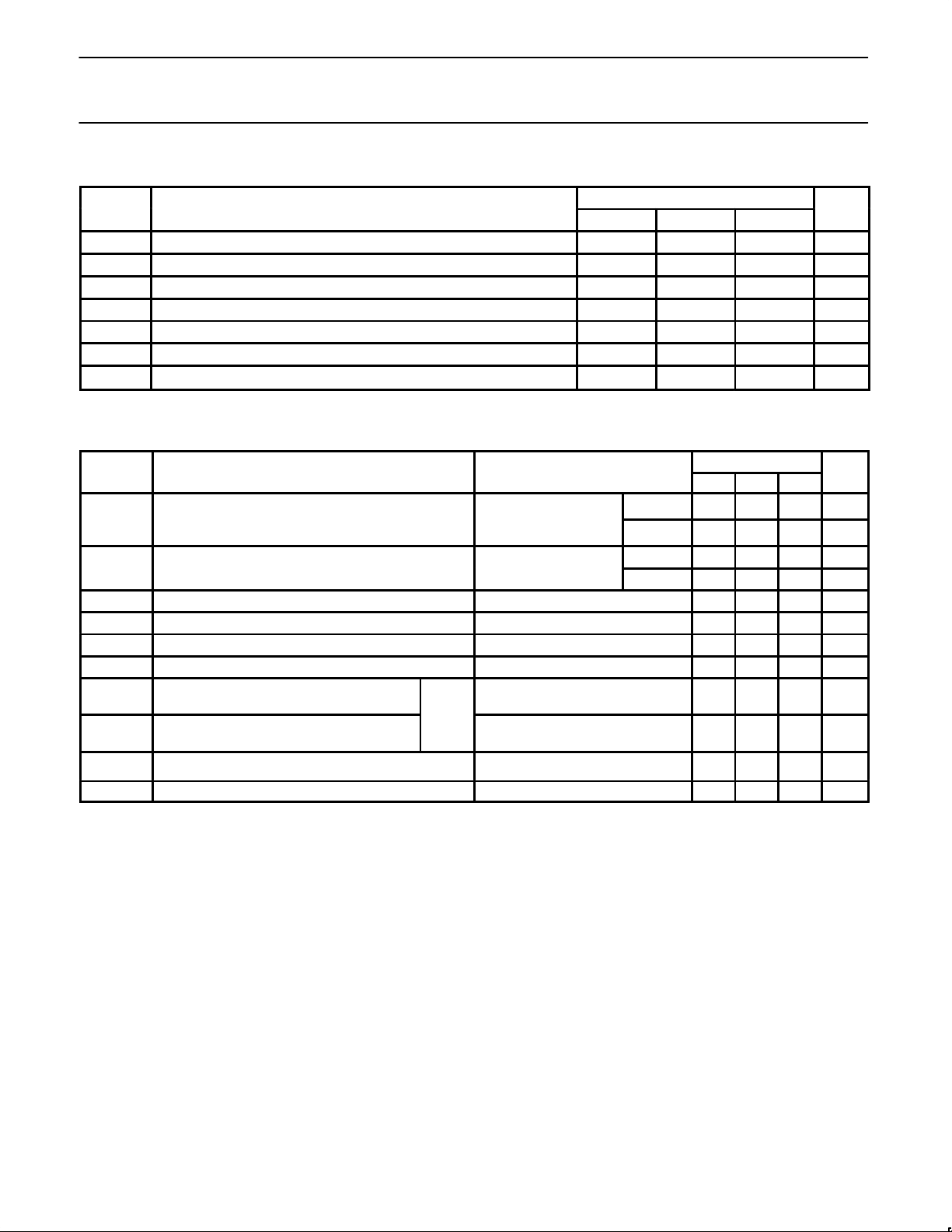
RECOMMENDED OPERATING CONDITIONS
LIMITS
SYMBOL
PARAMETER
MIN NOM MAX UNIT
V
CC
4.5 5.0 5.5 V
V
IH
High–level input voltage 2.0 V
V
IL
Low–level input voltage 0.8 V
I
Ik
Input clamp current –18 mA
I
OH
High–level output current –3 mA
I
OL
Low–level output current 24 mA
T
amb
0 +70
°C
DC ELECTRICAL CHARACTERISTICS
(Over recommended operating free-air temperature range unless otherwise noted.)
SYMBOL PARAMETER TEST LIMITS UNIT
CONDITIONS
1
MIN TYP2MAX
V
OH
High-level output voltage VCC = MIN, VIL = MAX,
±10%V
CC
2.4 V
VIH = MIN, IOH = MAX
±5%V
CC
2.7 3.4 V
V
OL
Low-level output voltage VCC = MIN, VIL = MAX, ±10%V
CC
0.35 0.50 V
VIH = MIN, IOL = MAX ±5%V
CC
0.35 0.50 V
V
IK
Input clamp voltage VCC = MIN, II = I
IK
–0.73 -1.2 V
I
I
Input current at maximum input voltage VCC = MAX, VI = 7.0V 100 µA
I
IH
High–level input current VCC = MAX, VI = 2.7V 20 µA
I
IL
Low–level input current VCC = MAX, VI = 0.5V –20 µA
I
OZH
+ I
IH
VCC = MAX, V
O
= 2.7V 50
µA
I
OZL
+ I
IL
VCC = MAX, VO = 0.5V –50
µA
I
OS
Short–circuit output current
3
VCC = MAX -60 -150 mA
I
CC
Supply current (total) VCC = MAX 155 210 mA
Notes to DC electrical characteristics
1. For conditions shown as MIN or MAX, use the appropriate value specified under recommended operating conditions for the applicable type.
2. All typical values are at VCC = 5V, T
amb
= 25°C.
3. Not more than one output should be shorted at a time. For testing I
OS
, the use of high-speed test apparatus and/or sample-and-hold
techniques are preferable in order to minimize internal heating and more accurately reflect operational values. Otherwise, prolonged shorting
of a high output may raise the chip temperature well above normal and thereby cause invalid readings in other parameter tests. In any
sequence of parameter tests, I
OS
tests should be performed last.
Supply voltage
Operating free air temperature
Off–state output current,
high–level voltage applied
Off–state output current,
low–level voltage applied
An, Bn
Page 6
Philips Semiconductors FAST Products Product specification
FAST 74F807
Octal shift/count registered transceiver
with adder and parity (3–State)
June 18, 1991
6
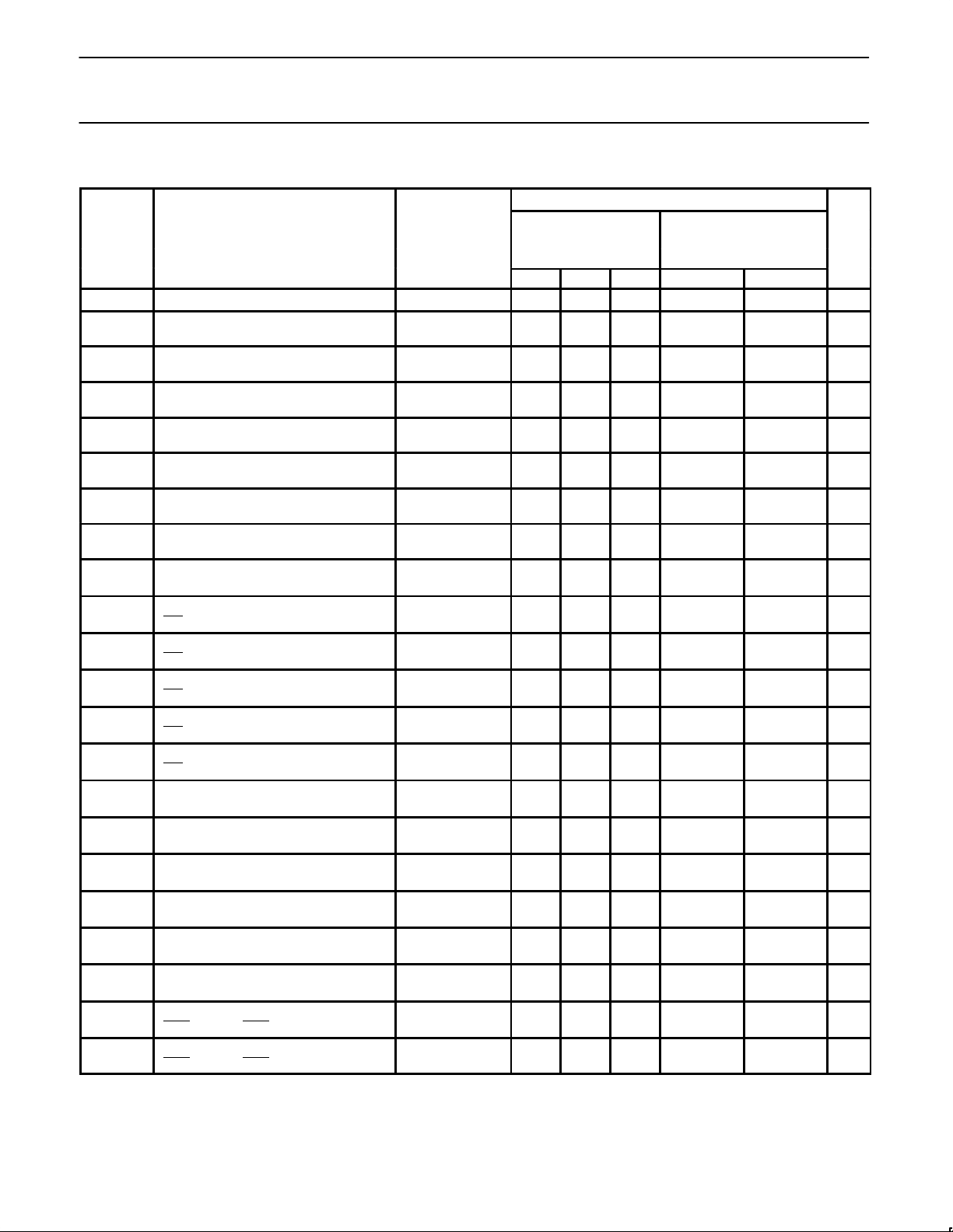
AC ELECTRICAL CHARACTERISTICS
LIMITS
T
amb
= +25°C T
amb
= 0°C to +70°C
SYMBOL PARAMETER TEST VCC = +5.0V
VCC = +5.0V ± 10%
UNIT
CONDITION
CL = 50pF, RL = 500Ω CL = 50p, RL = 500Ω
MIN TYP MAX MIN MAX
f
max
Maximum clock frequency Waveform 1 100 115 70 MHz
t
PLH
t
PHL
Propagation delay
CP to An or Bn (load)
Waveform 1
9.0
5.0
10.5
6.5
11.5
9.5
8.0
4.5
13.5
10.0
ns
t
PLH
t
PHL
Propagation delay
CP to An or Bn (shift)
Waveform 1
9.0
4.5
10.5
6.5
12.5
9.5
8.0
4.5
15.0
10.0
ns
t
PLH
t
PHL
Propagation delay
CP to An or Bn (count)
Waveform 1
9.0
5.0
11.5
6.5
14.0
9.5
8.0
4.5
15.5
10.0
ns
t
PLH
t
PHL
Propagation delay
CP to Bn (add)
Waveform 1
9.0
5.0
10.5
6.5
11.5
9.5
8.0
4.5
13.5
10.0
ns
t
PLH
t
PHL
Propagation delay
CP to STATOUT (load A)
Waveform 1
17.5
12.5
19.5
14.5
22.5
17.0
15.5
11.5
26.5
19.0
ns
t
PLH
t
PHL
Propagation delay
CP to STATOUT (shift)
Waveform 1
11.0
7.0
13.0
8.5
15.5
11.5
9.5
6.5
18.0
12.0
ns
t
PLH
t
PHL
Propagation delay
CP to STATOUT (count)
Waveform 1
10.5
6.5
12.0
8.0
15.0
11.0
9.0
6.0
17.0
11.5
ns
t
PLH
t
PHL
Propagation delay
CP to STATOUT (add)
Waveform 1
13.0
8.5
15.0
10.5
18.0
13.0
11.5
8.0
20.5
14.0
ns
t
PHL
Propagation delay
MR
to An or Bn (load A)
Waveform 3 6.5 8.0 11.0 6.0 12.0 ns
t
PHL
Propagation delay
MR
to STATOUT (load A)
Waveform 3 14.0 16.0 18.5 13.0 20.5 ns
t
PHL
Propagation delay
MR
to STATOUT (shift)
Waveform 3 8.5 10.0 12.5 8.0 14.0 ns
t
PHL
Propagation delay
MR
to STATOUT (count)
Waveform 3 8.5 10.0 12.5 8.0 14.0 ns
t
PHL
Propagation delay
MR
to STATOUT (add)
Waveform 3 10.5 12.0 14.5 9.5 16.0 ns
t
PLH
t
PHL
Propagation delay
An to STATOUT (add)
Waveform 4
6.5
8.0
14.0
14.0
23.5
22.5
5.5
7.5
26.5
27.0
ns
t
PLH
t
PHL
Propagation delay
CI/SI/CE to STATOUT
Waveform 4
19.5
21.0
21.5
22.5
24.0
25.5
17.0
20.0
28.0
29.5
ns
t
PLH
t
PHL
Propagation delay
Sn to STATOUT (load A)
Waveform 4
8.0
7.5
10.0
11.5
12.5
15.5
7.0
7.0
14.5
17.0
ns
t
PLH
t
PHL
Propagation delay
Sn to STATOUT (load B)
Waveform 4
6.5
8.0
10.0
12.0
13.0
15.0
5.5
7.0
15.0
16.5
ns
t
PLH
t
PHL
Propagation delay
Sn to STATOUT (add)
Waveform 4
19.0
18.5
21.0
20.0
23.5
23.0
17.0
17.5
27.5
26.0
ns
t
PLH
t
PHL
Propagation delay
Sn to STATOUT (shift)
Waveform 4
6.0
8.0
8.0
9.5
10.5
12.0
5.0
7.0
12.0
13.5
ns
t
PZH
t
PZL
Output enable time,
OEA to An or OEB to Bn
Waveform 6
Waveform 7
2.5
4.0
4.5
5.5
7.0
8.5
2.0
3.5
8.0
9.0
ns
t
PHZ
t
PLZ
Output disable time,
OEA to An or OEB to Bn
Waveform 6
Waveform 7
2.0
3.5
4.5
5.5
7.5
8.5
2.0
3.0
9.0
9.5
ns
Page 7
Philips Semiconductors FAST Products Product specification
FAST 74F807
Octal shift/count registered transceiver
with adder and parity (3–State)
June 18, 1991
7
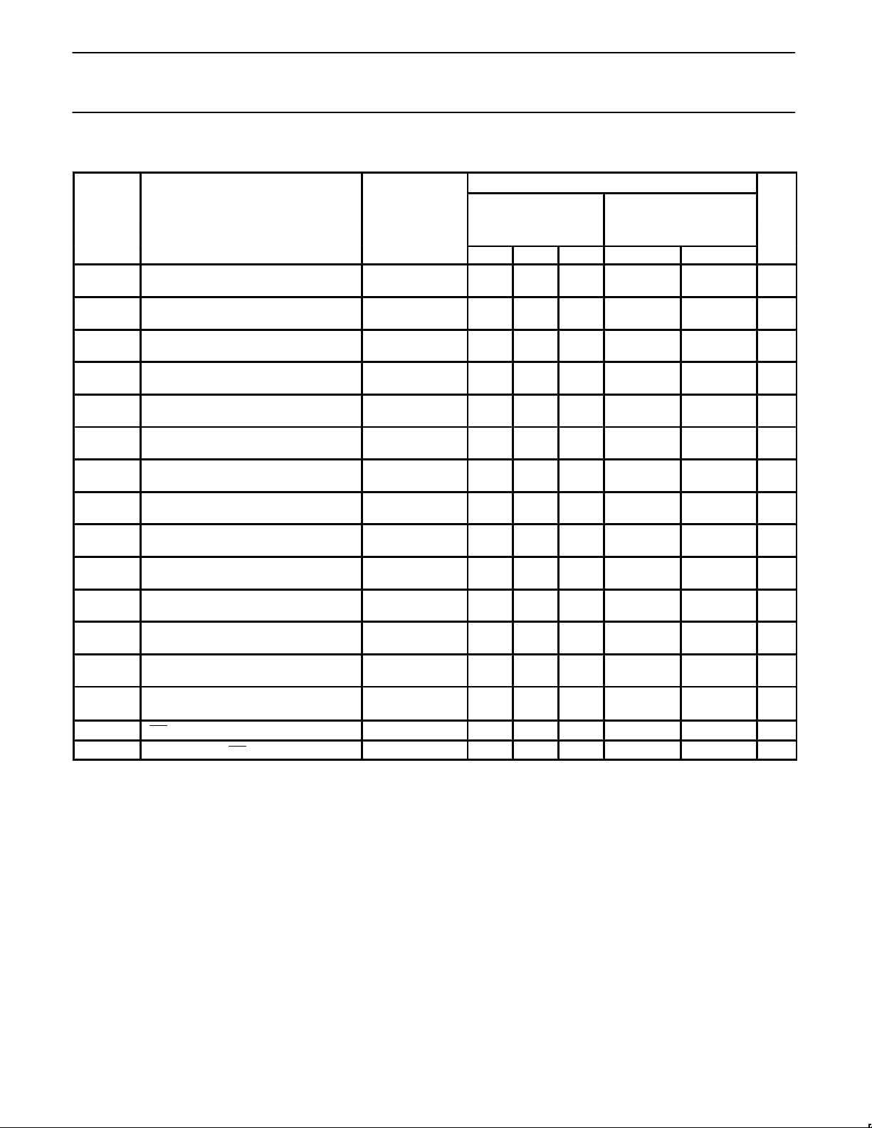
AC SETUP REQUIREMENTS
LIMITS
T
amb
= +25°C T
amb
= 0°C to +70°C
SYMBOL PARAMETER TEST VCC = +5.0V
VCC = +5.0V ± 10%
UNIT
CONDITION
CL = 50pF, RL = 500Ω CL = 50pF, RL = 500Ω
MIN TYP MAX MIN MAX
tsu(H)
t
su
(L)
Setup time, high or low
An, Bn to CP (load)
Waveform 5
6.0
9.5
6.5
12.0
ns
t
h
(H)
t
h
(L)
Hold time, high or low
An, Bn to CP (load)
Waveform 5
0.0
0.0
0.0
0.0
ns
tsu(H)
t
su
(L)
Setup time, high or low
An, Bn to CP (add)
Waveform 5
10.5
16.5
12.0
21.5
ns
t
h
(H)
t
h
(L)
Hold time, high or low
An, Bn to CP (add)
Waveform 5
0.0
0.0
0.0
0.0
ns
tsu(H)
t
su
(L)
Setup time, high or low
Sn to CP (add)
Waveform 5
16.0
16.0
20.0
28.5
ns
tsu(H)
tsu(L)
Setup time, high or low
Sn to CP (count)
Waveform 5
16.5
19.5
19.0
22.5
ns
tsu(H)
t
su
(L)
Setup time, high or low
Sn to CP (shift)
Waveform 5
11.0
7.0
13.0
8.0
ns
tsu(H)
t
su
(L)
Setup time, high or low
Sn to CP (load)
Waveform 5
17.5
6.5
20.5
7.0
ns
t
h
(H)
t
h
(L)
Hold time, high or low
Sn to CP (all modes)
Waveform 5
0.0
0.0
0.0
0.0
ns
tsu(H)
tsu(L)
Setup time, high or low
CI/SI/CE to CP (add)
Waveform 5
10.0
18.0
11.5
22.0
ns
tsu(H)
t
su
(L)
Setup time, high or low
CI/SI/CE to CP (count)
Waveform 5
8.5
16.0
10.0
18.5
ns
tsu(H)
t
su
(L)
Setup time, high or low
CI/SI/CE to CP (shift)
Waveform 5
5.0
9.0
5.5
10.5
ns
t
h
(H)
t
h
(L)
Hold time, high or low
CI/SI/CE to CP (all modes)
Waveform 5
0.0
0.0
0.0
0.0
ns
tw(H)
t
w
(L)
CP pulse width,
High or low
Waveform 1
5.5
4.5
6.0
4.5
ns
tw(L) MR pulse width, low Waveform 3 4.5 5.0 ns
t
rec
Recovery time, MR to CP Waveform 2 2.0 2.0 ns
Page 8
Philips Semiconductors FAST Products Product specification
FAST 74F807
Octal shift/count registered transceiver
with adder and parity (3–State)
June 18, 1991
8
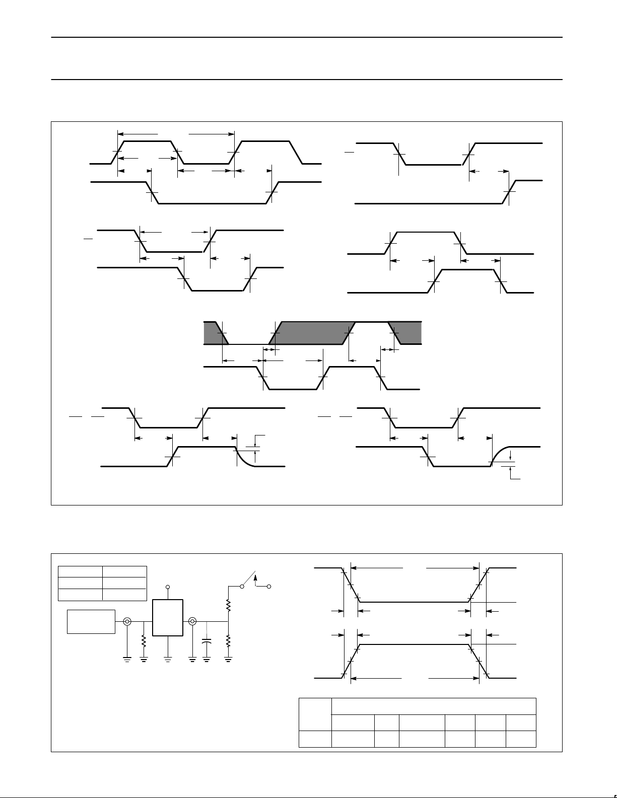
AC WAVEFORMS
V
M
V
M
V
M
V
M
Waveform 4. Propagation delay for select to ST ATOUT, CI/SI/CE
to STATOUT or data to STATOUT
Waveform 5. Data setup and hold times
Waveform 6. 3–State output enable time to high level
and output disable time from high level
Waveform 7. 3-state output enable time to low level
and output disable time from low level
V
M
V
M
VMV
M
V
M
V
M
tsuL)
t
su
(H)
th(L) th(H)
V
M
V
M
V
M
t
PHZ
t
PZH
VOH -0.3V
0V
V
M
V
M
V
M
t
PLZ
t
PZL
VOL +0.3V
OEB or OEA
Bn or An
An, Bn, Sn,
CI/SI/CE
STATOUT
t
PLH
t
PHL
V
M
tw(L)
V
M
V
M
V
M
Waveform 2. Master reset to clock recovery time
CP
t
rec
An, Sn,
CI/SI/CE
OEB
or OEA
Bn or An
V
M
V
M
V
M
V
M
Waveform 3. Propagation delay for master reset to data
or master reset to STATOUT
MR
t
PHL
t
PLH
Bn or An
STATOUT
tw(L)
MR
CP
Waveform 1. Propagation delay for clock input to output,
clock pulse width, and maximum clock frequency
CPBA
or
CPAB
V
M
V
M
V
M
tw(H)
1/f
max
V
M
V
M
t
PLH
tw(L)
t
PHL
An or Bn
STATOUT
Notes to AC waveforms
1. For all waveforms, V
M
= 1.5V.
2. The shaded areas indicate when the input is permitted to change for predictable output performance.
TEST CIRCUIT AND WAVEFORMS
t
w
90%
V
M
10%
90%
V
M
10%
90%
V
M
10%
90%
V
M
10%
NEGATIVE
PULSE
POSITIVE
PULSE
t
w
AMP (V)
0V
0V
t
THL (tf
)
INPUT PULSE REQUIREMENTS
rep. rate
t
w
t
TLHtTHL
1MHz 500ns 2.5ns
2.5ns
Input pulse definition
V
CC
family
74F
D.U.T.
PULSE
GENERATOR
R
L
C
L
R
T
V
IN
V
OUT
Test circuit for 3–State outputs
DEFINITIONS:
R
L
= Load resistor; see AC electrical characteristics for
value.
C
L
= Load capacitance includes jig and probe
capacitance; see AC electrical characteristics for
value
R
T
= Termination resistance should be equal to Z
OUT
of
pulse generators.
t
THL (tf
)
t
TLH (tr
)
t
TLH (tr
)
AMP (V)
amplitude
3.0V
1.5V
V
M
R
L
7.0V
SWITCH POSITION
TEST SWITCH
closed
openAll other
t
PLZ
, t
PZL
.
 Loading...