

Page 1
© 1999 Fairchild Semiconductor Corporation DS009588 www.fairchildsemi.com
April 1988
Revised August 1999
74F676 16-Bit Serial/Parallel-In, Serial-Out Shift Register
74F676
16-Bit Serial/Parallel-In, Serial-Out Shift Register
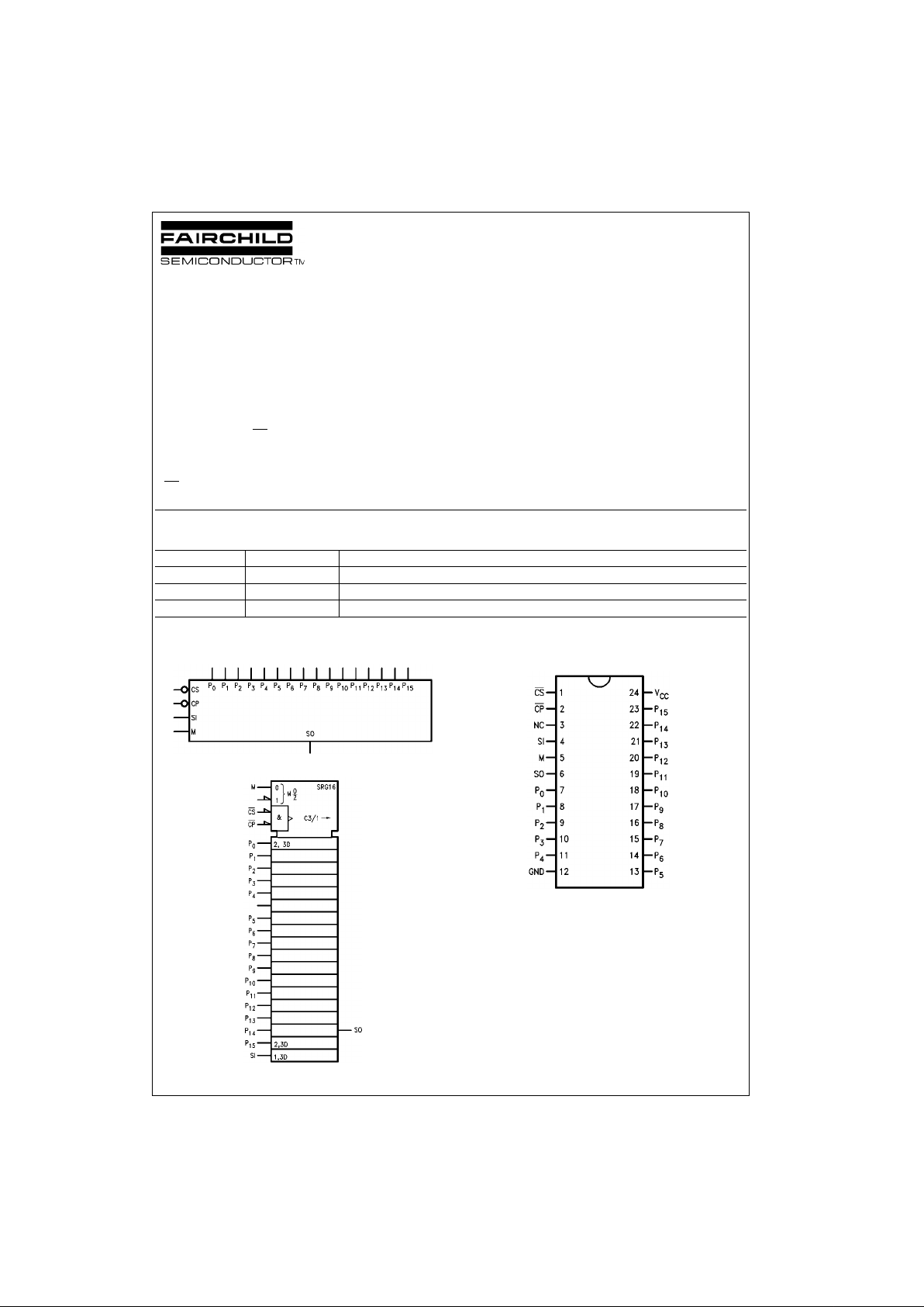
General Description
The 74F676 contains 16 fl ip-flops with provision for synchronous parallel or serial entry and serial output . When
the Mode (M) input is HIGH, information present on the
parallel data (P
0–P15
) inputs is entered on the falling edge
of the Clock Pulse (CP
) input signal. When M is LOW, data
is shifted out of the most significant bit p osition while info rmation present on the Ser ial (SI) input shi fts into the le ast
significant bit position. A H IGH signal on the Chip Select
(CS
) input prevents both parallel and serial operations.
Features
■ 16-bit parallel-to-serial conversion
■ 16-bit serial-in, serial-out
■ Chip select control
■ Slim 24 lead 300 mil package
Ordering Code:
Devices also availab le in Tape and Reel. Specify by appending th e s uffix let t er “X” to the ordering code.
Logic Symbols
IEEE/IEC
Connection Diagram
Order Number Package Number Package Description
74F676SC M24B 28-Lead Small Outline Integrated Circuit (SOIC), JEDEC MS-013, 0.300 Wide
74F676PC N24A 24-Lead Plastic Dual-In-Line Package (PDIP), JEDEC MS-010, 0.600 Wide
74F676SPC N24C 24-Lead Plastic Dual-In-Line Package (PDIP), JEDEC MS-100, 0.300 Wide
Page 2
www.fairchildsemi.com 2
74F676
Unit Loading/Fan Out
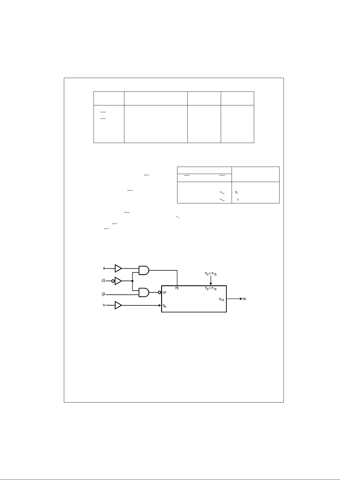
Functional Description
The 16-bit shift register o per ate s in one of thr ee m ode s, as
indicated in the Shift Register Operations Table.
HOLD— a HIGH signal on the Ch ip Select ( CS
) input pre-
vents clocking, and data is stored in the sixteen registers.
Shift/Serial Load— data present on the SI pin shifts into
the register on the falling edge of CP
. Data enters the Q
0
position and shifts toward Q15 on successive clocks, finally
appearing on the SO pin.
Parallel Load— data present on P
0–P15
are entered into
the register on the falling edge of CP
. The SO output repre-
sents the Q
15
register output.
To prevent false cloc king, CP
must be LOW during a LOW-
to-HIGH transition of CS
.
Shift Register Operations Table
H = HIGH Voltage Level
L = LOW Voltage Level
X = Immaterial
= HIGH-to-LOW Tran s iti on
Block Diagram
Pin Names Description
U.L.
Input I
IH/IIL
HIGH/LOW
Output I
OH/IOL
P0–P
15
Parallel Data Inputs 1.0/1.0 20 µA/−0.6 mA
CS
Chip Select Input (Active LOW) 1.0/1.0 20 µA/−0.6 mA
CP
Clock Pulse Input (Active LOW) 1.0/1.0 20 µA/−0.6 mA
M Mode Select Input 1.0/1.0 20 µA/−0.6 mA
SI Serial Data Input 1.0/1.0 20 µA/−0.6 mA
SO Serial Output 50/33.3 −1 mA/20 mA
Control Input
Operating Mode
CS
MCP
HXXHold
LL
Shift/Serial Load
LH
Parallel Load
Page 3

3 www.fairchildsemi.com
74F676
Absolute Maximum Ratings(Note 1) Recommended Operating
Conditions
Note 1: Absolute maximum ratings are values beyon d which the device
may be damaged or have its useful life impaired . Functional operation
under these condit ions is not implied.
Note 2: Either voltage limit or curren t limit is sufficient to protect in puts.
DC Electrical Characteristics
Storage Temperature −65°C to +150°C
Ambient Temperature under Bias −55°C to +125°C
Junction Temperature under Bias −55°C to +150°C
V
CC
Pin Potential to Ground Pin −0.5V to +7.0V
Input Voltage (Note 2) −0.5V to +7.0V
Input Current (Note 2) −30 mA to +5.0 mA
Voltage Applied to Output
in HIGH State (with V
CC
= 0V)
Standard Output −0.5V to V
CC
3-STATE Output −0.5V to +5.5V
Current Applied to Output
in LOW State (Max) twice the rated I
OL
(mA)
Free Air Ambi ent Temperat ure 0°C to +70°C
Supply Voltage +4.5V to +5.5V
Symbol Parameter Min Typ Max Units
V
CC
Conditions
V
IH
Input HIGH Voltage 2.0 V Recognized as a HIGH Signal
V
IL
Input LOW Voltage 0.8 V Recognized as a LOW Signal
V
CD
Input Clamp Diode Voltage −1.2 V Min IIN = −18 mA
V
OH
Output HIGH 10% V
CC
2.5
VMin
IOH = −1 mA
Voltage 5% V
CC
2.7 IOH = −1 mA
V
OL
Output LOW
10% V
CC
0.5 V Min IOL = 20 mA
Voltage
I
IH
Input HIGH
5.0 µAMaxVIN = 2.7V
Current
I
BVI
Input HIGH Current
7.0 µAMaxVIN = 7.0V
Breakdown Test
I
CEX
Output HIGH
50 µAMaxV
OUT
= V
CC
Leakage Current
V
ID
Input Leakage
4.75 V 0.0
IID = 1.9 µA,
Test All Other Pins Grounded
I
OD
Output Leakage
3.75 µA0.0
V
IOD
= 150 mV,
Circuit Current All Other Pins Grounded
I
IL
Input LOW Current −0.6 mA Max VIN = 0.5V
I
OS
Output Short-Circuit Current −60 −150 mA Max V
OUT
= 0V
I
CC
Power Supply Current 72 mA Max
Page 4

www.fairchildsemi.com 4
74F676
AC Electrical Characteristics
AC Operating Requirements
Symbol Parameter
TA = +25°CT
A
= −55°C to 125°CTA = 0°C to +70°C
Units
VCC = +5.0V VCC = +5.0V VCC = +5.0V
CL = 50 pF CL = 50 pF CL = 50 pF
Min Typ Max Min Max Min Max
f
MAX
Maximum Clock Frequency 100 110 45 90 MHz
t
PLH
Propagation Delay 4.5 9.0 11.0 4.5 17.0 4.5 12.0
ns
t
PHL
CP to SO
5.0 9.0 12.5 5.0 14.5 5.0 13.5
Symbol Parameter
TA = +25°CTA = −55°C to 125°CTA, VCC = ____
UnitsVCC = +5.0V VCC = +5.0V VCC = +5.0V
Min Max Min Max Min Max
tS(H) Setup Time, HIGH or LOW 4.0 4.0 4.0
tS(L)
SI to CP
4.0 4.0 4.0
ns
tH(H) Hold Time, HIGH or LOW 4.0 4.0 4.0
tH(L)
SI to CP
4.0 4.0 4.0
tS(H) Setup Time, HIGH or LOW 3.0 3.0 3.0
tS(L)
Pn to CP
3.0 3.0 3.0
ns
tH(H) Hold Time, HIGH or LOW 4.0 4.0 4.0
tH(L)
Pn to CP
4.0 4.0 4.0
tS(H) Setup Time, HIGH or LOW 8.0 8.0 8.0
tS(L)
M to CP
8.0 8.0 8.0
ns
tH(H) Hold Time, HIGH or LOW 2.0 2.0 2.0
tH(L)
M to CP
2.0 2.0 2.0
tS(L) Setup Time, LOW
10.0 12.0 10.0
CS to CP
ns
tH(H) Hold Time, HIGH
10.0 10.0 10.0
CS to CP
tW(H)
CP Pulse Width
4.0 5.0 4.0
ns
tW(L) HIGH or LOW 6.0 9.0 6.0
Page 5

5 www.fairchildsemi.com
74F676
Physical Dimensions inches (millimeters) unless otherwise noted
28-Lead Small Outline Integrated Circuit (SOIC), JEDEC MS-013, 0.300 Wide
Package Number M24B
24-Lead Plastic Dual-In-Line Package (PDIP), JEDEC MS-010, 0.600 Wide
Package Number N24A
Page 6

www.fairchildsemi.com 6
74F676 16-Bit Serial/Parallel-In, Serial-Out Shift Register
Physical Dimensions inches (millimeters) unless otherwise noted (Continued)
24-Lead Plastic Dual-In-Line Package (PDIP), JEDEC MS-100, 0.300 Wide
Package Number N24C
Fairchild does not assume any responsibility for use of any circuitry described, no circuit pate nt licenses are implied and
Fairchild reserves the right at any time without notice to change said circuitry and specifications.
LIFE SUPPORT POLICY
FAIRCHILD’S PRODUCTS ARE NOT AUTHORIZED FOR USE AS CRITICAL COMPONENTS IN LIFE SUPPORT
DEVICES OR SYSTEMS WITHOUT THE EXPRESS WRITTEN APPROVAL OF THE PRESIDENT OF FAIRCHILD
SEMICONDUCTOR CORPORATION. As used herein:
1. Life support devices or systems are devices or syste ms
which, (a) are intended for surgical implant into the
body, or (b) support or sustain life, and (c) whose failure
to perform when properly used in accordance with
instructions for use provided in the labeling, can be reasonably expected to result in a significant inju ry to the
user.
2. A critical component i n any compon ent of a lif e support
device or system whose failu re to perform can be reasonably expected to ca use the fa i lure of the life su pp ort
device or system, or to affect its safety or effectiveness.
www.fairchildsemi.com
 Loading...