

Page 1
April 1988
Revised March 1999
74F583 4-Bit BCD Adder
© 1999 Fairchild Semiconductor Corporation DS009570.prf www.fairchildsemi.com
74F583
4-Bit BCD Adder
General Description
The ’F583 high-speed 4-bit, BCD full adder with internal
carry lookahead accep ts two 4-bit decimal numbers (A
0
–
A
3
, B0–B3) and a Carry Input (Cn). It generates the decimal
sum outputs (S
0–S3
), and a Carry Out put (C
n+4
) if the sum
is greater than 9. The 'F583 is the functional equ ivalent of
the 82S83.
Features
■ Adds two decimal numbers
■ Full internal lookahead
■ Fast ripple carry for economical expansion
■ Sum output delay time 16.5 ns max
■ Ripple carry delay time 8.5 ns max
■ Input to ripple delay time 14.0 ns max
■ Supply current 60 mA max
Ordering Code:
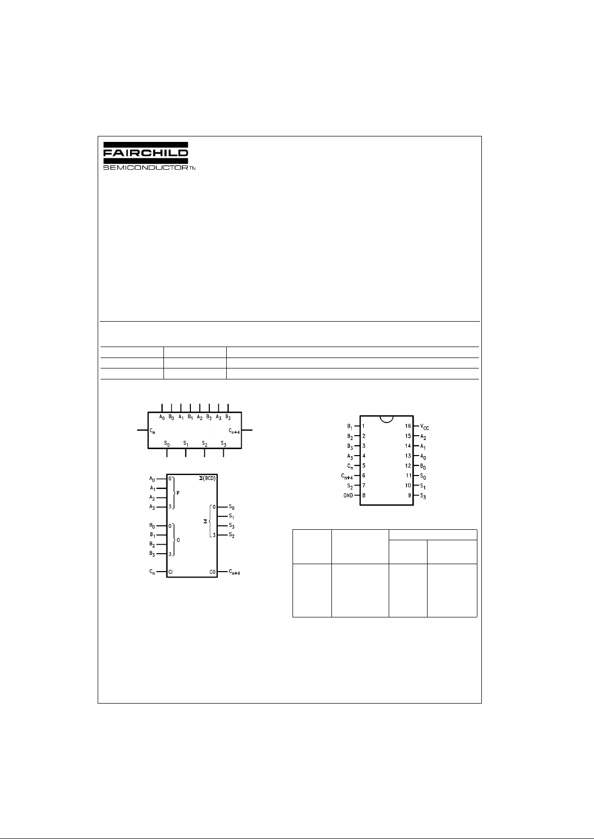
Logic Symbols
IEEE/IEC
Connection Diagram
Unit Loading/Fan Out
Order Number Package Number Package Description
74F583SC M16B 16-Lead Small Outline Intergrated Circuit (SOIC), JEDEC MS-013, 0.300 Wide
74F583PC N16E 16-Lead Plastic Dual-In-Line Package (PDIP), JEDEC MS-001, 0.300 Wide
74F
Pin
Names
Description U.L. Input I
IH/IIL
HIGH/LOW Output IOH/I
OL
A0–A
3
A Operand Inputs 1.0/2.0 20 µA/−1.2 mA
B
0–B3
B Operand Inputs 1.0/2.0 20 µA/−1.2 mA
C
n
Carry Input 1.0/1.0 20 µA/−0.6 mA
S
0–S3
Sum Outputs 50/33.3 −1 m A/20 mA
C
n+4
Carry Output 50/33.3 −1 mA/20 mA
Page 2
www.fairchildsemi.com 2
74F583
Functional Description
The ’F583 4-bit binary coded (BCD) full adder performs the
addition of two deci mal num bers (A
0–A3
, B0–B3). The loo-
kahead generates the BCD carry terms internally, allowing
the 'F583 to then do BCD addition correctly. For BCD numbers 0 through 9 at A a nd B inputs, the B CD sum forms at
the output. In the addition of two BCD numbers totalling a
number greater than 9, a valid BCD number and a carry will
result.
For input values larger than 9, the number is converted
from binary to BCD. Binary to BCD conver sion occurs by
grounding one set of inputs, A
n
or Bn, and applying any 4-
bit binary number to the other set of inpu ts. If the input is
between 0 and 9, a BC D number occurs at the ou tput. If
the binary input falls b etween 10 and 15, a carry term is
generated. Both the carry term and the sum are the BCD
equivalent of the binary i nput. Converting binar y numbers
greater than 16 may be achieved through cascading
'F583s.
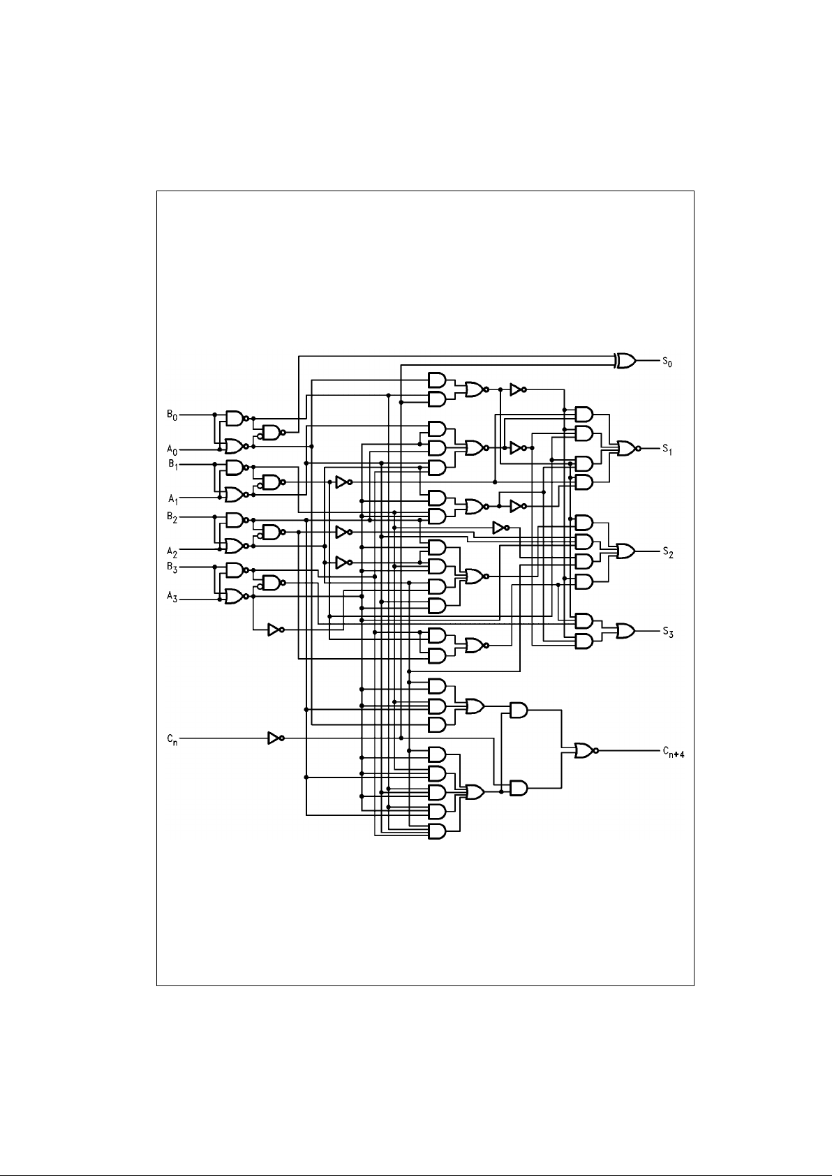
Logic Diagram
Please note that this diagram is provided only for the understan ding of logic operation s and should not be used t o es t im ate propagation delays.
Page 3
3 www.fairchildsemi.com
74F583
Absolute Maximum Ratings(Note 1) Recommended Operating
Conditions
Note 1: Absolute maximum ratings are values beyon d which the device
may be damaged or have its useful life impaired . Functional operation
under these condit ions is not implied.
Note 2: Either voltage limit or curren t limit is sufficient to protec t in puts.
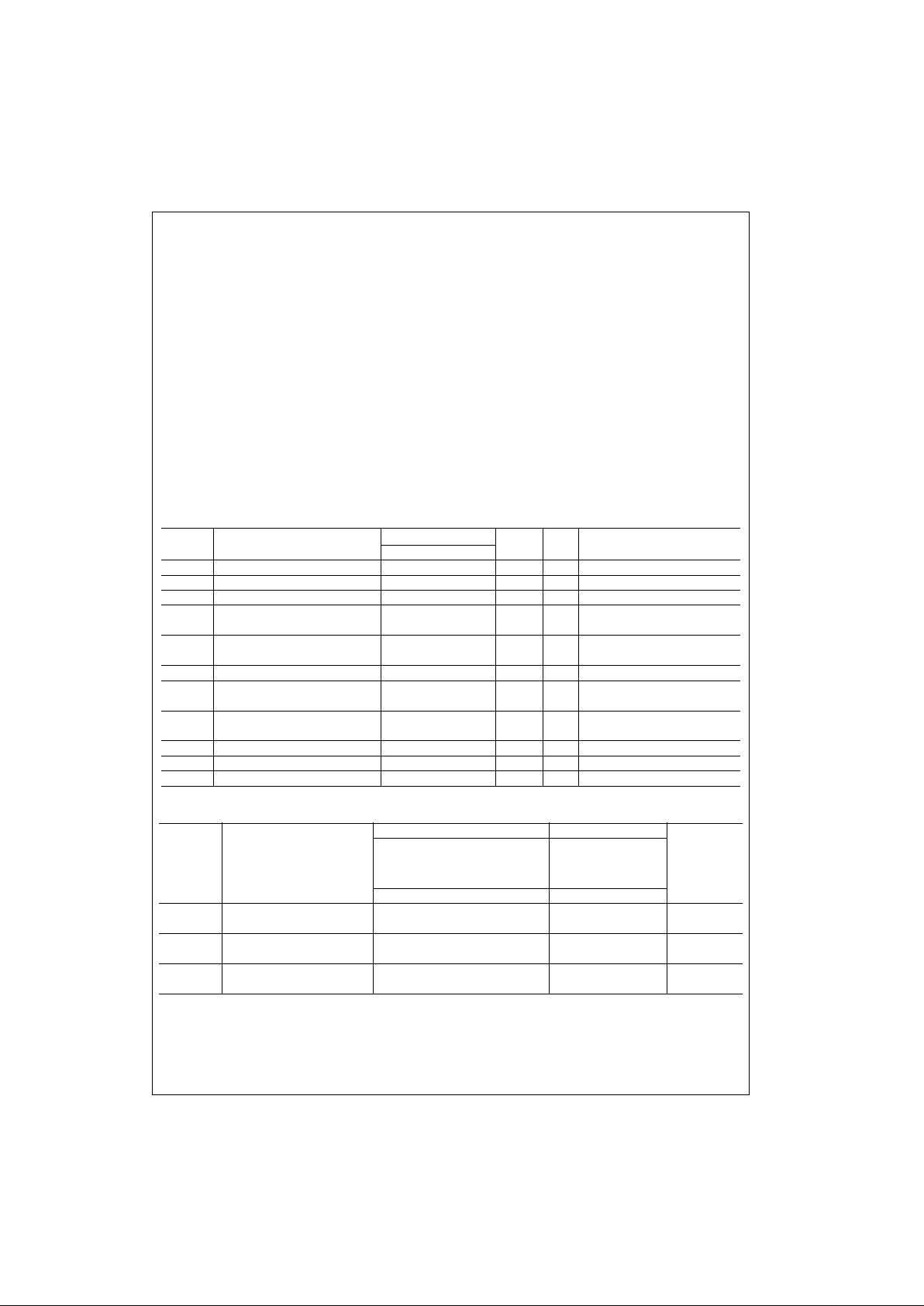
DC Electrical Characteristics
AC Electrical Characteristics
Storage Temperature −65°C to +150°C
Ambient Temperature under Bias −55°C to +125°C
Junction Temperature under Bias −55°C to +175°C
Plastic −55°C to +150°C
V
CC
Pin Potential to
Ground Pin −0.5V to +7.0V
Input Voltage (Note 2) −0.5V to +7.0V
Input Current (Note 2) −30 mA to +5.0 mA
Voltage Applied to Output
in HIGH State (with V
CC
= 0V)
Standard Output −0.5V to V
CC
3-STATE Output −0.5V to +5.5V
Current Applied to Output
in LOW State (Max)
twicetheratedI
OL
(mA)
Free Air Ambi ent Temper ature
Commercial 0°C to +70°C
Supply Voltage
Commercial +4.5V to +5.5V
Symbol Parameter
74F
Units
V
CC
Conditions
Min Typ Max
V
IH
Input HIGH Voltage 2.0 V Recognized as a HIGH Signal
V
IL
Input LOW Voltage 0.8 V Recognized as a LOW Signal
V
CD
Input Clamp Diode Voltage −1.2 V Min IIN = −18 mA
V
OH
Output HIGH 74F 10% V
CC
2.5 V Min IOH = −1 mA
Voltage 74F 5% V
CC
2.7 IOH = −1 mA
V
OL
Output LOW 74F 10% V
CC
0.5 V Min IOL = 20 mA
Voltage
I
IH
Input HIGH Current 20 µAMaxVIN = 2.7V
I
BVI
Input HIGH Current 100 µAMaxVIN = 7.0V
Breakdown Test
I
IL
Input LOW Current −0.6 mA Max VIN = 0.5V (Cn)
−1.2 VIN = 0.5V (An, Bn)
I
OS
Output Short-Circuit Current −60 −150 mA Max V
OUT
= 0V
I
CEX
Output HIGH Leakage Current 250 µAMaxV
OUT
= V
CC
I
CCL
Power Supply Current 40 60 mA Max VO = LOW
74F 74F
TA = +25°CT
A
, VCC = Com
Symbol Parameter VCC = +5.0V CL = 50 pF Units
CL = 50 pF
Min Typ Max Min Max
t
PLH
Propagation Delay 2.5 13.0 16.5 2.5 17.5 ns
t
PHL
An or Bn to S
n
2.5 11.0 14.0 2.5 15.0
t
PLH
Propagation Delay 2.5 6.5 8.5 2.5 9.5 ns
t
PHL
Cn to C
n+4
2.5 5.0 6.5 2.5 7.5
t
PLH
Propagation Delay 4.0 11.0 14.0 4.0 15.0 ns
t
PHL
An or Bn to C
n+4
4.0 8.0 10.5 4.0 11.5
Page 4
www.fairchildsemi.com 4
74F583
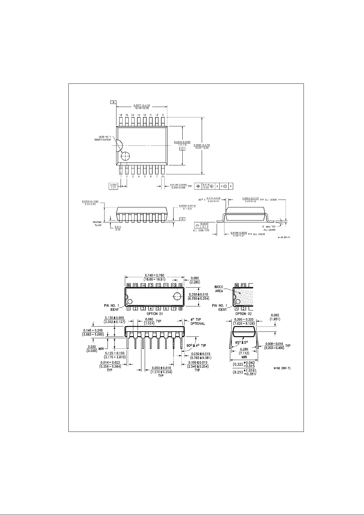
Physical Dimensions inches (millimeters) unless otherwise noted
16-Lead Small Outline Intergrated Circuit (SOIC), JEDEC MS-013, 0.300 Wide
Package Number M16B
16-Lead Plastic Dual-In-Line Package (PDIP), JEDEC MS-001, 0.300 Wide
Package Number N16E
Page 5

Fairchild does not assume any responsibility for use of any circuitry described, no circuit patent licenses are implied and Fairchild reserves the right at any time without notice to change said circuitry and specifications.
74F583 4-Bit BCD Adder
LIFE SUPPORT POLICY
FAIRCHILD’S PRODUCTS ARE NOT AUTHORIZED FOR USE AS CRITICAL COMPONENTS IN LIFE SUPPORT
DEVICES OR SYSTEMS WITHOUT THE EXPRESS WRITTEN APPROVAL OF THE PRESIDENT OF FAIRCHILD
SEMICONDUCTOR CORPORATION. As used herein:
1. Life support devices or systems are de vices o r systems
which, (a) are intended for surgical implant into the
body, or (b) support or sustain life, and (c) whose failure
to perform when properly used in accordance with
instructions for use provide d in the lab el ing , can be re asonably expected to result in a significant in jury to the
user.
2. A critical component in any component of a life support
device or system whose failure to perform can be r easonably expected to cau se th e f ail ur e o f the life sup por t
device or system, or to affect its safety or effectiveness.
www.fairchildsemi.com
 Loading...