

Page 1
© 1999 Fairchild Semiconductor Corporation DS009584 www.fairchildsemi.com
March 1988
Revised August 1999
74F657 Octal Bidirectional Transceiver with
74F657
Octal Bidirectional Transceiver with
8-Bit Parity Generator/Checker and 3-STATE Outputs
General Description
The 74F657 contains eight non-inverting buffers with 3STATE outputs and an 8-bi t parity genera tor/checker. It is
intended for bus-oriented applications. The buffers have a
guaranteed current sinking capability of 24 mA at the A
Port and 64 mA at the B Port.
Features
■ 300 Mil 24-pin slimline DIP
■ Combines 74F245 and 74F280A functions in one
package
■ 3-STATE outputs
■ B Outputs sink 64 mA
■ 12 mA source current, B side
■ Input diodes for termination effects
Ordering Code:
Devices also availab le in Tape and Reel. Specify by appending th e s uffix let t er “X” to the ordering code.
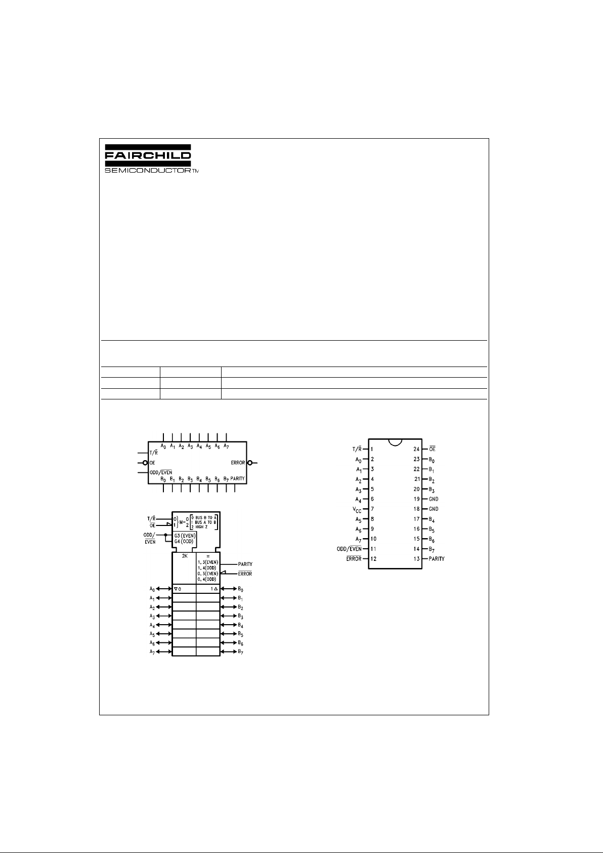
Logic Symbols
IEEE/IEC
Connection Diagram
Order Number Package Number Package Description
75F657SC M24B 24-Lead Small Outline Integrated Circuit (SOIC), JEDEC MS-013, 0.300 Wide
74F657SPC N24C 24-Lead Plastic Dual-In-Line Package (PDIP), JEDEC MS-100, 0.300 Wide
Page 2
www.fairchildsemi.com 2
74F657
Unit Loading/Fan Out
Functional Description
The Transmit/Receive (T/R) input determines the direction
of the data flow through the bidirectional transceivers.
Transmit (active HIGH) enables data from the A Port to the
B Port; Receive (active LOW) enables data from the B Port
to the A Port.
The Output Enable (OE
) input disables the parity and
ERROR
outputs and both the A and B Ports by pl acing
them in a HIGH-Z co ndition when the O utput En able input
is HIGH.
When transmitting (T/R
HIGH), the parity generator detects
whether an even or odd numbe r of bits on the A Port ar e
HIGH and compares these wi th the condition of the pa rity
select (ODD/EVEN
). If the Parity Select is HIGH and an
even number of A inputs are HIGH, the Parity output is
HIGH.
In receiving mode (T/R
LOW), the parity select and number
of HIGH inputs on port B a re compar ed to the condi tion of
the Parity input. If an even number of bits on the B Port are
HIGH, the parity select is HIGH, and the PARITY input is
HIGH, then ERROR
will be HIGH to indicate no error. If an
odd number of bits on the B Port are HIGH, the parity
select is HIGH, and the PARITY input is HIGH, the ERROR
will be LOW indicating an error.
Function Table
H = HIGH Voltage Level
L = LOW Voltage Level
X = Immaterial
Z = High Impedance
Function Table
H = HIGH Voltage Level
L = LOW Voltage Level
X = Immaterial
Pin Names Description
U.L.
Input I
IH/IIL
HIGH/LOW
Output I
OH/IOL
A0–A
7
Data Inputs/ 4.5/0.15 90 µA/− 90 µA
3-STATE Outputs 150/40 (33.3) −3 mA/24 mA (20 mA)
B
0–B7
Data Inputs/ 3.5/0.117 70 µA/−70 µA
3-STATE Outputs 600/106.6 (80) −12 mA/64 mA (48 mA)
T/R
Transmit/Receive Input 2.0/0.067 40 µA/−40 µA
OE
Enable Input 2.0/0.067 40 µA/−40 µA
PARITY Parity Input/ 3.5/0.117 70 µA/−70µA
3-STATE Output 600/106.6 (80) −12 mA/64 mA (48 mA)
ODD/EVEN
ODD/EVEN Parity Input 1.0/0.033 20 µA/−20 µA
ERROR
Error Output 600/106.6 (80) −12 mA/64 mA (48 mA)
Number of
Inputs that
are HIGH
Inputs
Input/
Outputs
Output
OE
T/R
ODD/
Parity ERROR
Outputs
EVEN
Mode
0, 2, 4, 6, 8 L H H H Z Transmit
LH L L Z Transmit
LL H H H Receive
LL H L L Receive
LL L H L Receive
LL L L H Receive
1, 3, 5, 7 L H H L Z Transmit
LH L H Z Transmit
LL H H L Receive
LL H L H Receive
LL L H H Receive
LL L L L Receive
Immaterial H X X Z Z Z
Inputs
Outputs
OE
T/R
L L Bus B Data to Bus A
L H Bus A Data to Bus B
H X High-Z State
Page 3
3 www.fairchildsemi.com
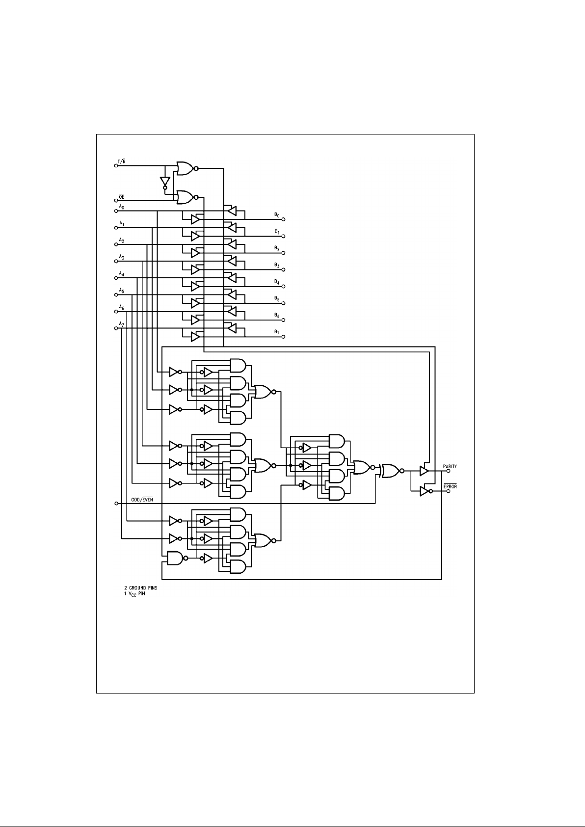
74F657
Functional Block Diagram
Page 4

www.fairchildsemi.com 4
74F657
Absolute Maximum Ratings(Note 1) Recommended Operating
Conditions
Note 1: Absolute maximum ratings are values beyond which the device
may be damaged or have its useful life impaired. Functional operation
under these conditi ons is not implied.
Note 2: Either voltage limit or curren t limit is sufficient to protect in put s .
DC Electrical Characteristics
Storage Temperature −65°C to +150°C
Ambient Temperature under Bias −55°C to +125°C
Junction Temperature under Bias −55°C to +150°C
V
CC
Pin Potential to Ground Pin −0.5V to +7.0V
Input Voltage (Note 2) −0.5V to +7.0V
Input Current (Note 2) −30 mA to +5.0 mA
Voltage Applied to Output
in HIGH State (with V
CC
= 0V)
Standard Output −0.5V to V
CC
3-STATE Output −0.5V to +5.5V
Current Applied to Output
in LOW State (Max) twice the rated I
OL
(mA)
Free Air Ambient Temperature 0°C to +70°C
Supply Voltage +4.5V to +5.5V
Symbol Parameter Min Typ Max Units
V
CC
Conditions
V
IH
Input HIGH Voltage 2.0 V Recognized as a HIGH Signal
V
IL
Input LOW Voltage 0.8 V Recognized as a LOW Signal
V
CD
Input Clamp Diode Voltage −1.2 V Min IIN = −18 mA
V
OH
Output HIGH 10% V
CC
2.5
VMin
IOH = −1 mA (An)
Voltage 10% V
CC
2.4
IOH = −3 mA (An Bn, Parity, ERROR)
10% V
CC
2.0
IOH = −15 mA (Bn, Parity, ERROR)
5% V
CC
2.7 IOH = −1 mA (An)
5% V
CC
2.7
IOH = −3 mA (An, Bn, Parity, ERROR)
V
OL
Output LOW 10% V
CC
0.5
VMin
IOL = 24 mA (An)
Voltage 10% V
CC
0.55
IOL = 64 mA (Bn Parity, ERROR)
I
IH
Input HIGH 20
µAMax
VIN = 2.7V (ODD/EVEN)
Current 40
VIN 2.7V (T/R, OE)
I
BVI
Input HIGH Current
100 µAVCC = 0VIN = 7.0V (T/R, OE, ODD/EVEN)
Breakdown Test
I
BVIT
Input HIGH Current 1.0
mA Max
VIN = 5.5V (Parity, Bn)
Breakdown Test (I/O) 2.0 VIN = 5.5V (An)
I
IL
Input LOW −20
µAMax
VIN = 0.5V (ODD/EVEN)
Current −40
VIN = 0.5V (T/R, OE)
I
OZH
Output Leakage Current 50 µAMax
V
OUT
= 2.7V (ERROR)
I
OZL
Output Leakage Current −50 µAMaxV
OUT
= 0.5V (ERROR)
IIH + I
OZH
Output Leakage 70
µAMax
V
I/O
= 2.7V (Bn, Parity)
Current 90 V
I/O
= 2.7V (An)
IIL + I
OZL
Output Leakage −70
µAMax
V
I/O
= 0.5V (Bn, Parity)
Current −90 V
I/O
= 0.5V (An)
I
OS
Output Short-Circuit −60 −150
mA Max
V
OUT
= 0V (An)
Current −100 −225
V
OUT
= 0V (Bn, Parity, ERROR)
I
CEX
Output HIGH Leakage 250 µAMax
V
OUT
= VCC (ERROR)
Current 1.0 mA Max V
OUT
= VCC (Bn, Parity)
2.0 mA Max V
OUT
= VCC (An)
I
ZZ
Bus Drainage Test 500 µA0.0VV
OUT
= 5.25V (An, Bn, Parity, ERROR)
I
CCH
Power Supply Current 101 125 mA Max VO = HIGH
I
CCL
Power Supply Current 112 150 mA Max VO = LOW
I
CCZ
Power Supply Current 109 145 mA Max VO = HIGH Z
Page 5

5 www.fairchildsemi.com
74F657
AC Electrical Characteristics
Note 3: These delay times reflect the 3-S TATE recovery time only and not the sign al time thro ugh the bu ffers or the par ity check circ uity. To assure VALID
information at the ER R OR
pin, time must be allowed for the signal to propagate through the drivers (B to A), through t he parity check circuitry (s ame as A to
PARITY), and to the ERROR
output after the ERROR pin has been enabled (Output Enable times). VALID data at the ERROR pin ≥ (A to PARITY) + (Output
Enable Time).
Symbol Parameter
TA = +25°CT
A
= −55°C to +125°CTA = 0°C to +70°C
Units
VCC = +5.0V VCC = +5.0V VCC = +5.0V
CL = 50 pF CL = 50 pF CL = 50 pF
Min Typ Max Min Max Min Max
t
PLH
Propagation Delay 2.5 4.5 8.0 2.5 9.5 2.5 9.0
ns
t
PHL
An to Bn, Bn to A
n
3.0 4.9 7.5 3.0 8.5 3.0 8.0
t
PLH
Propagation Delay 6.5 10.1 14.0 5.5 18.0 6.0 16.0
ns
t
PHL
An to Parity 7.0 10.9 15.0 5.5 20.5 6.0 16.5
t
PLH
Propagation Delay 4.5 7.8 11.0 4.0 14.0 4.0 13.0
ns
t
PHL
ODD/EVEN to PARITY
4.5 8.8 12.0 4.5 16.5 4.5 13.5
t
PLH
Propagation Delay 4.5 7.5 11.0 4.0 14.0 4.0 13.0
ns
t
PHL
ODD/EVEN to ERROR
4.5 8.2 12.0 4.5 16.5 4.5 13.5
t
PLH
Propagation Delay 8.0 14.0 20.5 7.5 27.0 7.5 23.0
ns
t
PHL
Bn to ERROR
8.0 15.0 21.5 7.5 28.5 7.5 23.5
t
PLH
Propagation Delay 7.0 10.8 15.5 6.0 20.0 6.0 17.0
ns
t
PHL
PARITY to ERROR
7.5 11.8 16.5 6.5 22.0 7.5 18.5
t
PZH
Output Enable Time 3.0 5.0 8.0 2.5 11.0 2.5 9.5
ns
t
PZL
OE to An/B
n
4.0 6.5 10.0 3.5 13.5 3.5 11.0
t
PHZ
Output Disable Time 1.0 4.5 8.0 1.0 9.5 1.0 9.0
ns
t
PLZ
OE to An/B
n
1.0 4.9 7.5 1.0 8.5 1.0 8.0
t
PZH
Output Enable Time 3.0 5.0 8.0 2.5 11.0 2.5 9.5
ns
t
PZL
OE to ERROR (Note 3)
4.0 7.7 10.0 3.5 13.5 3.5 11.0
t
PHZ
Output Disable Time 1.0 4.5 8.0 1.0 9.5 1.0 9.0
ns
t
PLZ
OE to ERROR
1.0 4.9 7.5 1.0 8.5 1.0 8.0
t
PZH
Output Enable Time 3.0 5.0 8.0 2.5 11.0 2.5 9.5
ns
t
PZL
OE to PARITY
4.0 7.7 10.0 3.5 13.5 3.5 11.0
t
PHZ
Output Disable Time 1.0 4.6 8.0 1.0 9.5 1.0 9.0
ns
t
PLZ
OE to PARITY
1.0 5.1 7.5 1.0 8.5 1.0 8.0
Page 6

www.fairchildsemi.com 6
74F657
Physical Dimensions inches (millimeters) unless otherwise noted
24-Lead Small Outline Integrated Circuit (SOIC), JEDEC MS-013, 0.300 Wide
Package Number M24B
Page 7

7 www.fairchildsemi.com
74F657 Octal Bidirectional Transceiver with
Physical Dimensions inches (millimeters) unless otherwise noted (Continued)
24-Lead Plastic Dual-In-Line Package (PDIP), JEDEC MS-100, 0.300 Wide
Package Number N24C
Fairchild does not assume any responsibility for use of any circu itry described, no circuit patent license s are implied and
Fairchild reserves the right at any time without notice to change said circuitry and specifications.
LIFE SUPPORT POLICY
FAIRCHILD’S PRODUCTS ARE NOT AUTHORIZED FOR USE AS CRITICAL COMPONENTS IN LIFE SUPPORT
DEVICES OR SYSTEMS WITHOUT THE EXPRESS WRITTEN APPROVAL OF THE PRESIDENT OF FAIRCHILD
SEMICONDUCTOR CORPORATION. As used herein:
1. Life support devices or systems are devices or syste ms
which, (a) are intended for surgical implant into the
body, or (b) support or sustain life, and (c) whose failure
to perform when properly used in accordance with
instructions for use provided i n the labe li ng, can be re asonably expected to result in a significant injury to the
user.
2. A critical component in any com ponen t of a life s uppor t
device or system whose failu re to perform can b e reasonably expected to c ause th e fa i lure of the li fe s upp or t
device or system, or to affect its safety or effectiveness.
www.fairchildsemi.com
 Loading...