

Page 1
Philips Semiconductors Product specification
74F604Dual octal latch (3-State)
FEA TURES
•High impedance NPN base inputs for reduced loading
(20µA in High and Low states)
•Stores 16-bit–wide Data inputs, multiplexed 8-bit outputs
•3-State outputs
•Power supply current 75mA typical
DESCRIPTION
The 74F604 multiplexed latch is ideal for storing data from two input
buses, A or B, and providing data from either the A or B latches to
the output bus. Organized as 8-bit A and B latches, the latch outputs
are connected by pairs to eight 2-input multiplexers. A Select
(SELECT A/B
are multiplexed to the eight 3-State outputs. Data entered from the B
inputs are selected when SELECT A/B
inputs are selected when SELECT A/B
latches when the Latch Enable (LE
the LE
disabled when LE
) input determines whether the A or B latch contents
is Low; data from the A
is High. Data enters the
) input is Low and is latched on
rising edge. The outputs are enabled when LE is High and
is Low.
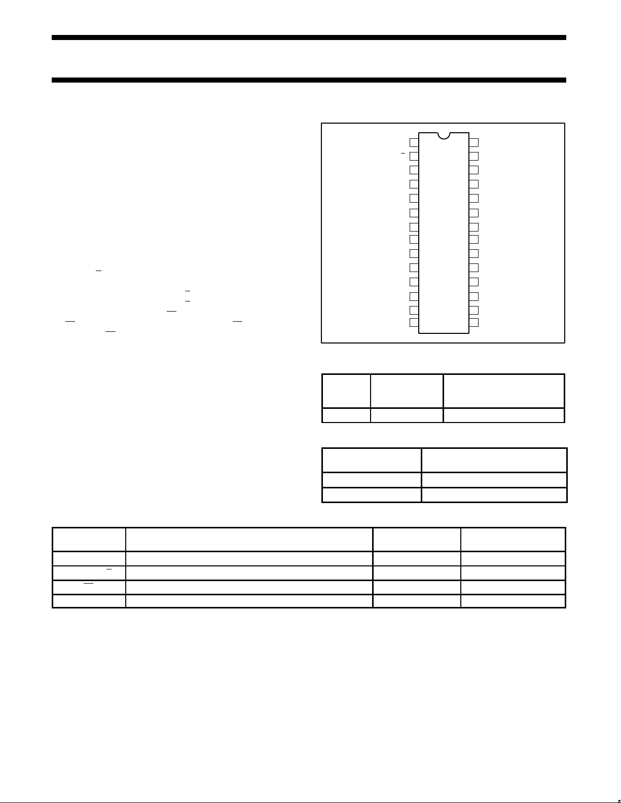
PIN CONFIGURA TION
1
LE
A0
B0
A1
B1
A2
A3
B3
Q3
Q2
Q1
2
3
4
5
6
9
10
11
12
SELECT A/B
TYPICAL
TYPE
PROPAGATION
DELAY
74F604 7.5ns 75mA
28
V
27
A4
26
B4
25
A5
24
B5
23
A6
227
B6
218B2 A7
20
B7
19
Q7
18
Q6
17
Q5
1613
Q4
1514GND Q0
TYPICAL SUPPLY CURRENT
CC
SF01115
(TOTAL)
ORDERING INFORMATION
DESCRIPTION
28-pin plastic DIP N74F604N
28-pin plastic SOL N74F604D
COMMERCIAL RANGE
= 5V ±10%, T
V
CC
= 0°C to +70°C
amb
INPUT AND OUTPUT LOADING AND FAN-OUT TABLE
PINS DESCRIPTION
74F (U.L.)
HIGH/LOW
A0–A7, B0–B7 Data inputs 1.0/0.033 20µA/20µA
SELECT A/B Select input 1.0/0.033 20µA/20µA
LE Latch Enable input (active Low) 1.0/0.033 20µA/20µA
Q0–Q7 Data outputs 150/40 3mA/24mA
NOTE:
One (1.0) FAST unit load is defined as: 20µA in the High state and 0.6mA in the Low state.
LOAD VALUE
HIGH/LOW
1990 Mar 01 853–0029 98991
1
Page 2
Philips Semiconductors Product specification
74F604Dual octal latch (3-State)
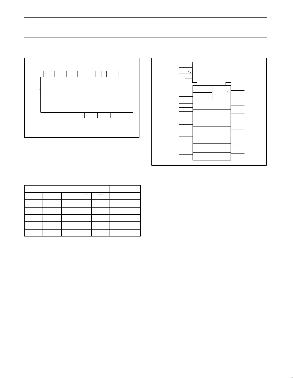
LOGIC SYMBOL
3
456
B0 B1 B2 B3 B4 B5 B6 B7
A0 A1 A2 A3
LE
1
SELECT A/B
2
VCC= Pin 28
GND = Pin 14
8910
Q0 Q1 Q2 Q3
15
13 12 11
27 26 25 24 23
A4 A5 A67A7
Q4 Q5 Q616Q7
17 18 19
22 21 20
FUNCTION TABLE
INPUTS OUTPUTS
A0–A7 B0–B7 SELECT A/B LE Q0–Q7
A data B data L ↑ B data
A data B data H ↑ B data
X X X L Z
X X L H B latched data
X X H H A latched data
H = High voltage level
L = Low voltage level
X = Don’t care
Z = High impedance “off” state
↑ = Low-to-High clock transition
SF01116
IEC/IEEE SYMBOL (IEEE/IEC)
2
1
3
4
5
6
7
8
9
10
27
26
25
24
23
22
21
20
G2
E1
EN
1D 2
1D 2
≥1
15
13
12
11
16
17
18
19
SF01117
1990 Mar 01
2
Page 3
Philips Semiconductors Product specification
74F604Dual octal latch (3-State)
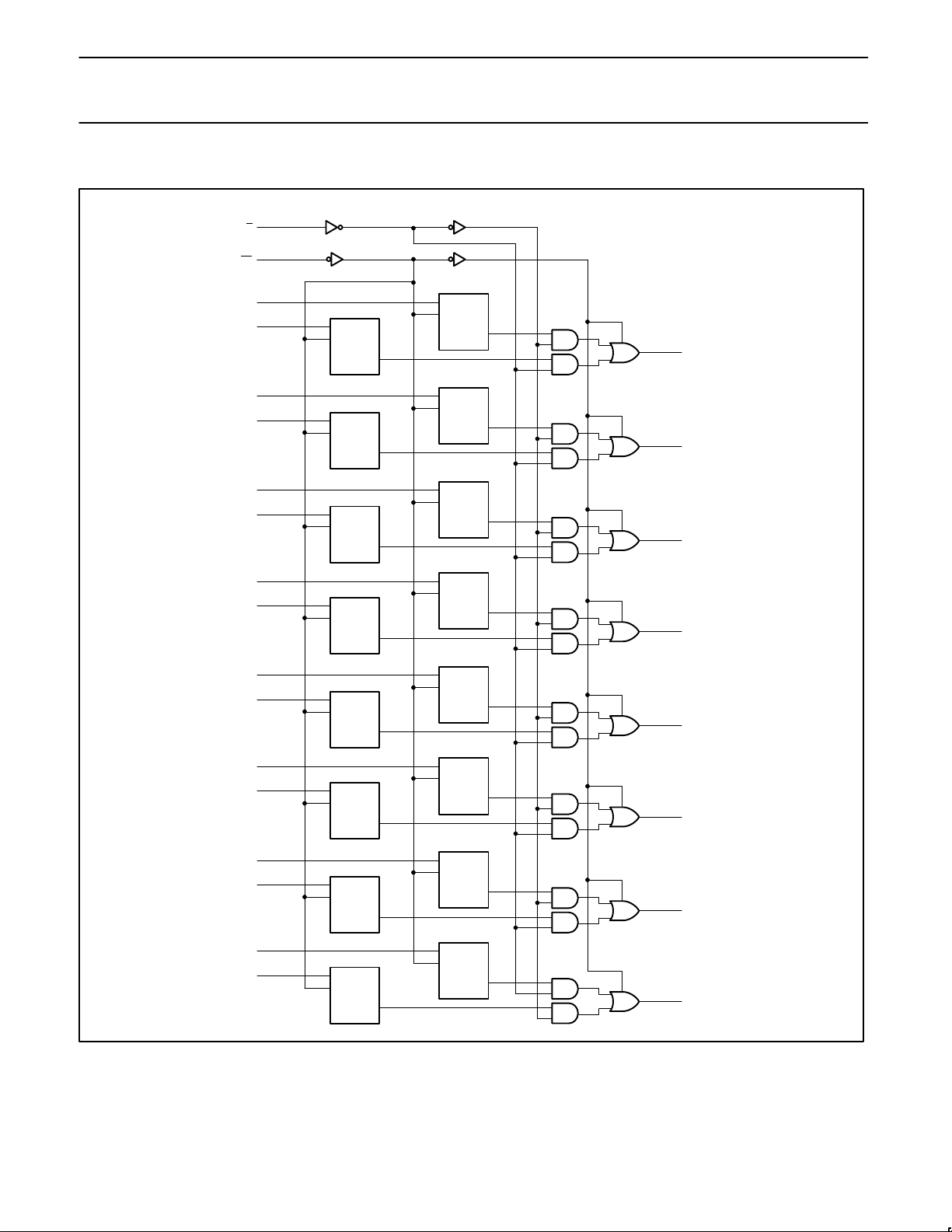
LOGIC DIAGRAM
SELECT A/B
2
1
LE
3
A0
4
B0
5
A1
6
B1
7
A2
8
B2
9
A3
10
B3
27
A4
26
B4
D
E
D
E
D
E
D
E
D
E
D
E
15
Q0
D
E
13
Q1
D
E
12
Q2
D
E
11
Q3
D
E
16
Q4
VCC = Pin 28
GND = Pin 14
1990 Mar 01
25
A5
24
B5
23
A6
22
B6
21
A7
20
B7
D
E
D
E
D
E
D
E
17
Q5
D
E
18
Q6
D
E
19
Q7
SF01118
3
Page 4
Philips Semiconductors Product specification
SYMBOL
PARAMETER
UNIT
74F604Dual octal latch (3-State)
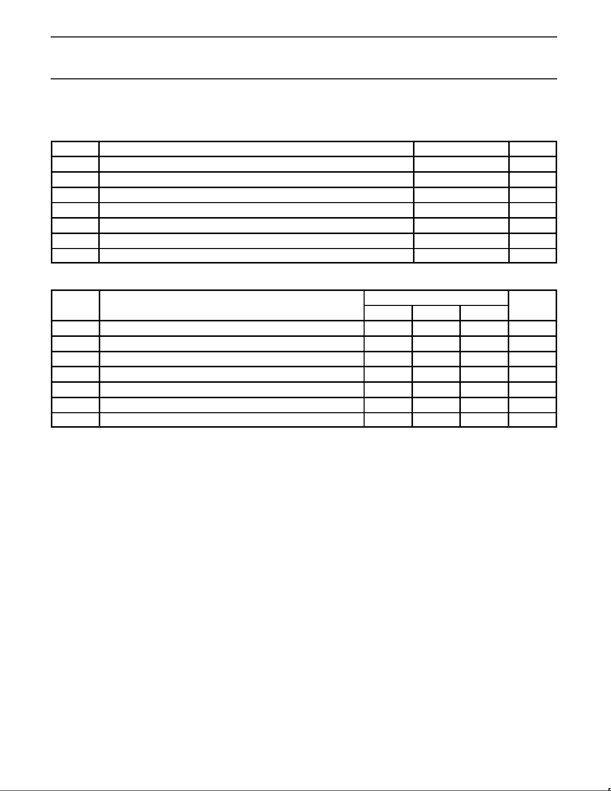
ABSOLUTE MAXIMUM RATINGS
(Operation beyond the limits set forth in this table may impair the useful life of the device.
Unless otherwise noted these limits are over the operating free-air temperature range.)
SYMBOL
V
V
I
IN
V
I
OUT
T
T
CC
IN
OUT
amb
stg
Supply voltage –0.5 to +7.0 V
Input voltage –0.5 to +7.0 V
Input current –30 to +5 mA
Voltage applied to output in High output state –0.5 to +V
Current applied to output in Low output state 48 mA
Operating free-air temperature range 0 to +70 °C
Storage temperature range –65 to +150 °C
RECOMMENDED OPERATING CONDITIONS
V
V
V
I
I
I
T
CC
IH
IL
IK
OH
OL
amb
Supply voltage 4.5 5.0 5.5 V
High-level input voltage 2.0 V
Low-level input voltage 0.8 V
Input clamp current –18 mA
High-level output current –3 mA
Low-level output current 24 mA
Operating free-air temperature range 0 70 °C
PARAMETER RATING UNIT
CC
V
LIMITS
MIN NOM MAX
1990 Mar 01
4
Page 5
Philips Semiconductors Product specification
SYMBOL
PARAMETER
TEST CONDITIONS
1
UNIT
VOHHigh-l
VCC MIN, VIL MAX,
VOLL
VCC MIN, VIL MAX,
ICCSupply current (total)
V
CC
MAX
74F604Dual octal latch (3-State)
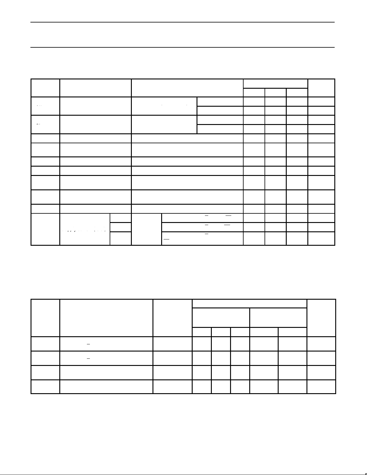
DC ELECTRICAL CHARACTERISTICS
(Over recommended operating free-air temperature range unless otherwise noted.)
1
MIN TYP
±10%V
±5%V
±10%V
±5%V
CC
CC
CC
CC
V
I
I
I
IH
I
IL
I
OZH
I
OZL
I
OS
I
evel output voltage
ow-level output voltage
IK
Input clamp voltage VCC = MIN, II = I
Input current at maximum input
voltage
VCC = MIN, VIL = MAX,
V
IH
= MIN, I
OH
= MAX
VCC = MIN, VIL = MAX,
VIH = MIN, I
OL
IK
= MAX
VCC = 0.0V, VI = 7.0V 100 µA
High-level input current VCC = MAX, VI = 2.7V 20 µA
Low-level input current VCC = MAX, VI = 0.5V –20 µA
Off state output current,
High-level voltage applied
Off state output current,
Low-level voltage applied
Short-circuit output current
Supply current (total)
I
I
I
VCC = MAX, VO = 2.7V 50 µA
VCC = MAX, V
3
VCC = MAX –60 –150 mA
CCH
CCL
V
= MAX
=
CCZ
= 0.5V –50 µA
O
An, Bn, SELECT A/B = 4.5V, LE = ↑ 60 82 mA
An, Bn, SELECT A/B=GND, LE = ↑ 75 100 mA
An, Bn, SELECT A/B = GND,
= GND
LE
NOTES:
1. For conditions shown as MIN or MAX, use the appropriate value specified under recommended operating conditions for the applicable type.
2. All typical values are at V
3. Not more than one output should be shorted at a time. For testing I
CC
= 5V, T
techniques are preferable in order to minimize internal heating and more accurately reflect operational values. Otherwise, prolonged shorting
amb
= 25°C.
, the use of high-speed test apparatus and/or sample-and-hold
OS
of a High output may raise the chip temperature well above normal and thereby cause invalid readings in other parameter tests. In any
sequence of parameter tests, I
tests should be performed last.
OS
LIMITS
2
MAX
2.4 V
2.7 3.4 V
0.35 0.50 V
0.35 0.50 V
–0.73 –1.2 V
75 100 mA
AC ELECTRICAL CHARACTERISTICS
SYMBOL PARAMETER
t
PLH
t
PHL
t
PLH
t
PHL
t
PZH
t
PZL
t
PHZ
t
PLZ
1990 Mar 01
Propagation delay
SELECT A/B
to Qn (B latch)
Propagation delay
SELECT A/B
to Qn (A latch)
Output Enable time
to High or Low level
Output Disable time
from High or Low level
TEST
CONDITION
Waveform 1
Waveform 2
Waveform 4
Waveform 5
Waveform 4
Waveform 5
LIMITS
VCC = +5V
= +25°C
T
amb
= 50pF, RL = 500Ω
C
L
VCC = +5V ± 10%
T
amb
= 50pF, RL = 500Ω
C
L
MIN TYP MAX MIN MAX
5.0
6.0
6.0
4.0
5.0
5.0
5.0
5.0
7.0
8.5
8.0
6.5
7.5
7.5
7.0
7.0
9.0
10.5
10.0
8.5
9.5
9.5
9.5
9.5
4.5
5.5
5.5
3.5
4.5
4.5
4.5
4.5
5
= 0°C to +70°C
10.0
11.5
11.5
9.0
10.5
11.0
11.0
11.0
UNIT
ns
ns
ns
ns
Page 6
Philips Semiconductors Product specification
74F604Dual octal latch (3-State)
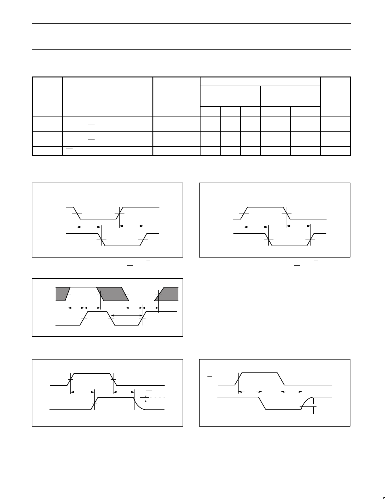
AC SETUP REQUIREMENTS
LIMITS
SYMBOL PARAMETER
TEST
CONDITION
VCC = +5V
= +25°C
T
amb
= 50pF, RL = 500Ω
C
L
MIN TYP MAX MIN MAX
ts(H)
(L)
t
s
th(H)
(L)
t
h
Setup time, High or Low
An, Bn to LE
Hold time, High or Low
An, Bn to LE
Waveform 3
Waveform 3
1.0
2.0
0
1.0
tW(L) LE Pulse width, Low Waveform 3 5.0 6.0 ns
AC WAVEFORMS
For all waveforms, VM = 1.5V.
The shaded areas indicate when the input is permitted to change for predictable output performance.
VCC = +5V ± 10%
= 0°C to +70°C
T
amb
= 50pF, RL = 500Ω
C
L
2.0
3.0
0
1.5
UNIT
ns
ns
SELECT A/B
Qn
V
M
t
PHL
V
M
t
PLH
V
M
V
M
SF01119
Waveform 1. Propagation Delay, SELECT A/B To Output
tw(L)
=H)
V
V
M
M
V
M
SF01121
An, Bn
(B latched data=Low. LE
V
V
M
M
ts(H) ts(L) th(L)th(H)
LE
V
M
V
M
Waveform 3. Data Setup and Hold Times,
Latch Enable Pulse Width
LE
Qn
V
M
t
PZH
V
M
t
PHZ
V
M
VOH -0.3V
0V
SF01122
Waveform 4. 3-State Output Enable Time to High Level and
Output Disable Time from High Level
SELECT A/B
Qn
V
M
t
PHL
V
M
t
PLH
V
M
V
M
SF01120
Waveform 2. Propagation Delay, SELECT A/B to Output
=H)
V
M
t
PLZ
V
+0.3V
OL
SF01123
LE
Qn
(A latched data=Low. LE
V
M
t
PZL
V
M
Waveform 5. 3-State Output Enable Time to Low Level and
Output Disable Time from Low Level
1990 Mar 01
6
Page 7
Philips Semiconductors Product specification
74F604Dual octal latch (3-State)
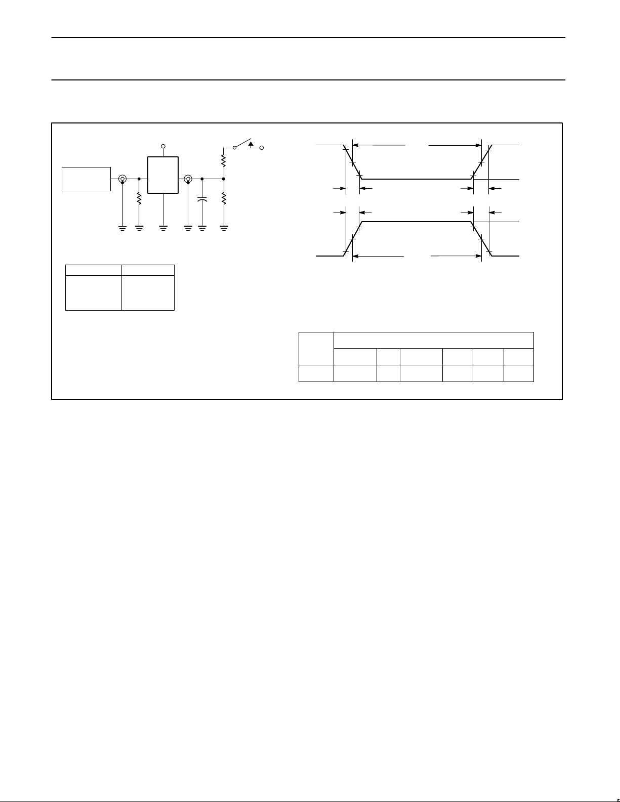
TEST CIRCUIT AND WAVEFORMS
V
V
PULSE
GENERATOR
IN
R
Test Circuit for 3-State Outputs
SWITCH POSITION
TEST SWITCH
t
t
PLZ
PZL
closed
closed
All other open
T
D.U.T.
CC
V
OUT
7.0V
R
L
R
C
L
L
NEGATIVE
PULSE
POSITIVE
PULSE
90%
10%
V
M
10%
t
THL (tf
t
TLH (tr
90%
V
M
Input Pulse Definition
t
w
V
M
10%
)
)
t
w
t
TLH (tr
t
THL (tf
)
)
90%
V
M
90%
10%
AMP (V)
0V
AMP (V)
0V
DEFINITIONS:
= Load resistor;
R
L
see AC electrical characteristics for value.
= Load capacitance includes jig and probe capacitance;
C
L
see AC electrical characteristics for value.
= Termination resistance should be equal to Z
R
T
pulse generators.
OUT
of
family
74F
INPUT PULSE REQUIREMENTS
V
amplitude
3.0V
M
1.5V
rep. rate
1MHz 500ns
t
w
t
TLHtTHL
2.5ns 2.5ns
SF00777
1990 Mar 01
7
 Loading...