

Datasheet 74F543SPC, 74F543SCX, 74F543SC, 74F543PC, 74F543MSAX Datasheet (Fairchild Semiconductor)
...Page 1
April 1988
Revised March 1999
74F543 Octal Registered Transceiver
© 1999 Fairchild Semiconductor Corporation DS009554.prf www.fairchildsemi.com
74F543
Octal Registered Transceiver
General Description
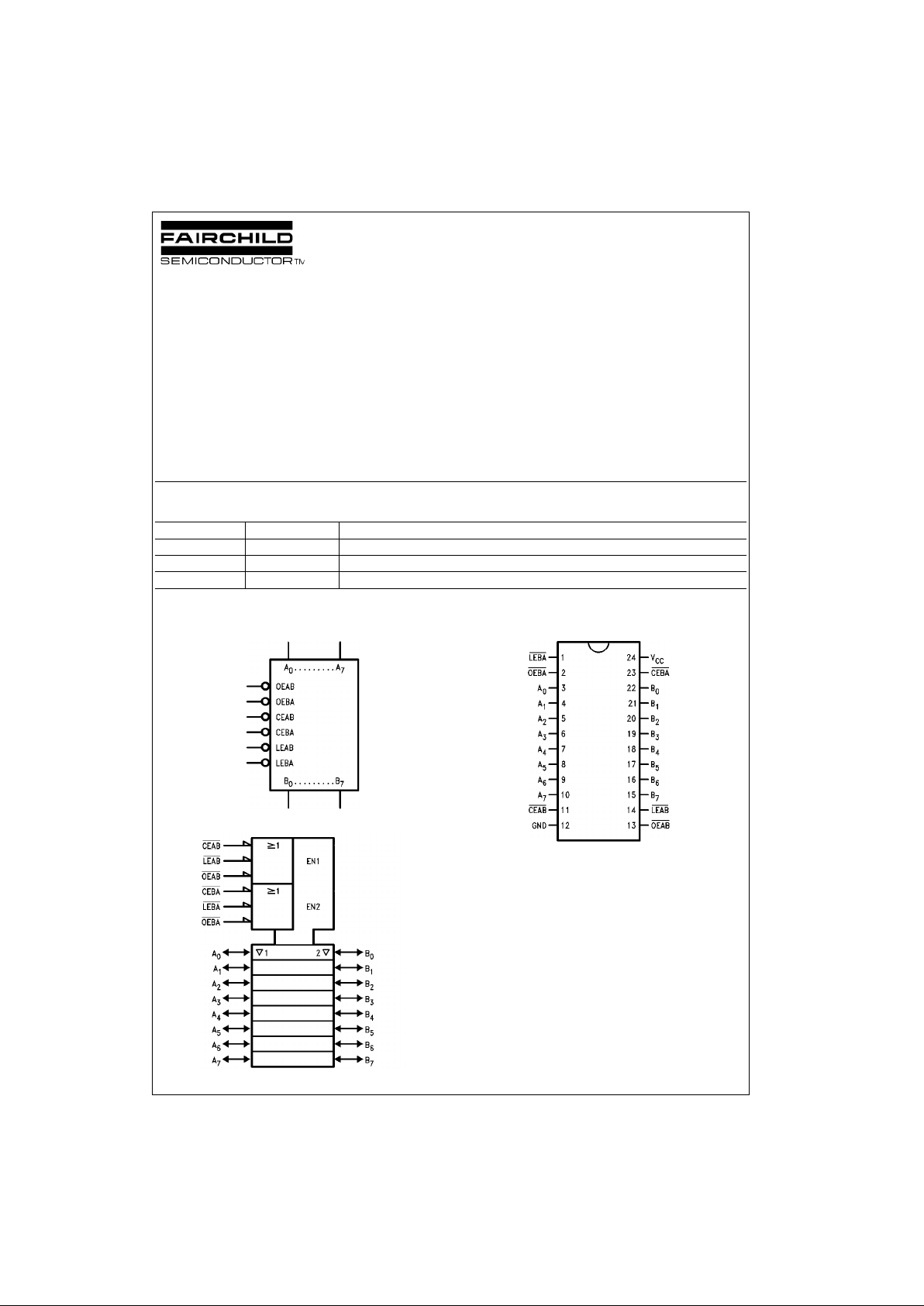
The F543 octal transceiver contains two sets of D-type
latches for temporary storage of data flowing in either
direction. Separate Latch Enable and Output Enable inputs
are provided for each reg ister to permit indep endent control of inputting and outputt ing in either direction of data
flow. The A outputs are guaranteed to sink 24 mA while the
B outputs are rated for 64 mA.
Features
■ 8-bit octal transceiver
■ Back-to-back registers for storage
■ Separate controls for data flow in each direction
■ A outputs sink 24 mA
■ B outputs sink 64 mA
Ordering Code:
Devices also availab le in Tape and Reel. Specify by appending th e s uffix let t er “X” to the ordering cod e.
Logic Symbols
IEEE/IEC
Connection Diagram
Order Number Package Number Package Description
74F543SC M24B 24-Lead Small Outline Integrated Circuit (SOIC), JEDEC MS-013, 0.300 Wide
74F543MSA MSA24 24-Lead Shrink Small Outline Package (SSOP), EIAJ TYPE II, 5.3mm Wide
74F543SPC N24C 24-Lead Plastic Dual-In-Line Package (PDIP), JEDEC MS-100, 0.300 Wide
Page 2
www.fairchildsemi.com 2
74F543
Unit Loading/Fan Out
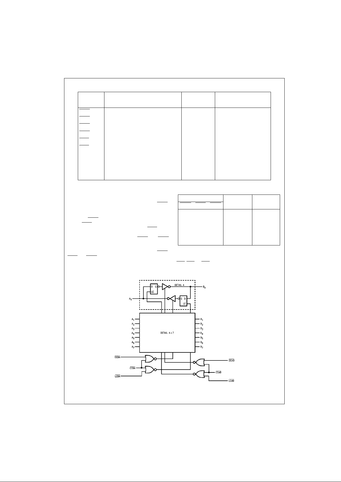
Functional Description
The F543 contains tw o sets of eight D-type latches, with
separate input and outpu t controls for each set. For data
flow from A to B, for example, the A-to-B Enable (CEAB
)
input must be LOW in order to e nter data from A
0–A7
or
take data from B
0–B7
, as indicated in the Data I/O Contr ol
Table. With CEAB
LOW, a LOW signal on the A-to-B Lat ch
Enable (LEAB
) input makes the A-to-B latches transparent;
a subsequent LOW-to-HIG H transition of the LEAB
signal
puts the A latches in the storage mode and their outputs no
longer change wit h the A inputs. With CEAB
and OEAB
both LOW, the 3-STATE B outp ut buffers are active and
reflect the data present at the output of the A latches. Control of data flow from B to A is similar, but using the CEBA
,
LEBA
and OEBA inputs.
Data I/O Control Table
H = HIGH Voltage Level
L = LOW Voltage Level
X = Immaterial
A-to-B data flow shown ; B-to-A f low control is the same, except using
CEBA, LEBA and OEBA
Logic Diagram
Please note that this diagram is provided o nly f or t he understanding of lo gic operations and should not be used to estimate propagation delays.
Pin Names Description
U.L. Input I
IH/IIL
HIGH/LOW Output IOH/I
OL
OEAB A-to-B Output Enable Input (Active LOW) 1.0/1.0 20 µA/−0.6 mA
OEBA
B-to-A Output Enable Input (Active LOW) 1.0/1.0 20 µA/−0.6 mA
CEAB
A-to-B Enable Input (Active LOW) 1.0/2.0 20 µA/−1.2 mA
CEBA
B-to-A Enable Input (Active LOW) 1.0/2.0 20 µA/−1.2 mA
LEAB
A-to-B Latch Enable Input (Active LOW) 1.0/1.0 20 µA/−0.6 mA
LEBA
B-to-A Latch Enable Input (Active LOW) 1.0/1.0 20 µA/−0.6 mA
A
0–A7
A-to-B Data Inputs or 3.5/1.083 70 µA/−650 µA
B-to-A 3-STATE Outputs 150/40 (33.8) −3 mA/24 mA (20 mA)
B
0–B7
B-to-A Data Inputs or 3.5/1.083 70 µA/−650 µA
A-to-B 3-STATE Outputs 600/106.6 (80) −12 mA /64 mA (48 mA)
Inputs
Latch
Status
Output
Buffers
CEAB
LEAB OEAB
H X X Latched High Z
X H X Latched —
L L X Transparent —
X X H — High Z
L X L — Driving
Page 3
3 www.fairchildsemi.com
74F543
Absolute Maximum Ratings(Note 1) Recommended Operating
Conditions
Note 1: Absolute maximum ratings are values beyon d which the device
may be damaged or have its useful life impaired . Functional operation
under these condit ions is not implied.
Note 2: Either voltage limit or curren t limit is sufficient to protect in puts.
DC Electrical Characteristics
Storage Temperature −65°C to +150°C
Ambient Temperature under Bias −55°C to +125°C
Junction Temperature under Bias −55°C to +150°C
V
CC
Pin Potential to Ground Pin −0.5V to +7.0V
Input Voltage (Note 2) −0.5V to +7.0V
Input Current (Note 2) −30 mA to +5.0 mA
Voltage Applied to Output
in HIGH State (with V
CC
= 0V)
Standard Output −0.5V to V
CC
3-STATE Output −0.5V to +5.5V
Current Applied to Output
in LOW State (Max) twice the rated I
OL
(mA)
Free Air Ambi ent Temperature 0°C to +70°C
Supply Voltage +4.5V to +5.5V
Symbol Parameter Min Typ Max Units
V
CC
Conditions
V
IH
Input HIGH Voltage 2.0 V Recognized as a HIGH Signal
V
IL
Input LOW Voltage 0.8 V Recognized as a LOW Signal
V
CD
Input Clamp Diode Voltage −1.2 V Min IIN = −18 mA
V
OH
Output HIGH Voltage 10% V
CC
2.5 IOH = −1 mA (An)
10% V
CC
2.4 IOH = −3 mA (An, Bn)
5% V
CC
2.7 V Min IOH = −1 mA (An)
5% V
CC
2.7 IOH = −3 mA (An, Bn)
10% V
CC
2.0 IOH = −15 mA (Bn)
V
OL
Output LOW 10% V
CC
0.5 V Min IOL = 24 mA (An)
Voltage 10% V
CC
0.55 IOL = 64 mA (Bn)
I
IH
Input HIGH Current 5.0 µAMaxVIN = 2.7V
I
BVI
Input HIGH Current
7.0 µAMax
(OEAB, OEBA, L EAB,
Breakdown Test
LEBA, CEAB, CEBA)
I
BVIT
Input HIGH Current 0.5 mA Max VIN = 5.5V (An, Bn)
Breakdown (I/O)
I
CEX
Output HIGH 50 µAMaxV
OUT
= V
CC
Leakage Current
V
ID
Input Leakage 4.75 V 0.0 IID = 1.9 µA
Test All Other Pins Grounded
I
OD
Output Leakage 3.75 µA0.0V
IOD
= 150 mV
Circuit Current All Other Pins Grounded
I
IL
Input LOW Current −0.6
mA Max
VIN = 0.5V (OEAB, OEBA)
−1.2
VIN = 0.5V (CEAB, CEBA)
IIH + I
OZH
Output Leakage Current 70 µAMaxV
OUT
= 2.7V (An, Bn)
IIL + I
OZL
Output Leakage Current −650 µAMaxV
OUT
= 0.5V (An, Bn)
I
OS
Output Short-Circuit Current −60 −150 mA Max V
OUT
= 0V (An)
−100 −225 V
OUT
= 0V (Bn)
I
ZZ
Bus Drainage Test 500 µA0.0VV
OUT
= 5.25V (An, Bn)
I
CCH
Power Supply Current 67 100 mA Max VO = HIGH
I
CCL
Power Supply Current 83 125 mA Max VO = LOW
I
CCZ
Power Supply Current 83 125 mA Max VO = HIGH Z
Page 4

www.fairchildsemi.com 4
74F543
AC Electrical Characteristics
AC Operating Requirements
Symbol Parameter
TA = +25°C
Units
VCC = +5.0V TA = 0°C to +70°C
CL = 50 pF CL = 50 pF
Min Typ Max Min Max
t
PLH
Propagation Delay 3.0 5.5 7.5 3.0 8.5
t
PHL
Transparent Mode 3.0 5.0 6.5 3.0 7.5 ns
An to Bn or Bn to A
n
t
PLH
Propagation Delay 4.5 8.5 11.0 4.5 12.5 ns
t
PHL
LEBA to A
n
4.5 8.5 11.0 4.5 12.5
t
PLH
Propagation Delay 4.5 8.5 11.0 4.5 12.5 ns
t
PHL
LEAB to B
n
4.5 8.5 11.0 4.5 12.5
t
PZH
Output Enable Time
t
PZL
OEBA or OEAB to An or B
n
3.0 7.0 9.0 3.0 10.0
CEBA or CEAB to An or B
n
4.0 7.5 10.5 4.0 12.0
ns
t
PHZ
Output Disable Time
t
PLZ
OEBA or OEAB to An or B
n
1.0 6.0 8.0 1.0 9.0
CEBA or CEAB to An or B
n
2.5 5.5 10.5 2.5 11.5
Symbol Parameter
TA = +25°C
UnitsVCC = +5.0V TA = 0°C to +70°C
Min Max Min Max
tS(H) Setup Time, HIGH or LOW 3.0 3.5
tS(L)
An or Bn to LEBA or LEAB
3.0 3.5
ns
tH(H) Hold Time, HIGH or LOW 3.0 3.5
tH(L)
An or Bn to LEBA or LEAB
3.0 3.5
tW(L) Latch Enable, B to A or 8.0 9.0 ns
B to A Pulse Width, LOW
Page 5

5 www.fairchildsemi.com
74F543
Physical Dimensions inches (millimeters) unless otherwise noted
24-Lead Small Outline Integrated Circuit (SOIC), JEDEC MS-013, 0.300 Wide
Package Number M24B
24-Lead Shrink Small Outline Package (SSOP), EIAJ TYPE II, 5.3mm Wide
Package Number MSA24
Page 6

www.fairchildsemi.com 6
74F543
Physical Dimensions inches (millimeters) unless otherwise noted (Continued)
24-Lead Plastic Dual-In-Line Package (PDIP), JEDEC MS-010, 0.600 Wide
Package Number N24A
Page 7

Fairchild does not assume any responsibility for use of any circuitry described, no circuit patent licenses are implied and Fairchild reserves the right at any time without notice to change said circuitry and specifications.
74F543 Octal Registered Transceiver
LIFE SUPPORT POLICY
FAIRCHILD’S PRODUCTS ARE NOT AUTHORIZED FOR USE AS CRITICAL COMPONENTS IN LIFE SUPPORT
DEVICES OR SYSTEMS WITHOUT THE EXPRESS WRITTEN APPROVAL OF THE PRESIDENT OF FAIRCHILD
SEMICONDUCTOR CORPORATION. As used herein:
1. Life support devices or systems are dev ic es or syste ms
which, (a) are intended for surgical implant into the
body, or (b) support or sustain life, and (c) whose failure
to perform when properly used in accordance with
instructions for use provided i n the labe li ng, can be re asonably expected to result in a significant injury to the
user.
2. A critical componen t in any com ponent o f a l ife supp ort
device or system whose failu re to perform can b e reasonably expected to c ause th e fa i lure of the li fe s upp or t
device or system, or to affect its safety or effectiveness.
www.fairchildsemi.com
Physical Dimensions inches (millimeters) unless otherwise noted (Continued)
24-Lead Plastic Dual-In-Line Package (PDIP), JEDEC MS-100, 0.300 Wide
Package Number N24C
 Loading...