

Page 1
Philips Semiconductors Product specification
74F539Dual 1-of-4 decoder (3-State)
DESCRIPTION
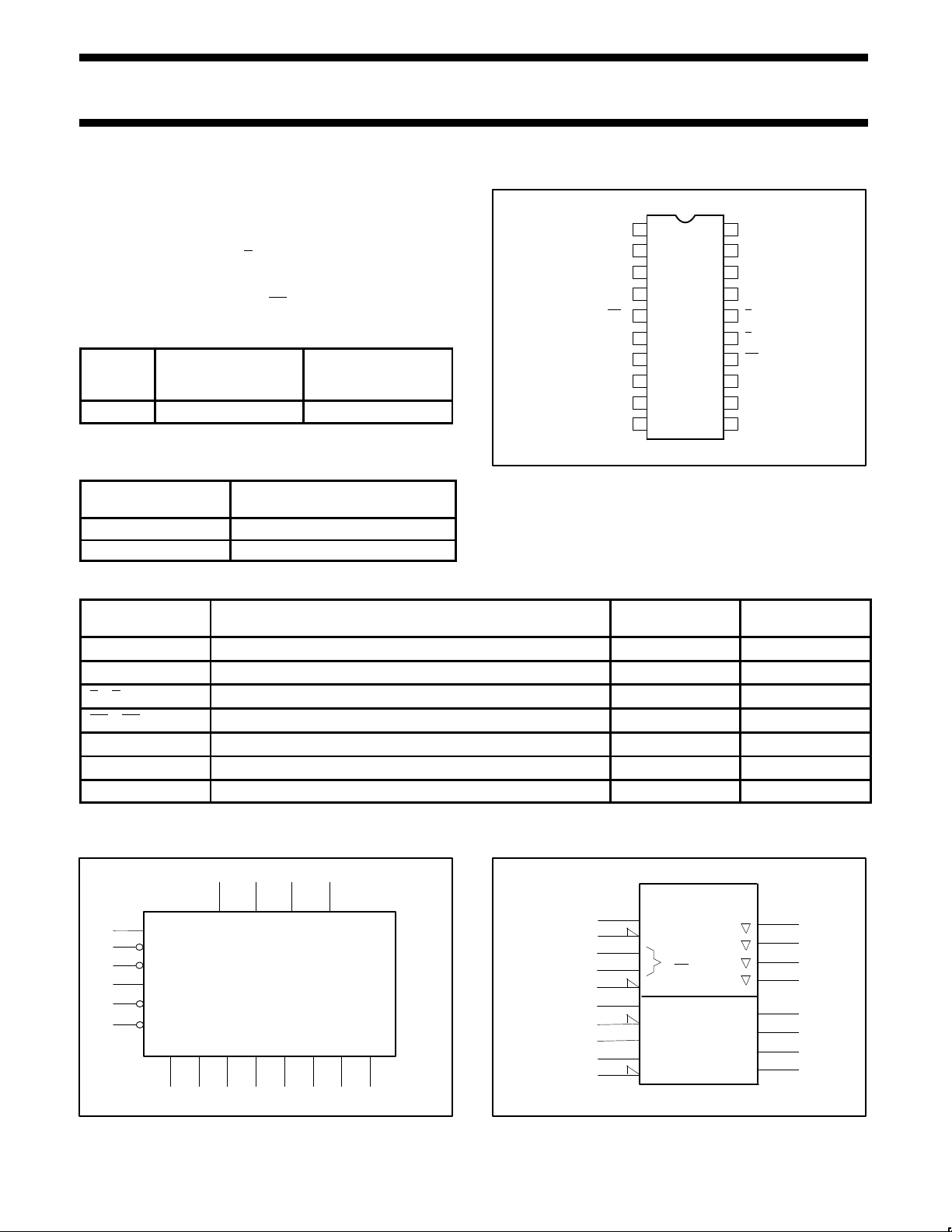
PIN CONFIGURA TION
The 74F539 contains two independent decoders. Each accepts two
address (A0 - A1) input signals and decodes them to select one of
four mutually exclusive outputs. A Polarity control (P) input
determines whether the outputs are active Low (P=H) or active High
(P=L). An active-Low Enable (E
) is available for data demultiplexing.
Data is routed to the selected output in non-inverted or inverted form
in the active-Low mode or inverted form in the active-High mode. A
High signal on the Output Enable (OE
n) input forces the 3-State
outputs to the high impedance state.
TYPE
TYPICAL
PROPAGATION DELAY
TYPICAL SUPPL Y
CURRENT
(TOTAL)
74F539 7.5ns 40mA
Q2b
1
Q1b
2
Q0b
3
Pb
4
OEb
5
A0a
6
A1a
7
Q3a
8
Q2a
9
10 11
GND
V
20
CC
Q3b
19
A1b
18
A0b
17
E
b
16
Ea
15
OE
a
14
Pa
13
12
Q0a
Q1a
ORDERING INFORMATION
DESCRIPTION COMMERCIAL RANGE
20-Pin Plastic DIP N74F539N
20-Pin Plastic SOL N74F539D
= 5V ±10%, T
V
CC
= 0°C to +70°C
amb
INPUT AND OUTPUT LOADING AND FAN-OUT TABLE
PINS DESCRIPTION
74F(U.L.)
HIGH/LOW
A0a - A1a Decoder A Address inputs 1.0/1.0 20µA/0.6mA
A0b - A1b Decoder B Address inputs 1.0/1.0 20µA/0.6mA
Ea, Eb Enable inputs (active Low) 1.0/1.0 20µA/0.6mA
OEa, OEb Output Enable inputs (active Low) 1.0/1.0 20µA/0.6mA
Pa, Pb Polarity control inputs 1.0/1.0 20µA/0.6mA
Q0a–Q3a Decoder A Data outputs 150/40 3.0mA/24mA
Q0b–Q3b Decoder A Data outputs 150/40 3.0mA/24mA
NOTE: One (1.0) FAST Unit Load is defined as: 20µA in the High state and 0.6mA in the Low state.
LOAD VALUE
HIGH/LOW
SF01013
LOGIC SYMBOL
6717
13
15
14
4
16
5
VCC = Pin 20
GND = Pin 10
Pa
Ea
OEa
Pb
Eb
OEb
Q0a Q1a Q2a Q3a Q0b Q1b Q2b Q3b
A0a A1a A0b
12 11 9 8 3 2 1 19
1990 Feb 23 853–1274 98905
18
A1b
SF01014
LOGIC SYMBOL (IEEE/IEC)
4
5
17
18
16
13
14
6
7
15
1
DMUX
N4
EN
0
G
1
0,4
1,4
0
2,4
3
3,4
3
2
1
19
12
11
9
8
SF01015
Page 2
Philips Semiconductors Product specification
OPERATING MODE
74F539Dual 1-of-4 decoder (3-State)
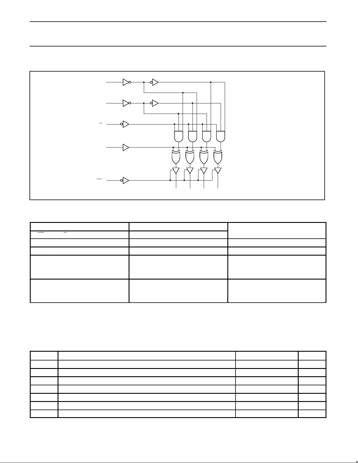
LOGIC DIAGRAM
7, 18
A1n
6, 17
A0n
15, 16
En
13, 4
Pn
14, 5
V
= Pin 20
CC
GND = Pin 10
OEn
12, 3 11, 2 9, 1 8, 19
Q0n Q1n Q2n Q3n
SF01016
FUNCTION TABLE
INPUTS OUTPUTS
OE
n
En A1n A0n Q0n Q1n Q2n Q3n
H X X X Z Z Z Z High Impedance
L H X X Qn=P Disable
L
L
L
L
L
L
L
L
L
L
L
L
L
L
L
L
L
L
H
H
L
L
H
H
L
H
L
H
L
H
L
H
H
L
L
L
L
H
H
H
L
H
L
L
H
L
H
H
L
L
H
L
H
H
L
H
L
L
Active High output
L
H
H
H
Active Low output
H
L
H = High voltage level
L = Low voltage level
X = Don’t care
Z = High impedance “off” state
ABSOLUTE MAXIMUM RATINGS
(Operation beyond the limits set forth in this table may impair the useful life of the device.
Unless otherwise noted these limits are over the operating free-air temperature range.)
SYMBOL
V
CC
V
IN
I
IN
V
OUT
I
OUT
T
amb
T
stg
Supply voltage –0.5 to +7.0 V
Input voltage –0.5 to +7.0 V
Input current –30 to +5 mA
Voltage applied to output in High output state –0.5 to +V
Current applied to output in Low output state 48 mA
Operating free-air temperature range 0 to +70 °C
Storage temperature –65 to +150 °C
PARAMETER RATING UNIT
(P = L)
(P = H)
CC
V
1990 Feb 23
2
Page 3
Philips Semiconductors Product specification
SYMBOL
PARAMETER
UNIT
SYMBOL
PARAMETER
TEST CONDITIONS
1
UNIT
V
CC
MIN, V
IL
MAX
VOLL
V
CC
MIN, V
IL
MAX
74F539Dual 1-of-4 decoder (3-State)
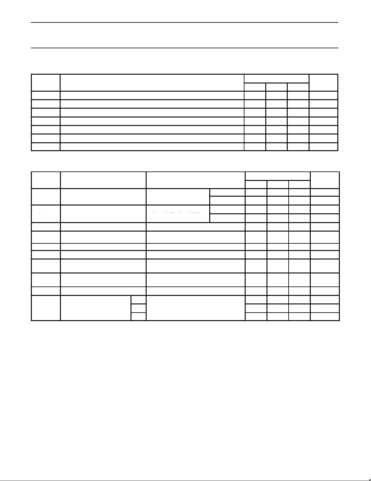
RECOMMENDED OPERATING CONDITIONS
LIMITS
MIN NOM MAX
V
CC
V
IH
V
IL
I
IK
I
OH
I
OL
T
amb
DC ELECTRICAL CHARACTERISTICS
(Over recommended operating free-air temperature range unless otherwise noted.)
V
OH
V
IK
I
I
I
IH
I
IL
I
OZH
I
OZL
I
OS
I
CC
NOTES:
1. For conditions shown as MIN or MAX, use the appropriate value under the recommended operating conditions for the applicable type.
2. All typical values are at V
3. Not more than one output should be shorted at a time. For testing I
techniques are preferable in order to minimize internal heating and more accurately reflect operational values. Otherwise, prolonged shorting
of a High output may raise the chip temperature well above normal and thereby cause invalid readings in other parameter tests. In any
sequence of parameter tests, I
Supply voltage 4.5 5.0 5.5 V
High-level input voltage 2.0 V
Low-level input voltage 0.8 V
Input clamp current –18 mA
High-level output current –3 mA
Low-level output current 24 mA
Operating free-air temperature range 0 70 °C
LIMITS
2
MAX
2.4 V
2.7 3.4 V
0.35 0.50 V
0.35 0.50 V
–0.73 –1.2 V
High-level output voltage
ow-level output voltage
=
= MIN, I
V
IH
V
= MIN, VIL = MAX,
=
= MIN, IOL = MAX
V
IH
OH
=
= MAX
=
,
,
V
= MIN, VIL = MAX,
Input clamp voltage VCC = MIN, II = I
Input current at maximum input
voltage
VCC = MAX, VI = 7.0V 100 µA
1
±10%V
±10%V
IK
±5%V
±5%V
MIN TYP
CC
CC
CC
CC
High-level input current VCC = MAX, VI = 2.7V 20 µA
Low-level input current VCC = MAX, VI = 0.5V –0.6 mA
Off-state output current
High-level voltage applied
Off-state output current
Low-level voltage applied
Short-circuit output current
3
Supply current I
= 5V, T
CC
OS
= 25°C.
amb
should be performed last.
I
CCH
CCL
I
CCZ
VCC = MAX, VO = 2.7V 50 µA
V
= MAX, VO = 0.5V –50 µA
CC
VCC = MAX –60 –150 mA
35 50 mA
VCC = MAX 40 55 mA
40 60 mA
, the use of high-speed test apparatus and/or sample-and-hold
OS
1990 Feb 23
3
Page 4
Philips Semiconductors Product specification
74F539Dual 1-of-4 decoder (3-State)
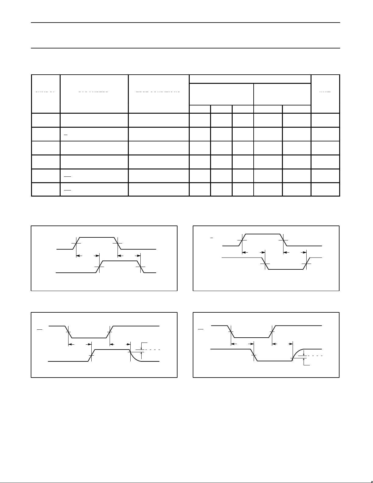
AC ELECTRICAL CHARACTERISTICS
LIMITS
T
SYMBOL PARAMETER TEST CONDITIONS
t
PLH
t
PHL
t
PLH
t
PHL
t
PLH
t
PHL
t
PLH
t
PHL
t
PZH
t
PZL
t
PHZ
t
PLZ
Propagation delay
An to Qn
Propagation delay
n to Qn
E
Propagation delay
Pn to Qn
Propagation delay
Pn to Qn (INV)
Output Enable time
n to Qn
OE
Output Disable time
n to Qn
OE
Waveform 1
Waveform 2
Waveform 1
Waveform 2
Waveform 3
Waveform 4
Waveform 3
Waveform 4
= +25°C T
amb
VCC = +5.0V VCC = +5.0V ± 10%
CL = 50pF, RL = 500Ω CL = 50pF, RL = 500Ω
MIN TYP MAX MIN MAX
4.5
3.0
5.0
3.0
4.0
3.5
6.0
4.0
2.5
5.5
1.5
2.0
8.5
8.0
7.5
7.0
6.5
5.5
11.5
6.0
4.0
7.0
3.0
4.0
12.5
12.5
11.0
11.0
9.5
9.0
14.5
9.0
7.5
10.5
6.0
8.0
= 0°C to +70°C
amb
4.0
3.0
4.5
3.0
3.5
3.0
5.0
4.0
2.0
5.0
1.0
1.5
13.5
13.0
12.0
11.5
10.5
9.5
15.5
9.5
8.5
11.5
6.5
8.5
UNIT
ns
ns
ns
ns
ns
ns
ns
ns
ns
ns
ns
ns
AC WAVEFORMS
For all waveforms, VM = 1.5V.
An, Pn
Qn
V
M
t
PLH
V
Waveform 1. Propagation Delay for
Non-Inverting Outputs
OEn
Qn
V
M
t
PZH
V
M
Waveform 3. 3-State Output Enable Time to High Level
and Output Disable Time from High Level
V
M
t
PHL
M
V
M
t
PHZ
V
M
SF01017
VOH -0.3V
0V
SF01019
En, Pn
Qn
V
M
t
PHL
V
M
t
PLH
V
M
V
M
Waveform 2. Propagation Delay for
Inverting Outputs
OEn
Qn
V
M
t
PZL
V
M
t
PLZ
V
M
Waveform 4. 3-State Output Enable Time to Low Level
and Output Disable Time from Low Level
SF01018
V
OL
SF01020
+0.3V
1990 Feb 23
4
Page 5
Philips Semiconductors Product specification
74F539Dual 1-of-4 decoder (3-State)
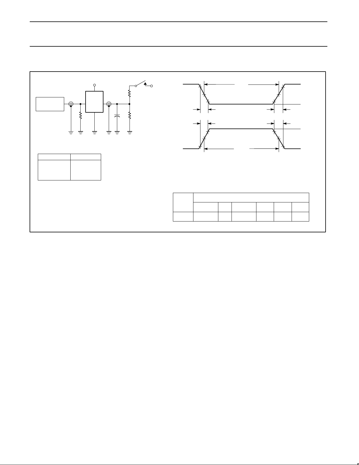
TEST CIRCUIT AND WAVEFORM
V
V
PULSE
GENERATOR
IN
R
Test Circuit for 3-State Outputs
SWITCH POSITION
TEST SWITCH
t
t
PLZ
PZL
closed
closed
All other open
T
D.U.T.
CC
V
OUT
7.0V
R
L
R
C
L
L
NEGATIVE
PULSE
POSITIVE
PULSE
90%
10%
V
M
10%
t
THL (tf
t
TLH (tr
90%
V
M
Input Pulse Definition
t
w
V
M
10%
)
)
t
w
t
TLH (tr
t
THL (tf
)
)
90%
V
M
90%
10%
AMP (V)
0V
AMP (V)
0V
DEFINITIONS:
= Load resistor;
R
L
see AC electrical characteristics for value.
= Load capacitance includes jig and probe capacitance;
C
L
see AC electrical characteristics for value.
= Termination resistance should be equal to Z
R
T
pulse generators.
OUT
of
family
74F
INPUT PULSE REQUIREMENTS
V
amplitude
3.0V
M
1.5V
rep. rate
1MHz 500ns
t
w
t
TLHtTHL
2.5ns 2.5ns
SF00777
1990 Feb 23
5
 Loading...