

Page 1

INTEGRATED CIRCUITS
74F5074
Synchronizing dual D-type flip-flop/clock
driver
Product specification
IC15 Data Handbook
1990 Sep 14
Page 2
Philips Semiconductors Product specification
74F5074Synchronizing dual D-type flip-flop/clock driver
FEA TURES
•Metastable immune characteristics
•Output skew guaranteed less than 1.5ns
•High source current (I
applications
= 15mA) ideal for clock driver
OH
•Pin out compatible with 74F74
•74F50728 for synchronizing cascaded D–type flip–flop
•See 74F50729 for synchronizing dual D–type flip–flop with
edge–triggered set and reset
•See 74F50109 for synchronizing dual J–K positive
edge–triggered flip–flop
•Industrial temperature range available (–40°C to +85°C)
TYPE
TYPICAL f
max
74F5074 120MHz 20mA
ORDERING INFORMATION
ORDER CODE
DESCRIPTION COMMERCIAL RANGE PKG DWG #
VCC = 5V ±10%,
T
= 0°C to +70°C
amb
14–pin plastic DIP N74F5074N SOT27-1
14–pin plastic SO N74F5074D SOT108-1
TYPICAL SUPPL Y
CURRENT (TOTAL)
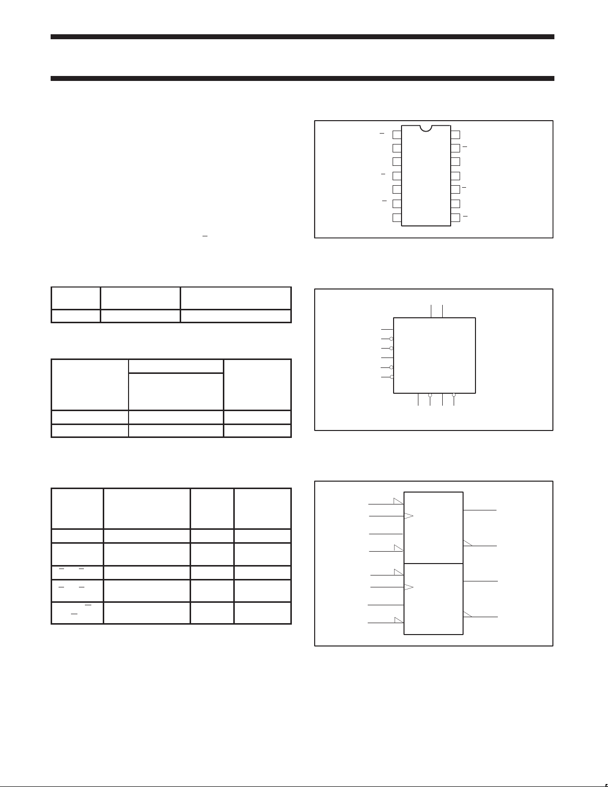
PIN CONFIGURATION
1
R
D0
2
D0
3
CP0
4
SD0
Q0
5
0
Q
6
GND
IEC/IEEE SYMBOL
3
CP0
4
SD0
1
RD0
11
CP1
10
SD1
13
RD1
VCC = Pin 14
GND = Pin 7
SF00582
212
D1D0
Q0 Q0 Q1 Q1
56 98
SF00583
V
14
CC
13
D1
R
D1
12
11
CP1
10
SD1
9
Q1
87
Q1
INPUT AND OUTPUT LOADING AND FAN OUT TABLE
74F
PINS DESCRIPTION
(U.L.)
HIGH/
LOW
D0, D1 Data inputs 1.0/0.417 20µA/250µA
CP0, CP1
Clock inputs (active
rising edge)
1.0/1.0 20µA/20µA
SD0, SD1 Set inputs (active low) 1.0/1.0 20µA/20µA
RD0, RD1
Q0, Q1, Q0,
Q1
Reset inputs (active
low)
Data outputs
1.0/1.0 20µA/20µA
750/33
NOTE: One (1.0) FAST unit load is defined as: 20µA in the high
state and 0.6mA in the low state.
LOAD VAL-
UE HIGH/
LOW
15mA/20mA
LOGIC SYMBOL
4
3
2
1
10
11
12
13
&
S
C1
1D
R
S
C2
2D
R
3
6
9
8
SF00584
September 14, 1990 853-1391 00419
2
Page 3
Philips Semiconductors Product specification
74F5074Synchronizing dual D-type flip-flop/clock driver
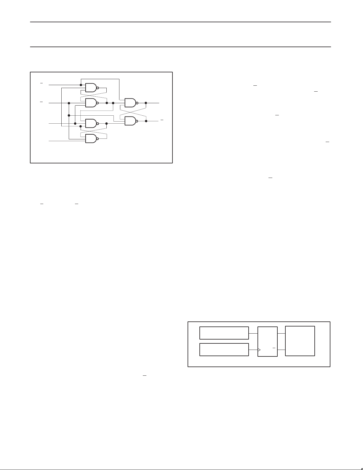
LOGIC DIAGRAM
4, 10
SD
D
R
CP
D
VCC = Pin 14
GND = Pin 7
1, 13
3, 11
2, 12
5, 9
6, 8
SF00585
Q
Q
DESCRIPTION
The 74F5074 is a dual positive edge–triggered D–type featuring
individual data, clock, set and reset inputs; also true and
complementary outputs.
Set (S
Dn) and reset (RDn) are asynchronous active low inputs and
operate independently of the clock (CPn) input. Data must be stable
just one setup time prior to the low–to–high transition of the clock for
guaranteed propagation delays.
Clock triggering occurs at a voltage level and is not directly related
to the transition time of the positive–going pulse. Following the hold
time interval, data at the Dn input may be changed without affecting
the levels of the output.
The 74F5074 is designed so that the outputs can never display a
metastable state due to setup and hold time violations. If setup time
and hold time are violated the propagation delays may be extended
beyond the specifications but the outputs will not glitch or display a
metastable state. Typical metastability parameters for the 74F5074
are: τ ≅ 135ps and T
≅ 9.8 X 10
o
6
sec where τ represents a
function of the rate at which a latch in a metastable state resolves
that condition and T
represents a function of the measurement of
0
the propensity of a latch to enter a metastable state.
Metastable Immune Characteristics
Philips Semiconductor uses the term ’metastable immune’ to
describe characteristics of some of the products in its family.
Specifically the 74F50XXX family presently consist of 4 products
which will not glitch or display an output anomaly under any
circumstances including setup and hold time violations. This claim is
easily verified on the 74F5074. By running two independent signal
generators (see Fig. 1) at nearly the same frequency (in this case
10MHz clock and 10.02 MHz data) the device–under–test can be
often be driven into a metastable state. If the Q output is then used
to trigger a digital scope set to infinite persistence the Q
build a waveform. An experiment was run by continuously operating
the devices in the region where metastability will occur.
output will
When the device–under–test is a 74F74 (which was not designed
with metastable immune characteristics) the waveform will appear
as in Fig. 2.
Figure 2 shows clearly that the Q
output can vary in time with
respect to the Q trigger point. This also implies that the Q or Q
output waveshapes may be distorted. This can be verified on an
analog scope with a charge plate CRT. Perhaps of even greater
interest are the dots running along the 3.5V volt line in the upper
right hand quadrant. These show that the Q
output did not change
state even though the Q output glitched to at least 1.5 volts, the
trigger point of the scope.
When the device–under–test is a metastable immune part, such as
the 74F5074, the waveform will appear as in Fig. 3. The 74F5074 Q
output will appear as in Fig. 3. The 74F5074 Q output will not vary
with respect to the Q trigger point even when the a part is driven into
a metastable state. Any tendency towards internal metastability is
resolved by Philips Semiconductor patented circuitry. If a metastable
event occurs within the flop the only outward manifestation of the
event will be an increased clock–to–Q/Q
propagation delay. This
propagation delay is, of course, a function of the metastability
characteristics of the part defined by τ and T
0.
The metastability characteristics of the 74F5074 and related part
types represent state–of–the–art TTL technology.
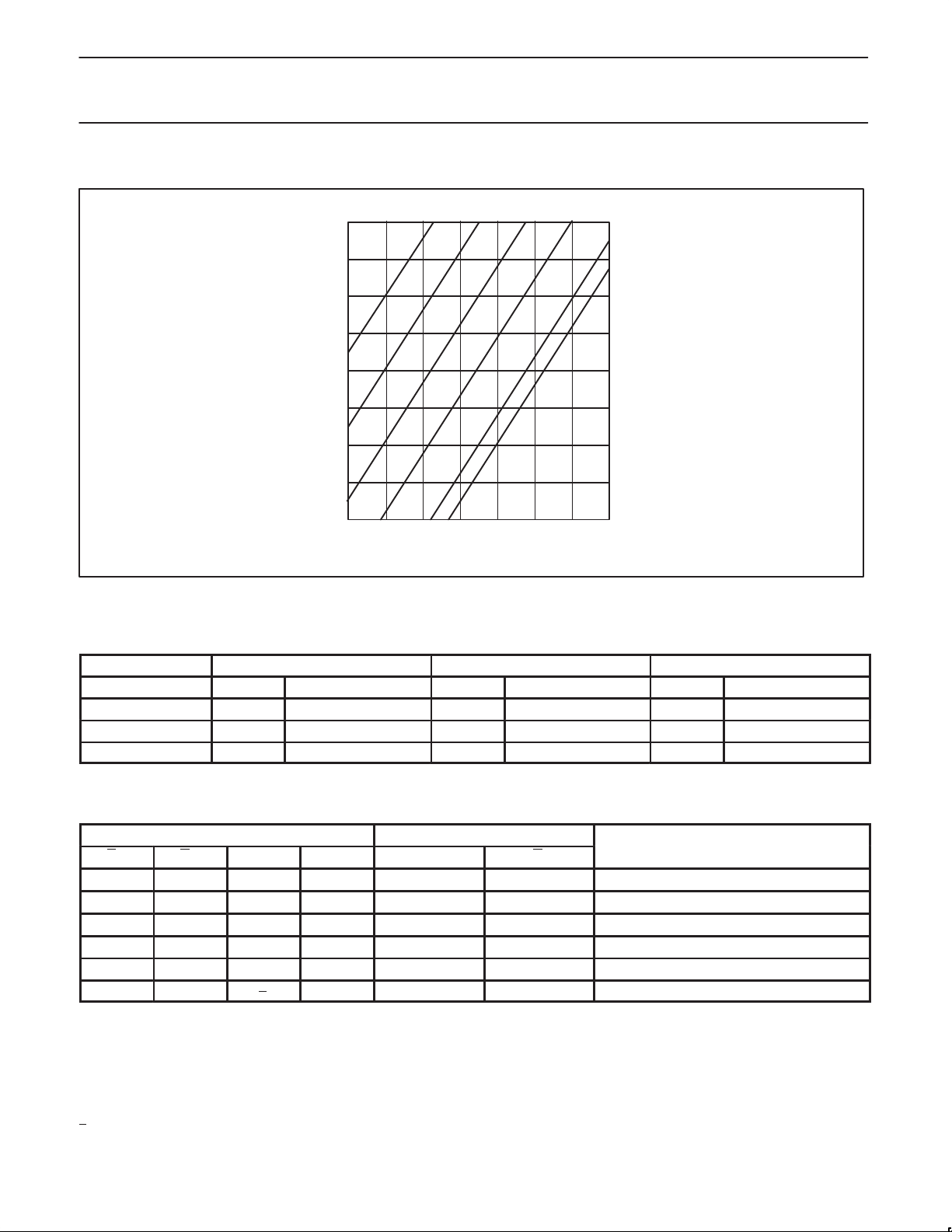
After determining the T
and t of the flop, calculating the mean time
0
between failures (MTBF) is simple. Suppose a designer wants to
use the 74F5074 for synchronizing asynchronous data that is
arriving at 10MHz (as measured by a frequency counter), has a
clock frequency of 50MHz, and has decided that he would like to
sample the output of the 74F5074 10 nanoseconds after the clock
edge. He simply plugs his number into the equation below:
MTBF = e
(t’/t)
/ TofCf
I
In this formula, fC is the frequency of the clock, fI is the average
input event frequency , and t’ is the time after the clock pulse that the
output is sampled (t’ < h, h being the normal propagation delay). In
this situation the f
because input events consist of both of low and high transitions.
Multiplying f
clear that the MTBF is greater than 10
formula the actual MTBF is 1.51 X 10
SIGNAL GENERATOR
SIGNAL GENERATOR
will be twice the data frequency of 20 MHz
I
15
by fC gives an answer of 10
I
Hz2. From Fig. 4 it is
10
seconds. Using the above
10
seconds or about 480 years.
DQ
Q
CP
TRIGGER
DIGITAL
SCOPE
INPUT
SF00586
Figure 1. Test Set-up
September 14, 1990
3
Page 4

Philips Semiconductors Product specification
74F5074Synchronizing dual D-type flip-flop/clock driver
COMP ARISON OF METASTABLE IMMUNE AND NON–IMMUNE CHARACTERISTICS
4
3
2
1
0
Time base = 2.00ns/div Trigger level = 1.5 Volts Trigger slope = positive
Figure 2. 74F74 Q Output triggered by Q output, set-up and hold times violated
3
2
1
0
Time base = 2.00ns/div Trigger level = 1.5 Volts Trigger slope = positive
Figure 3. 74F74 Q Output triggered by Q output, set-up and hold times violated
SF00587
SF00588
September 14, 1990
4
Page 5
Philips Semiconductors Product specification
74F5074Synchronizing dual D-type flip-flop/clock driver
MEAN TIME BETWEEN FAILURES (MTBF) VERSUS t’
6
10,000 years
10
10
10
8
10
10
12
11
10
10
10
10
12
14
10
1015 = fCf
I
100 years
MTBF in seconds
one year
10
10
10
10
9
8
7
6
one week
78910
NOTE: VCC = 5V, T
= 25°C, τ =135ps, To = 9.8 X 10⁶ sec
amb
t’ in nanoseconds
Figure 4.
SF00589
TYPICAL VALUES FOR τ AND T0 AT VARIOUS VCCS AND TEMPERA TURES
T
= 0°C
amb
V
CC
τ T
0
T
= 25°C
amb
τ T
0
5.5V 125ps 1.0 X 10⁹ sec 138ps 5.4 X 10⁶ sec 160ps 1.7 X 10⁵ sec
5.0V 115ps 1.3 X 10¹⁰ sec 135ps 9.8 X 10⁶ sec 167ps 3.9 X 10⁴ sec
4.5V 115ps 3.4 X 10¹³ sec 132ps 5.1 X 10⁸ sec 175ps 7.3 X 10⁴ sec
FUNCTION TABLE
INPUTS OUTPUTS OPERATING
SD RD CP D Q Q MODE
L H X X H L Asynchronous set
H L X X L H Asynchronous reset
L L X X H H Undetermined*
H H ↑ h H L Load “1”
H H ↑ l L H Load “0”
H H ↑ X NC NC Hold
NOTES:
H = High voltage level
h = High voltage level one setup time prior to low–to–high clock transition
L = Low voltage level
l = Low voltage level one setup time prior to low–to–high clock transition
NC= No change from the previous setup
X = Don’t care
↑ = Low–to–high clock transition
= Not low–to–high clock transition
↑
* = This setup is unstable and will change when either set or reset return to the high level
T
= 70°C
amb
τ T
0
September 14, 1990
5
Page 6
Philips Semiconductors Product specification
74F5074Synchronizing dual D-type flip-flop/clock driver
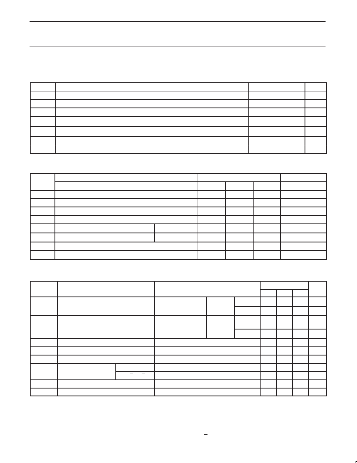
ABSOLUTE MAXIMUM RATINGS
(Operation beyond the limit set forth in this table may impair the useful life of the device. Unless otherwise noted these limits are over the
operating free air temperature range.)
SYMBOL
V
V
I
IN
V
I
OUT
T
T
CC
IN
OUT
amb
stg
Supply voltage –0.5 to +7.0 V
Input voltage –0.5 to +7.0 V
Input current –30 to +5 mA
Voltage applied to output in high output state –0.5 to V
Current applied to output in low output state 40 mA
Operating free air temperature range 0 to +70
Storage temperature range –65 to +150
RECOMMENDED OPERATING CONDITIONS
SYMBOL PARAMETER LIMITS
V
V
V
I
I
I
T
CC
IH
IL
Ik
OH
OL
amb
Supply voltage 4.5 5.0 5.5 V
High–level input voltage 2.0 V
Low–level input voltage 0.8 V
Input clamp current –18 mA
High–level output current
Low–level output current 20 mA
Operating free air temperature range 0 +70
PARAMETER RATING UNIT
CC
V
°C
°C
T
= –40 to +85°C
A
MIN NOM MAX UNIT
VCC ± 10%
VCC ± 5%
–12 mA
–15 mA
°C
DC ELECTRICAL CHARACTERISTICS
(Over recommended operating free-air temperature range unless otherwise noted.)
SYMBOL
V
OH
V
OL
V
IK
I
I
I
IH
I
IL
I
OS
I
CC
High–level output voltage VCC = MIN, VIL =
Low–level output voltage
Input clamp voltage VCC = MIN, II = I
Input current at maximum input voltage VCC = MAX, VI = 7.0V 100 µA
High–level input current VCC = MAX, VI = 2.7V 20 µA
Low–level input current Dn VCC = MAX, VI = 0.5V -250 µA
Short circuit output current
Supply current4 (total) VCC = MAX 20 30 mA
NOTES:
1. For conditions shown as MIN or MAX, use the appropriate value specified under recommended operating conditions for the applicable type.
2. All typical values are at V
3. Not more than one output should be shorted at a time. For testing IOS, the use of high-speed test apparatus and/or sample-and-hold
techniques are preferable in order to minimize internal heating and more accurately reflect operational values. Otherwise, prolonged shorting
of a high output may raise the chip temperature well above normal and thereby cause invalid readings in other parameter tests. In any
sequence of parameter tests, I
4. Measure I
with the clock input grounded and all outputs open, then with Q and Q outputs high in turn.
CC
PARAMETER TEST LIMITS UNIT
MAX,
VIH = MIN
VCC = MIN, VIL =
MAX,
VIH = MIN
CONDITIONS
IK
I
OH
I
OL
1
= MAX
= MAX
±10%V
±5%V
±10%V
±5%V
MIN TYP2MAX
2.5 V
CC
2.7 3.4 V
CC
CC
CC
0.30 0.50 V
0.30 0.50 V
-0.73 -1.2 V
CPn, SDn, RDn VCC = MAX, VI = 0.5V -20 µA
3
= 5V, T
CC
= 25°C.
amb
tests should be performed last.
OS
VCC = MAX -60 -150 mA
September 14, 1990
6
Page 7
Philips Semiconductors Product specification
74F5074Synchronizing dual D-type flip-flop/clock driver
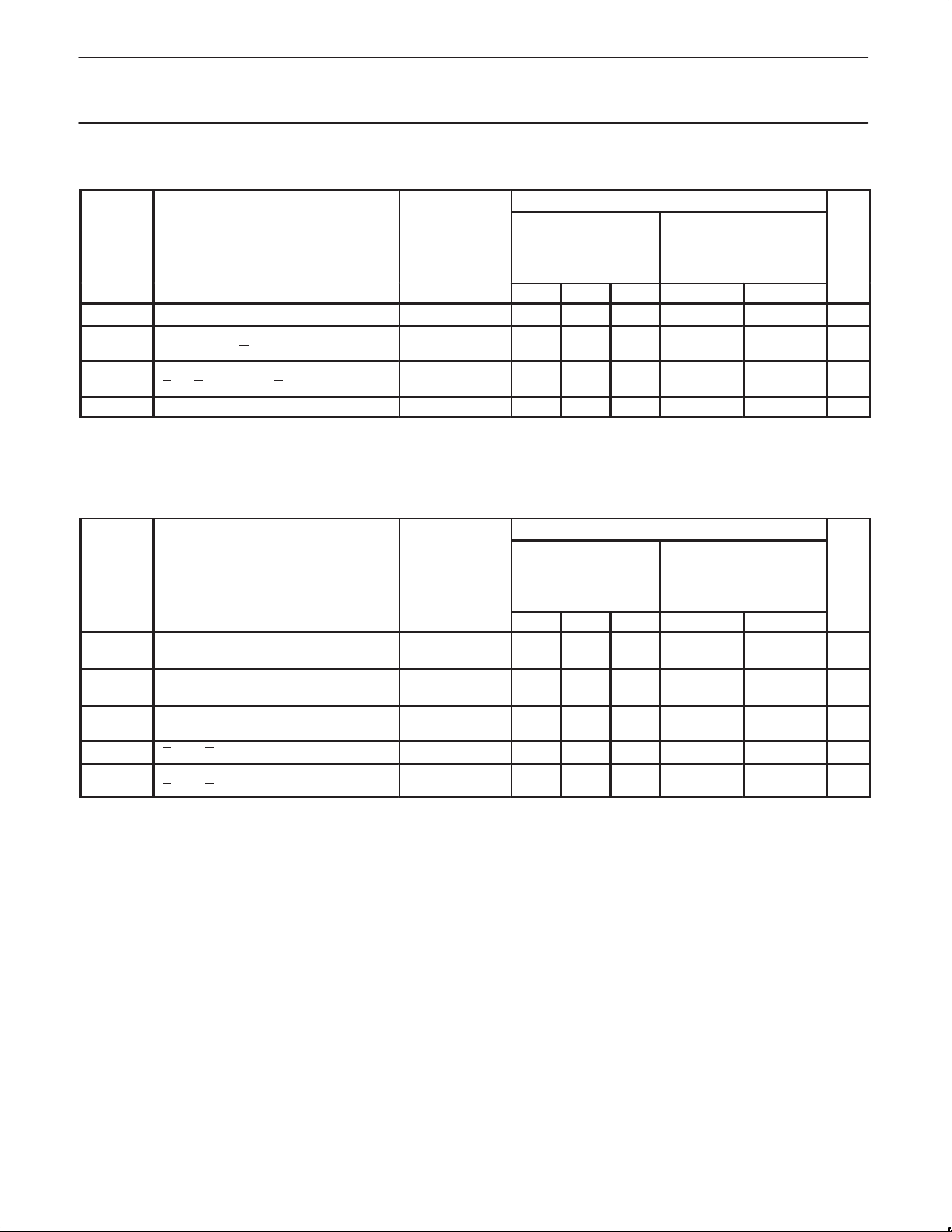
AC ELECTRICAL CHARACTERISTICS
LIMITS
T
= +25°C T
amb
SYMBOL PARAMETER TEST VCC = +5.0V
CONDITION CL = 50pF,
= 500Ω
R
L
MIN TYP MAX MIN MAX
f
max
t
PLH
t
PHL
t
PLH
t
PHL
t
sk(o)
Maximum clock frequency Waveform 1 105 120 90 ns
Propagation delay
CPn to Qn or Qn
Propagation delay
SDn, RDn to Qn or Qn
Output skew
1,2
Waveform 1
Waveform 2
Waveform 4 1.5 1.5 ns
2.0
2.0
3.0
3.0
3.9
3.9
4.5
5.0
NOTES:
1. |t
actual – tPM actual| for any output compared to any other output where N and M are either LH or HL.
PN
2. Skew times are valid only under same test conditions (temperature, V
, loading, etc.,).
CC
6.0
6.0
7.5
7.5
= 0°C to +70°C
amb
VCC = +5.0V ± 10%
CL = 50pF,
= 500Ω
R
L
1.5
2.0
2.5
2.5
6.5
6.5
8.0
8.0
UNIT
ns
ns
AC SETUP REQUIREMENTS
LIMITS
T
= +25°C T
amb
SYMBOL PARAMETER TEST VCC = +5.0V
CONDITION CL = 50pF,
= 500Ω
R
L
MIN TYP MAX MIN MAX
t
(H)
su
tsu(L)
t
(H)
h
t
(L)
h
t
(H)
w
t
(L)
w
t
(L) SDn or RDn pulse width, low Waveform 2 3.0 4.0 ns
w
t
rec
Setup time, high or low
Dn to CPn
Hold time, high or low
Dn to CPn
CPn pulse width,
high or low
Recovery time
SDn or RDn to CPn
Waveform 1
Waveform 1
Waveform 1
1.5
1.5
1.0
1.0
3.0
4.0
Waveform 3 3.0 3.5 ns
= 0°C to +70°C
amb
VCC = +5.0V ± 10%
CL = 50pF,
= 500Ω
R
L
2.0
2.0
1.5
1.5
3.0
4.5
UNIT
ns
ns
ns
September 14, 1990
7
Page 8
Philips Semiconductors Product specification
74F5074Synchronizing dual D-type flip-flop/clock driver
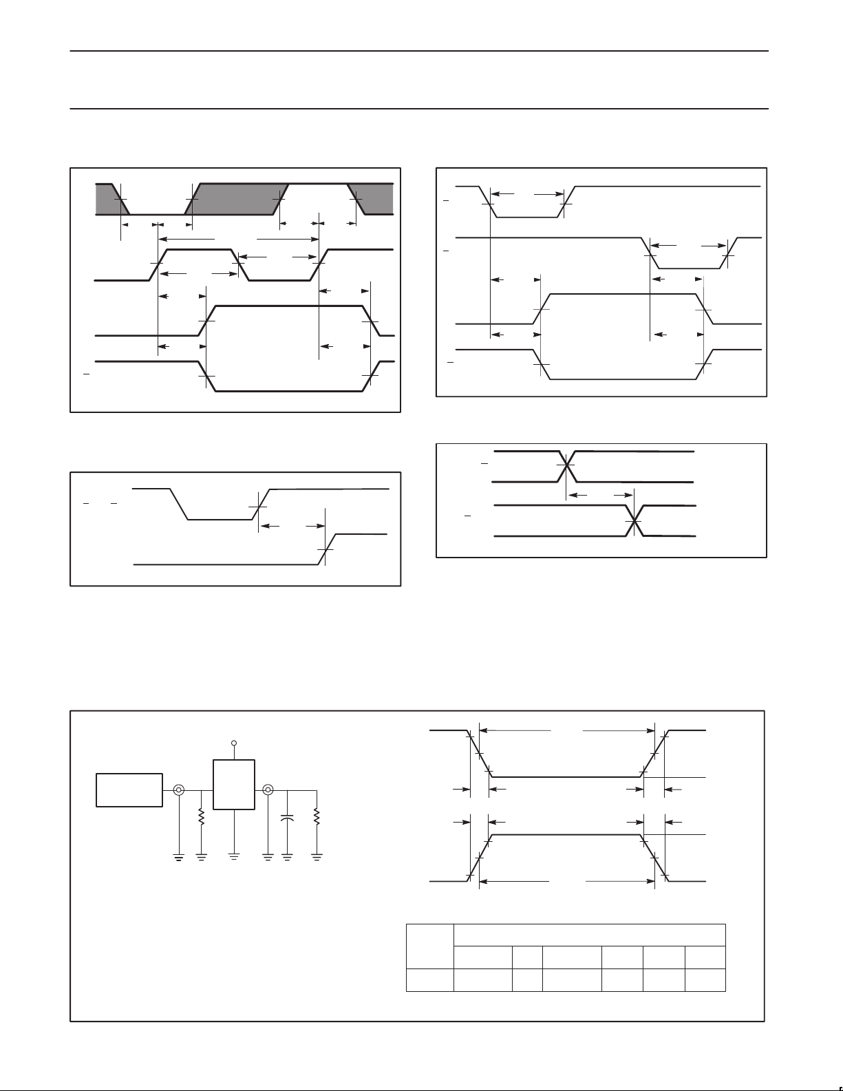
AC WAVEFORMS
Dn
CPn
Qn
Qn
V
V
M
tsu(L) th(L)
V
M
M
t
PLH
t
PHL
tw(H)
V
tsu(H) th(H)
1/f
max
(L)
t
V
M
V
M
V
M
w
V
M
V
M
M
t
PHL
t
PLH
V
V
Waveform 1. Propagation delay for data to output, data
setup time and hold times, and clock
width, and maximum clock frequency
SDn or RDn
CPn
V
M
t
rec
V
M
Waveform 3. Recovery time for set or reset to output
M
M
SF00049
SF00051
t
PLH
t
PHL
tw(L)
V
M
t
(L)
t
PHL
t
PLH
w
V
M
V
M
SF00050
V
M
V
M
V
M
SDn
RDn
Qn
Qn
V
M
Waveform 2. Propagation delay for set and reset to output,
set and reset pulse width
Qn, Qn
Qn, Qn
V
M
t
sk(o)
V
M
SF00590
Waveform 4. Output skew
V
M
NOTES:
For all waveforms, VM = 1.5V.
The shaded areas indicate when the input is permitted to change for predictable output performance.
TEST CIRCUIT AND WAVEFORMS
V
CC
PULSE
GENERATOR
V
IN
R
T
D.U.T.
V
OUT
R
C
L
L
Test Circuit for Totem-Pole Outputs
DEFINITIONS:
R
= Load resistor;
L
see AC ELECTRICAL CHARACTERISTICS for value.
= Load capacitance includes jig and probe capacitance;
C
L
see AC ELECTRICAL CHARACTERISTICS for value.
R
= Termination resistance should be equal to Z
T
pulse generators.
OUT
of
NEGATIVE
PULSE
POSITIVE
PULSE
family
74F
90%
10%
amplitude
V
M
10%
)
t
THL (tf
t
)
TLH (tr
90%
V
M
Input Pulse Definition
INPUT PULSE REQUIREMENTS
V
M
3.0V
1.5V
t
w
t
TLH (tr
t
THL (tf
t
w
rep. rate
1MHz 500ns
10%
)
)
90%
t
w
V
M
V
M
90%
10%
t
TLHtTHL
2.5ns 2.5ns
AMP (V)
0V
AMP (V)
0V
SF00006
September 14, 1990
8
Page 9
Philips Semiconductors Product specification
74F5074Synchronizing dual D-type flip-flop/clock driver
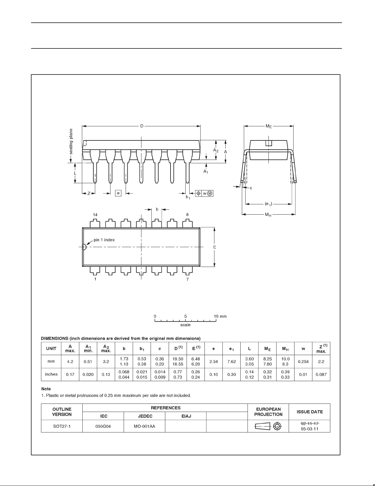
DIP14: plastic dual in-line package; 14 leads (300 mil) SOT27-1
1990 Sep 14
9
Page 10
Philips Semiconductors Product specification
74F5074Synchronizing dual D-type flip-flop/clock driver
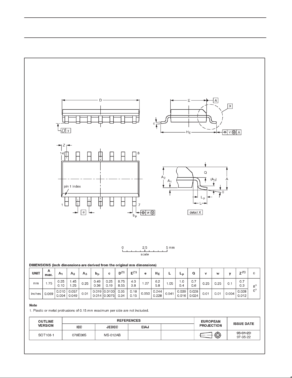
SO14: plastic small outline package; 14 leads; body width 3.9 mm SOT108-1
1990 Sep 14
10
Page 11

Philips Semiconductors Product specification
74F5074Synchronizing dual D-type flip-flop/clock driver
NOTES
1990 Sep 14
11
Page 12
Philips Semiconductors Product specification
74F5074Synchronizing dual D-type flip-flop/clock driver
Data sheet status
Data sheet
status
Objective
specification
Preliminary
specification
Product
specification
Product
status
Development
Qualification
Production
Definition
This data sheet contains the design target or goal specifications for product development.
Specification may change in any manner without notice.
This data sheet contains preliminary data, and supplementary data will be published at a later date.
Philips Semiconductors reserves the right to make chages at any time without notice in order to
improve design and supply the best possible product.
This data sheet contains final specifications. Philips Semiconductors reserves the right to make
changes at any time without notice in order to improve design and supply the best possible product.
[1]
[1] Please consult the most recently issued datasheet before initiating or completing a design.
Definitions
Short-form specification — The data in a short-form specification is extracted from a full data sheet with the same type number and title. For
detailed information see the relevant data sheet or data handbook.
Limiting values definition — Limiting values given are in accordance with the Absolute Maximum Rating System (IEC 134). Stress above one
or more of the limiting values may cause permanent damage to the device. These are stress ratings only and operation of the device at these or
at any other conditions above those given in the Characteristics sections of the specification is not implied. Exposure to limiting values for extended
periods may affect device reliability.
Application information — Applications that are described herein for any of these products are for illustrative purposes only. Philips
Semiconductors make no representation or warranty that such applications will be suitable for the specified use without further testing or
modification.
Disclaimers
Life support — These products are not designed for use in life support appliances, devices or systems where malfunction of these products can
reasonably be expected to result in personal injury . Philips Semiconductors customers using or selling these products for use in such applications
do so at their own risk and agree to fully indemnify Philips Semiconductors for any damages resulting from such application.
Right to make changes — Philips Semiconductors reserves the right to make changes, without notice, in the products, including circuits, standard
cells, and/or software, described or contained herein in order to improve design and/or performance. Philips Semiconductors assumes no
responsibility or liability for the use of any of these products, conveys no license or title under any patent, copyright, or mask work right to these
products, and makes no representations or warranties that these products are free from patent, copyright, or mask work right infringement, unless
otherwise specified.
Philips Semiconductors
811 East Arques Avenue
P.O. Box 3409
Sunnyvale, California 94088–3409
Telephone 800-234-7381
Copyright Philips Electronics North America Corporation 1998
All rights reserved. Printed in U.S.A.
print code Date of release: 10-98
Document order number: 9397-750-05207
yyyy mmm dd
12
 Loading...