

Page 1

Philips Semiconductors Product specification
74F381Arithmetic Logic Unit
1
1989 Mar 01 853–0418 95907
FEATURES
•Low-input loading minimizes drive requirements
•Performs six arithmetic and logic functions
•Selectable Low (clear) and High (preset) functions
•Carry Generate and Propagate outputs for use with Carry
look-ahead generator
DESCRIPTION
The 74F381 performs three arithmetic and three logic operations on
two 4-bit words, A and B. Three additional Select (S0–S2) input
codes force the Function outputs Low or High. Carry Propagate (P
)
and Generate (G
) ouputs are provided for use with the 74F182
Carry Look Ahead Generator for high-speed expansion to longer
word lengths. For ripple expansion, refer to the 74F382 ALU data
sheet.
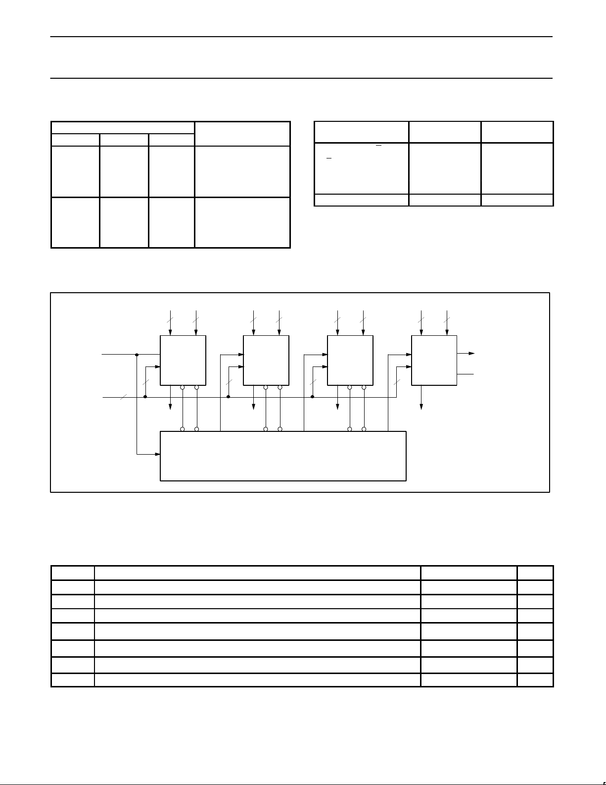
Signals applied to the Select inputs (S0–S2) determine the mode of
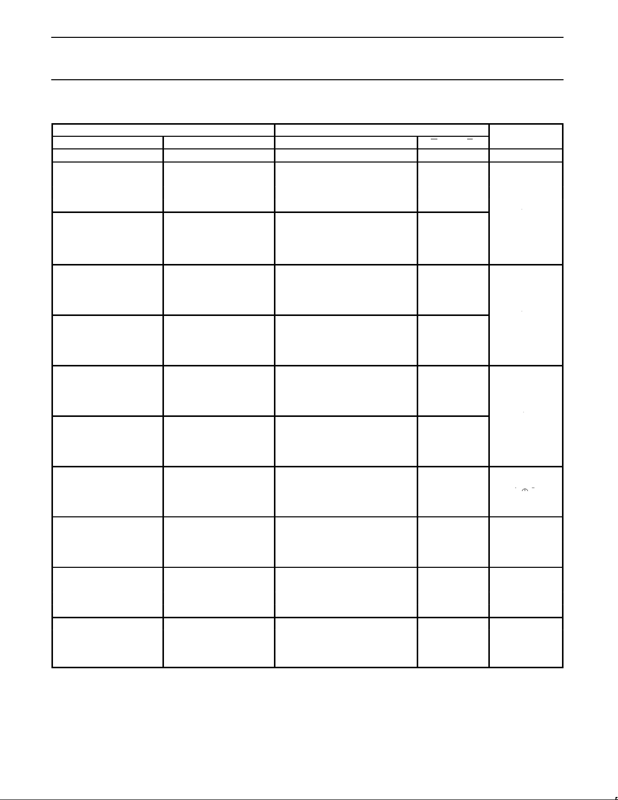
operation, as indicated in the Function Select Table. An extensive
listing of input and output function levels is shown in the Function
Table. The circuit performs the arithmetic functions for either
active-HIgh or active-Low operands, with output levels in the same
convention. In the subtract operating modes, it is necessary to force
a Carry (High for active-HIgh operands, Low for active-Low
operands) into the Cn input of the least significant package. The
Carry Generate (G
) and Carry Propagate (P) outputs supply input
signals to the 74F182 Carry look-ahead generator for expansion to
longer word length, as shown in Figure 1. Note that a 74F382 ALU is
used for the most significant package. Typical delays for Figure 1
are given in Table 1.
PIN CONFIGURATION
20
19
18
17
16
15
147
6
5
4
3
2
1
138
V
CC
A1
B1
A0
B0
S0
S1
S2
F0
F1
GND
A2
B2
A3
B3
Cn
P
G
F3
F2
SF00921
129
1110
TYPICAL
PROPAGATION
DELAY
TYPICAL SUPPL Y
CURRENT (TOTAL)
74F381 6.5ns 59mA
ORDERING INFORMATION
DESCRIPTION
COMMERCIAL RANGE
V
CC
= 5V ±10%, T
amb
= 0°C to +70°C
20-pin plastic DIP N74F381N
20-pin plastic SO N74F381D
INPUT AND OUTPUT LOADING AND FAN OUT TABLE
PINS DESCRIPTION
74F (U.L.)
HIGH/LOW
LOAD VALUE
HIGH/LOW
A0 – A3 A operand inputs 1.0/4.0 20µA/2.4mA
B0 – B3 A operand inputs 1.0/4.0 20µA/2.4mA
S0 – S2 Function select inputs 1.0/1.0 20µA/0.6mA
Cn Carry input 1.0/4.0 20µA/2.4mA
P Carry Propagate ouptut (active-Low) 50/33 1.0mA/20mA
G Carry Generate ouptut (active-Low) 50/33 1.0mA/20mA
F0–F3 Outputs 50/33 1.0mA/20mA
NOTE:
One (1.0) FAST unit load is defined as 20µA in the High state and 0.6mA in the Low state.
TYPE
Page 2
Philips Semiconductors Product specification
74F381Arithmetic Logic Unit
1989 Mar 01
2
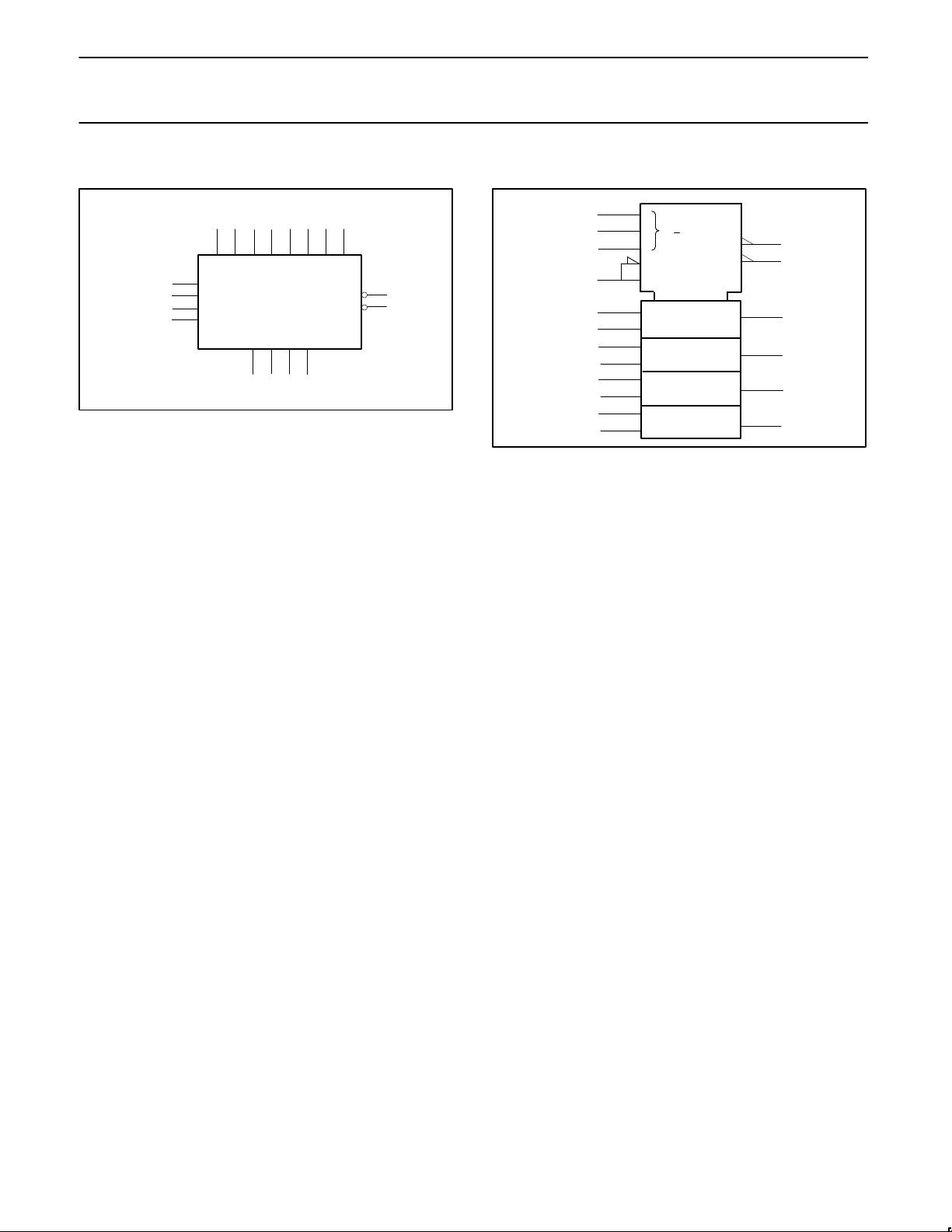
LOGIC SYMBOL
F0 F1 F2 F3
V
CC
= Pin 20
GND = Pin 10
A0 B0 A1 B1 A2 B2 A3 B3
3 4 1 2 19 18 17 16
Cn
S0
S1
S2
15
5
6
7
8 9 11 12
SF00922
G
P
13
14
IEC/IEEE SYMBOL
8
9
11
12
(1/2) Bl
15
P
SF00923
3
4
1
2
19
18
17
16
Q
P
Q
P
Q
P
Q
[1]
[2]
[4]
[8]
0
4
3 Cl
(1/2/3) CP
(1/2/3) CG
M
0
7
5
6
7
14
13
ALU
Page 3
Philips Semiconductors Product specification
74F381Arithmetic Logic Unit
1989 Mar 01
3
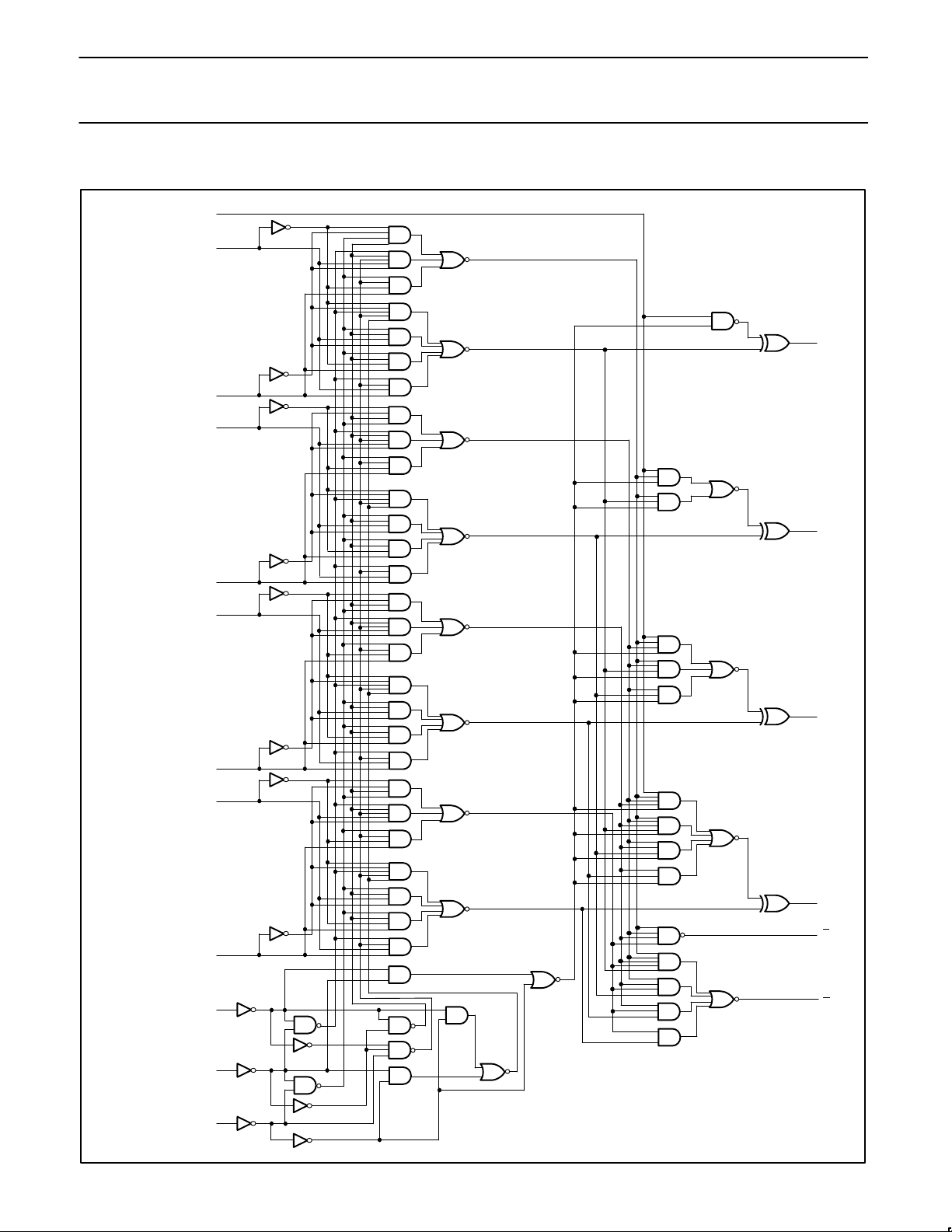
LOGIC DIAGRAM
VCC = Pin 20
GND = Pin 10
3
4
1
2
19
18
17
16
5
6
7
15
Cn
A0
B0
A1
B1
A2
B2
A3
B3
S0
S1
S2
8
9
11
12
14
13
F0
F1
F2
F3
P
G
SF00924
Page 4
Philips Semiconductors Product specification
74F381Arithmetic Logic Unit
1989 Mar 01
4
FUNCTION TABLE
INPUTS OUTPUTS
OPERATING
S0 S1 S2 Cn An Bn F0 F1 F2 F3 G P
OPERATING
MODE
L L L X X X L L L L L L Clear
H L L L L L H H H H H L
H L L L L H L H H H L L
H L L L H L L L L L H H
H L L L H H H H H H H L
H L L H L L L L L L H L
B minus A
H L L H L H H H H H L L
H L L H H L H L L L H H
H L L H H H L L L L H L
L H L L L L H H H H H L
L H L L L H L L L L H H
L H L L H L L H H H L L
L H L L H H H H H H H L
L H L H L L L L L L H L
A minus B
L H L H L H H L L L H H
L H L H H L H H H H L L
L H L H H H L L L L H L
H H L L L L L L L L H H
H H L L L H H H H H H L
H H L L H L H H H H H L
H H L L H H L H H H L L
H H L H L L H L L L H H
A Plus B
H H L H L H L L L L H L
H H L H H L L L L L H L
H H L H H H H H H H L L
L L H X L L L L L L H H
L L H X L H H H H H H H
L L H X H L H H H H H L
A B
L L H X H H L L L L L L
H L H X L L L L L L H H
H L H X L H H H H H H H
H L H X H L H H H H H H
A + B
H L H X H H H H H H H L
L H H X L L L L L L L L
L H H X L H L L L L H H
L H H X H L L L L L L L
AB
L H H X H H H H H H H L
H H H X L L H H H H H H
H H H X L H H H H H H H
H H H X H L H H H H H H
Preset
H H H X H H H H H H H L
H = High voltage level
L = Low voltage level
X = Don’t care
Page 5
Philips Semiconductors Product specification
74F381Arithmetic Logic Unit
1989 Mar 01
5
FUNCTION SELECT TABLE
SELECT
OPERATING
S0 S1 S2
OPERATING
MODE
L L L Clear
H L L B minus A
L H L A minus B
H H L A Plus B
L L H A B
H L H A + B
L H H AB
H H H Preset
H = High voltage level
L = Low voltage level
Table 1. 16-Bit Delay Tabulation
PATH SEGMENT
TOWARD
F
OUTPUT
Cn+4, OVR
Ai or Bi to P 7.2ns 7.2ns
Pi to Cn+i (74F182) 6.2ns 6.2ns
Cn to F 8.1ns –
Cn to Cn+4, OVR – 8.0ns
Total Delay 21.5ns 21.4ns
APPLICATION
A B
Cn
SF00925
C
IN
S
F Q P
74F381
F0–F3
4 4
3
3
A0–A3 B0–B3
G0 P0 Cn+x
A B
Cn
S
F Q P
74F381
F4–F7
4 4
3
A4–A7 B4–B7
G1 P1 Cn+y
A B
Cn
S
F Q P
74F381
F8–F11
4 4
3
A8–A11 B8–B11
G2 P2 Cn+z
A B
Cn
S
F
74F382
F12–F15
4 4
3
A12–A15 B12–B15
Cn+4
OVR
74F182
OVERFLOW
C
OUT
Cn
SELECT
Figure 1. 16-bit Look-ahead Carry ALU Expansion
ABSOLUTE MAXIMUM RATINGS
(Operation beyond the limit set forth in this table may impair the useful life of the device. Unless otherwise noted these limits are over the
operating free-air temperature range.)
SYMBOL
PARAMETER RATING UNIT
V
CC
–0.5 to +7.0 V
V
IN
Input voltage –0.5 to +7.0 V
I
IN
–30 to +1 mA
V
OUT
–0.5 to V
CC
V
I
OUT
40 mA
T
amb
Operating free-air temperature range 0 to +70
°C
T
STG
Storage temperature range –65 to +150
°C
Supply voltage
Input current
Voltage applied to output in High output state
Current applied to output in Low output state
Page 6
Philips Semiconductors Product specification
74F381Arithmetic Logic Unit
1989 Mar 01
6
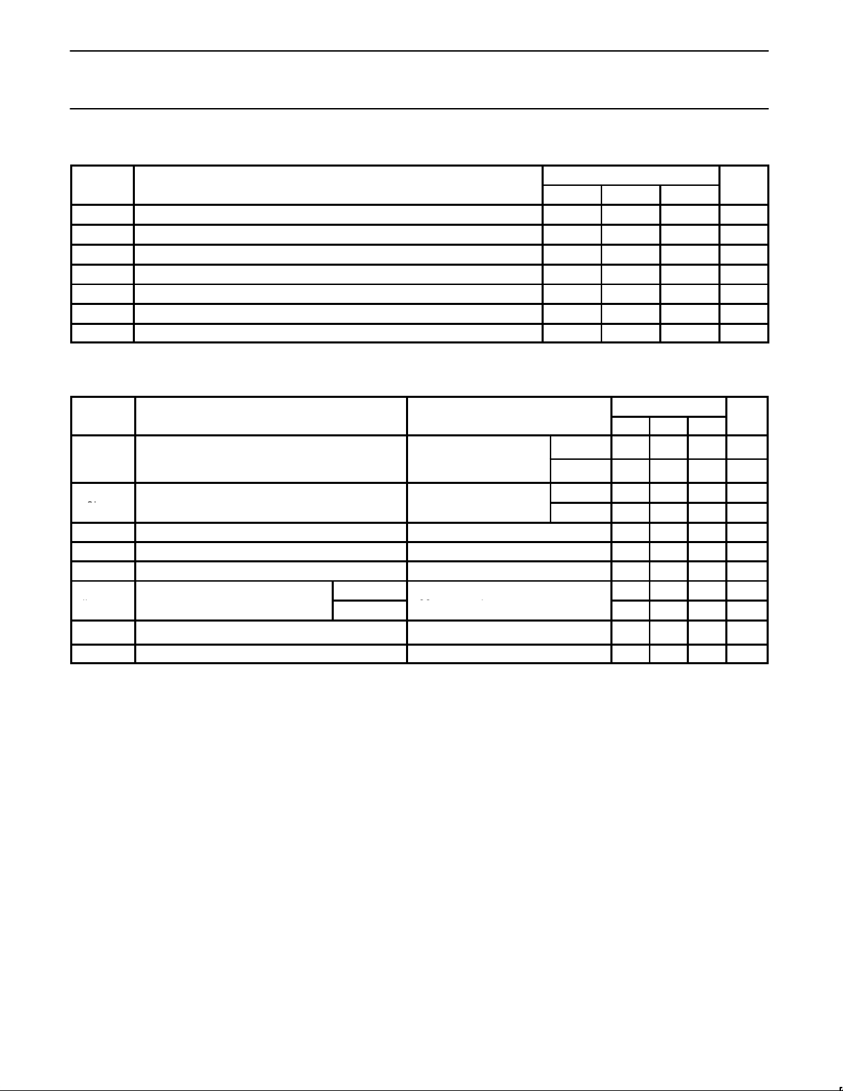
RECOMMENDED OPERATING CONDITIONS
LIMITS
SYMBOL
PARMETER
MIN NOM MAX
UNIT
V
CC
4.5 5.0 5.5 V
V
IH
2.0 V
V
IL
0.8 V
I
IK
–18 mA
I
OH
–1 mA
I
OL
20 mA
T
amb
0 70 °C
DC ELECTRICAL CHARACTERISTICS
(Over recommended operating free-air temperature range unless otherwise noted.)
TEST LIMITS UNIT
SYMBOL
PARAMETER
CONDITIONS
1
MIN TYP2MAX
VCC = MIN, VIL = MAX,
±10%V
CC
2.5 V
VOHHigh-level output voltage
VIH = MIN, IOH = MAX
±5%V
CC
2.7 3.4 V
VCC = MIN, VIL = MAX, ±10%V
CC
0.30 0.50 V
VOLLow-level output voltage
VIH = MIN, IOL = MAX
±5%V
CC
0.30 0.50 V
V
IK
Input clamp voltage VCC = MIN, II = I
IK
–0.73 –1.2 V
I
I
Input current at maximum input voltage VCC = MAX, VI = 7.0V 100 µA
I
IH
High-level input current VCC = MAX, VI = 2.7V 20 µA
An, Bn, Cn
–2.4 mA
IILLow-level input current
S0, S1, S2
VCC = MAX, VI = 0.5V
–0.6 mA
I
OS
3
VCC = MAX –60 –150 mA
I
CC
Supply current (total) VCC = MAX 59 89 mA
NOTES:
1. For conditions shown as MIN or MAX, use the appropriate value specified under recommended operating conditions for the applicable type.
2. All typical values are at V
CC
= 5V, T
amb
= 25°C.
3. Not more than one output should be shorted at a time. For testing I
OS
, the use of high-speed test apparatus and/or sample-and-hold
techniques are preferable in order to minimize internal heating and more accurately reflect operational values. Otherwise, prolonged shorting
of a High output may raise the chip temperature well above normal and thereby cause invalid readings in other parameter tests. In any
sequence of parameter tests, I
OS
tests should be performed last.
SYMBOL
Supply voltage
High-level input voltage
Low-level input voltage
Input clamp current
High-level output current
Low-level output current
Operating free-air temperature range
Short-circuit output current
Page 7
Philips Semiconductors Product specification
74F381Arithmetic Logic Unit
1989 Mar 01
7
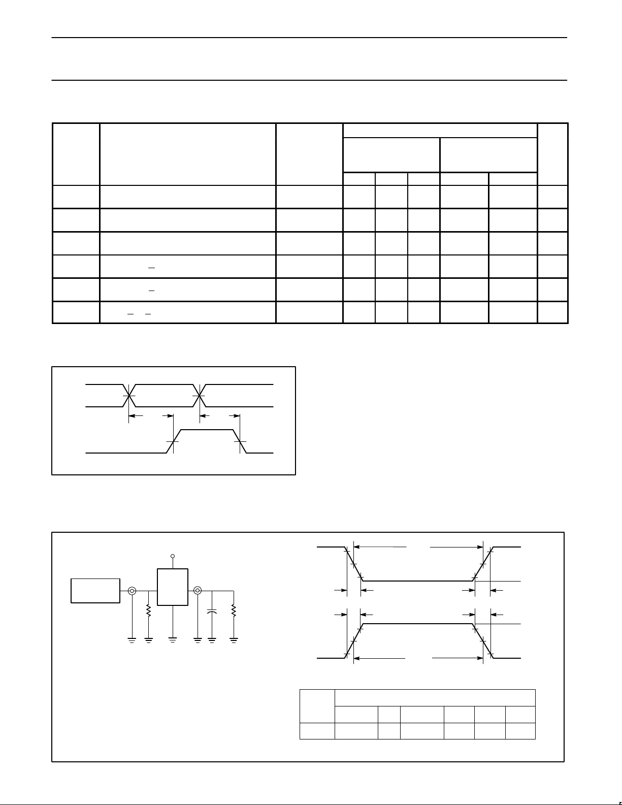
AC ELECTRICAL CHARACTERISTICS
LIMITS
T
amb
= +25°C T
amb
= 0°C to +70°C
SYMBOL PARAMETER TEST VCC = +5.0V VCC = +5.0V ± 10% UNIT
CONDITION CL = 50pF, RL = 500Ω CL = 50pF, RL = 500Ω
MIN TYP MAX MIN MAX
t
PLH
t
PHL
Propagation delay
Cn to Fn
Waveform 1
2.5
2.5
6.0
4.5
11.0
6.5
2.5
2.5
12.5
7.5
ns
t
PLH
t
PHL
Propagation delay
Any An or Bn to any Fn
Waveform 1
3.5
3.0
7.0
6.0
13.0
9.0
3.5
3.0
16.0
10.0
ns
t
PLH
t
PHL
Propagation delay
Sn to Fn
Waveform 1
5.0
4.0
9.0
7.5
20.0
10.5
5.0
4.0
21.5
11.5
ns
t
PLH
t
PHL
Propagation delay
An to Bn to G
Waveform 1
3.5
3.0
6.5
6.0
9.0
8.5
3.5
3.0
10.0
9.0
ns
t
PLH
t
PHL
Propagation delay
An or Bn to P
Waveform 1
3.0
3.5
5.5
6.0
8.0
8.5
3.0
3.5
9.0
9.0
ns
t
PLH
t
PHL
Propagation delay
Sn to G
or P
Waveform 1
5.0
5.5
7.5
8.5
11.0
12.5
5.0
5.0
12.5
14.0
ns
AC WAVEFORMS
For all waveforms, VM = 1.5V.
V
M
V
M
V
M
V
M
V
OUT
V
IN
t
PHL
t
PLH
SF00926
Waveform 1. Propagation Delay for Non-Inverting
or Inverting paths
TEST CIRCUIT AND WAVEFORM
t
w
90%
V
M
10%
90%
V
M
10%
90%
V
M
10%
90%
V
M
10%
NEGATIVE
PULSE
POSITIVE
PULSE
t
w
AMP (V)
0V
0V
t
THL (tf
)
INPUT PULSE REQUIREMENTS
rep. rate
t
w
t
TLHtTHL
1MHz 500ns
2.5ns 2.5ns
Input Pulse Definition
V
CC
family
74F
D.U.T.
PULSE
GENERATOR
R
L
C
L
R
T
V
IN
V
OUT
Test Circuit for Totem-Pole Outputs
DEFINITIONS:
R
L
= Load resistor;
see AC ELECTRICAL CHARACTERISTICS for value.
CL= Load capacitance includes jig and probe capacitance;
see AC ELECTRICAL CHARACTERISTICS for value.
R
T
= Termination resistance should be equal to Z
OUT
of
pulse generators.
t
THL (tf
)
t
TLH (tr
)
t
TLH (tr
)
AMP (V)
amplitude
3.0V
1.5V
V
M
SF00006
 Loading...