

Datasheet 74F245MTCX, 74F245MTC, 74F245MSAX, 74F245MSA, 74F245CW Datasheet (Fairchild Semiconductor)
...Page 1
April 1988
Revised April 1999
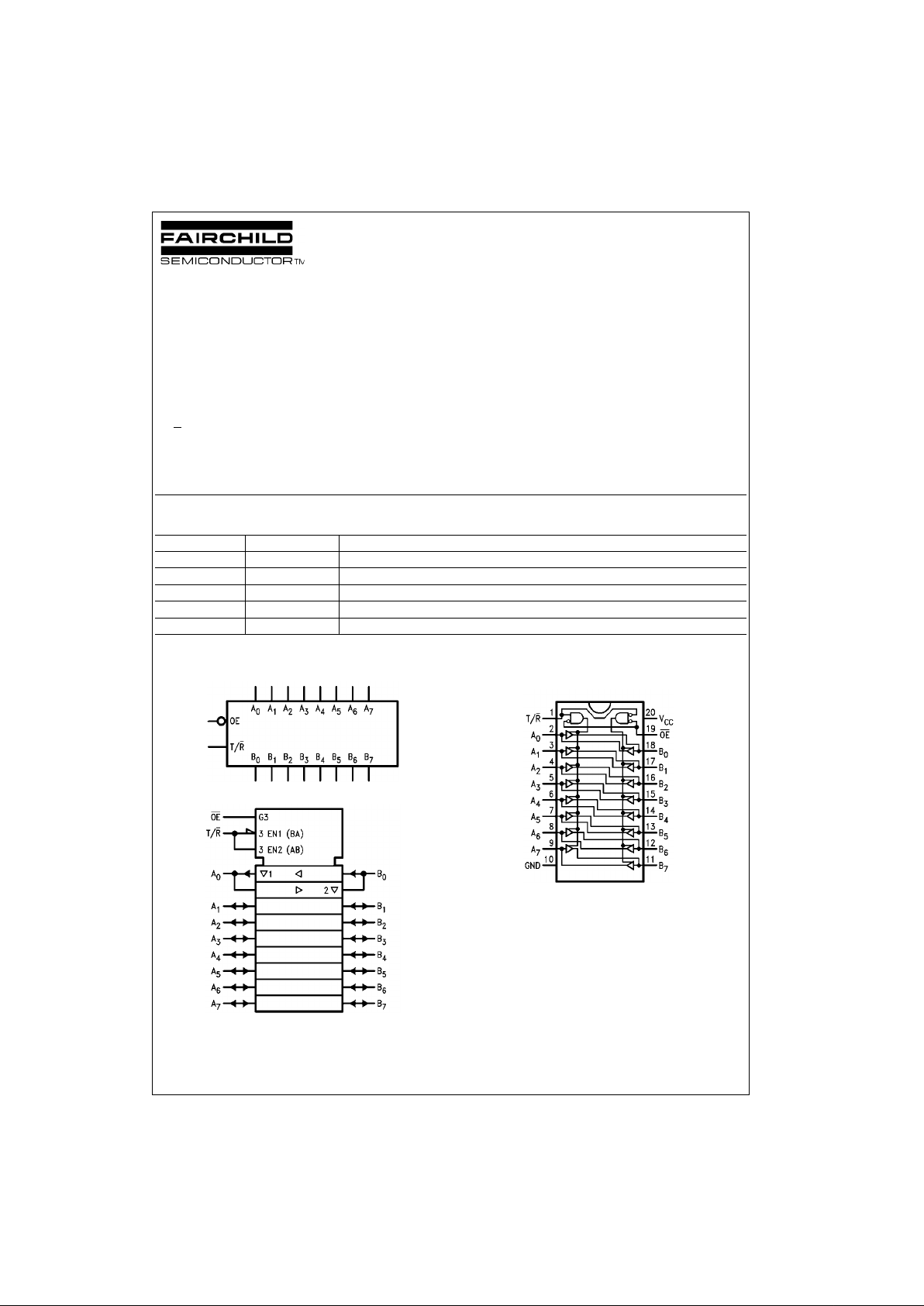
74F245 Octal Bidirectional Transceiver with 3-STATE Outputs
© 1999 Fairchild Semiconductor Corporation DS009503.prf www.fairchildsemi.com
74F245
Octal Bidirectional Transceiver with 3-STATE Outputs
General Description
The 74F245 contains ei ght non-in verting b idirection al buffers with 3-STATE outputs and is intended for bus-ori ented
applications. Current sinking capability is 24 mA at the A
Ports and 64 mA at the B Ports. The Transmit/Receive
(T/R
) input determines the direction of data flow through
the bidirectional transceiver. Transmit (active HIGH)
enables data from A Ports to B Ports; Receive (active
LOW) enables data from B Ports to A Ports. The Outp ut
Enable input, when HIGH, disa bles both A a nd B Por ts by
placing them in a High Z condition.
Features
■ Non-inverting buffers
■ Bidirectional data path
■ A outputs sink 24 mA
■ B outputs sink 64 mA
Ordering Code:
Devices also availab le in Tape and Reel. Specify by appending th e s uffix let t er “X” to the ordering cod e.
Logic Symbols
IEEE/IEC
Connection Diagram
Order Number Package Number Package Description
74F245SC M20B 20-Lead Small Outline Integrated Circuit (SOIC), JEDEC MS-013, 0.300 Wide
74F245SJ M20D 20-Lead Small Outline Package (SOP), EIAJ TYPE II, 5.3mm Wide
74F245MSA MSA20 20-Lead Shrink Small Outline Package (SSOP), EIAJ TYPE II, 5.3mm Wide
74F245MTC MTC20 20-Lead Thin Shrink Small Outline Package (TSSOP), JEDEC MO-153, 4.4mm Wide
74F245PC N20A 20-Lead Plastic Dual-In-Line Package (PDIP), JEDEC MS-001, 0.300 Wide
Page 2
www.fairchildsemi.com 2
74F245
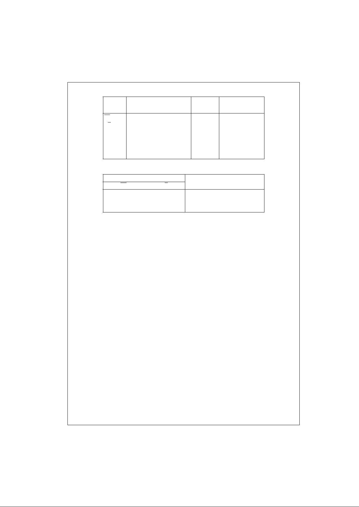
Unit Loading/Fan Out
Truth Table
H = HIGH Voltage Level
L = LOW Voltage Level
X = Immaterial
Pin Names Description
U.L.
Input I
IH/IIL
HIGH/LOW
Output I
OH/IOL
OE Output Enable Input (Active LOW) 1.0/2.0 20 µA/−1.2 mA
T/R
Transmit/Receive Input 1.0/2.0 20 µA/−1.2 mA
A
0–A7
Side A Inputs or 3.5/1.083 70 µA/−0.65 mA
3-STATE Outputs 150/40(38.3) −3 mA/24 mA (20 mA)
B
0–B7
Side B Inputs or 3.5/1.083 70 µA/−0.65 mA
3-STATE Outputs 600/106.6(80) −12 mA/64 mA (48 mA)
Inputs
Output
OE
T/R
L L Bus B Data to Bus A
L H Bus A Data to Bus B
H X High Z State
Page 3
3 www.fairchildsemi.com
74F245
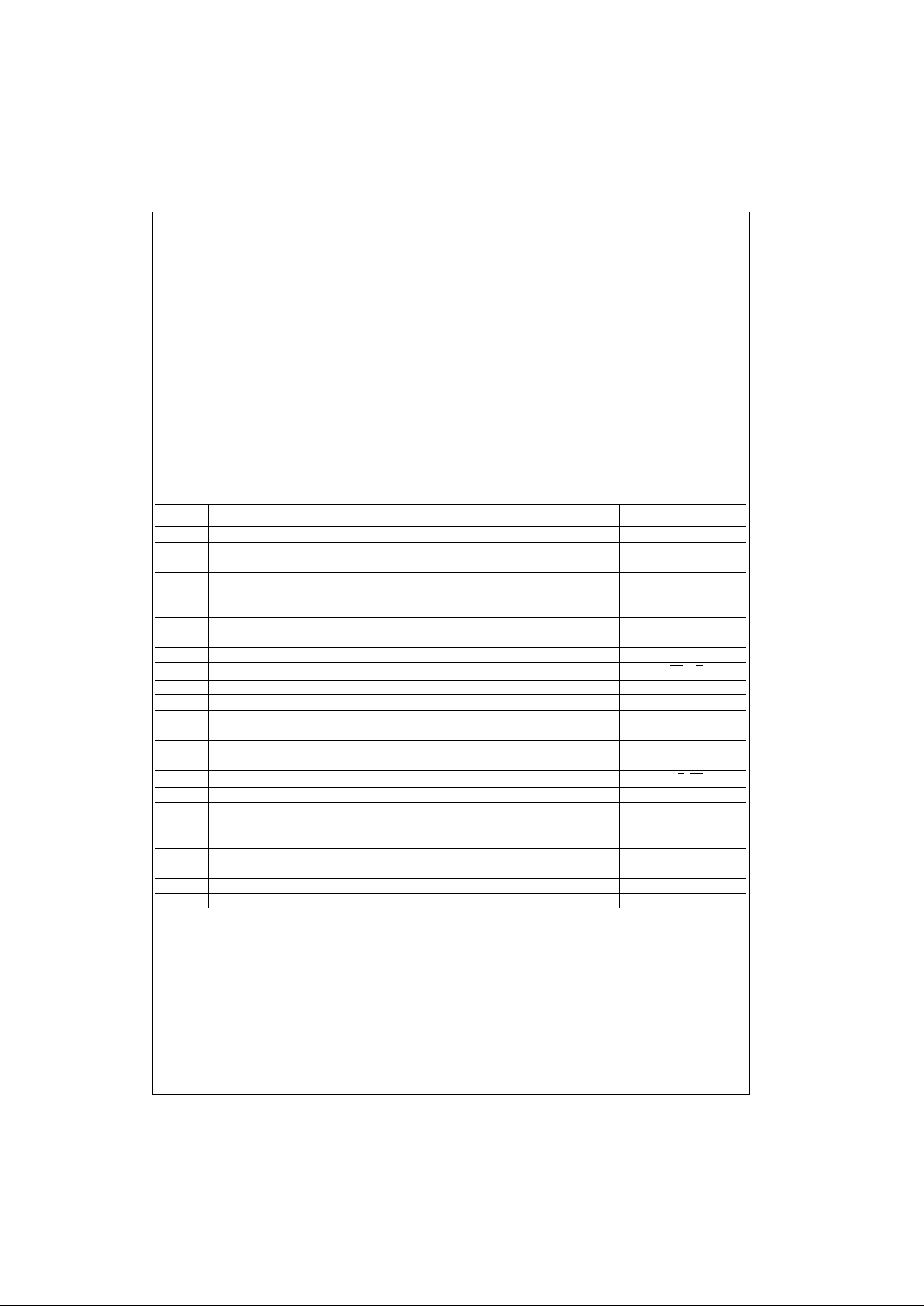
Absolute Maximum Ratings(Note 1) Recommended Operating
Conditions
Note 1: Absolute maximum ratings are values beyon d which the device
may be damaged or have its useful life impaired . Functional operation
under these condit ions is not implied.
Note 2: Either voltage limit or curren t limit is sufficient to protect in puts.
DC Electrical Characteristics
Storage Temperature −65°C to +150°C
Ambient Temperature under Bias −55°C to +125°C
Junction Temperature under Bias −55°C to +150°C
V
CC
Pin Potential to Ground Pin −0.5V to +7.0V
Input Voltage (Note 2) −0.5V to +7.0V
Input Current (Note 2) −30 mA to +5.0 mA
Voltage Applied to Output
in HIGH State (with V
CC
= 0V)
Standard Output −0.5V to V
CC
3-STATE Output −0.5V to +5.5V
Current Applied to Output
in LOW State (Max) twice the r ated I
OL
(mA)
ESD Last Passing Voltage (Min) 4000V
Free Air Ambi ent Temperature 0°C to +70°C
Supply Voltage +4.5V to +5.5V
Symbol Parameter Min Typ Max Units
V
CC
Conditions
V
IH
Input HIGH Voltage 2.0 V Recognized as a HIGH Signal
V
IL
Input LOW Voltage 0.8 V Recognized as a LOW Signal
V
CD
Input Clamp Diode Voltage −1.2 V Min IIN = −18 mA
V
OH
Output HIGH Voltage 10% V
CC
2.4 V Min IOH = −3 mA (An)
10% V
CC
2.0 IOH = −15 mA (Bn)
5% V
CC
2.7 IOH = −3 mA (An)
V
OL
Output LOW Voltage 10% V
CC
0.5 V Min IOL = 24 mA (An)
10% V
CC
0.55 IOL = 64 mA (Bn)
I
IH
Input HIGH Current 5.0 µAMaxVIN = 2.7V
I
BVI
Input HIGH Current Breakdown Test 7.0
µAMax
VIN = 7.0V (OE, T/R)
I
BVIT
Input HIGH Current Breakdown (I/O) 0.5 mA Max VIN = 5.5 V (An, Bn)
I
CEX
Output HIGH Leakage Current 50 µAMaxV
OUT
= VCC (An, Bn)
V
ID
Input Leakage 4.75 V 0.0 IID = 1.9 µA
Test All Other Pins Grounded
I
OD
Output Leakage 3.75 µA0.0V
IOD
= 150 mV
Circuit Current All Other Pins Grounded
I
IL
Input LOW Current −1.2 mA Max
VIN = 0.5V (T/R, OE)
IIH + I
OZH
Output Leakage Current 70 µAMaxV
OUT
= 2.7V (An, Bn)
IIL + I
OZL
Output Leakage Current −650 µAMaxV
OUT
= 0.5V (An, Bn)
I
OS
Output Short-Circuit Current −60 −150 mA Max V
OUT
= 0V (An)
−100 −225 V
OUT
= 0V (Bn)
I
ZZ
Bus Drainage Test 500 µA0.0VV
OUT
= 5.25V(An, Bn)
I
CCH
Power Supply Current 70 90 mA Max VO = HIGH
I
CCL
Power Supply Current 95 120 mA Max VO = LOW
I
CCZ
Power Supply Current 85 110 mA Max VO = HIGH Z
Page 4

www.fairchildsemi.com 4
74F245
AC Electrical Characteristics
Symbol Parameter
TA = +25°CT
A
= − 55°C to +125°CTA = 0°C to +70°C
Units
VCC = +5.0V CL = 50 pF CL = 50 pF
CL = 50 pF
Min Typ Max Min Max Min Max
t
PLH
Propagation Delay 2.5 4.2 6.0 2.0 7.5 2.0 7.0 ns
t
PHL
An to Bn or Bn to A
n
2.54.26.02.07.52.07.0
t
PZH
Output Enable Time 3.0 5.3 7.0 2.5 9.0 2.5 8.0
t
PZL
3.5 6.0 8.0 3.0 10.0 3.0 9.0 ns
t
PHZ
Output Disable Time 2.0 5.0 6.5 2.0 9.0 2.0 7.5
t
PLZ
2.0 5.0 6.5 2.0 10.0 2.0 7.5
Page 5

5 www.fairchildsemi.com
74F245
Physical Dimensions inches (millimeters) unless otherwise noted
20-Lead Small Outline Integrated Circuit (SOIC), JEDEC MS-013, 0.300 Wide
Package Number M20B
20-Lead Small Outline Package (SOP), EIAJ TYPE II, 5.3mm Wide
Package Number M20D
Page 6

www.fairchildsemi.com 6
74F245
Physical Dimensions inches (millimeters) unless otherwise noted (Continued)
20-Lead Shrink Small Outline Package (SSOP), EIAJ TYPE II, 5.3mm Wide
Package Number MSA20
Page 7

7 www.fairchildsemi.com
74F245
Physical Dimensions inches (millimeters) unless otherwise noted (Continued)
20-Lead Thin Shrink Small Outline Package (TSSOP), JEDEC MO-153, 4.4mm Wide
Package Number MTC20
Page 8

Fairchild does not assume any responsibility for use of any circuitry described, no circuit patent licenses are implied and Fairchild reserves the right at any time without notice to change said circuitry and specifications.
74F245 Octal Bidirectional Transceiver with 3-STATE Outputs
LIFE SUPPORT POLICY
FAIRCHILD’S PRODUCTS ARE NOT AUTHORIZED FOR USE AS CRITICAL COMPONENTS IN LIFE SUPPORT
DEVICES OR SYSTEMS WITHOUT THE EXPRESS WRITTEN APPROVAL OF THE PRESIDENT OF FAIRCHILD
SEMICONDUCTOR CORPORATION. As used herein:
1. Life support devices or systems are devices or systems
which, (a) are intended for surgical implant into the
body, or (b) support or sustain life, and (c) whose failure
to perform when properly used in accordance with
instructions for use provided in the labeling, can be reasonably expected to result in a significant inju ry to the
user.
2. A critical component in any componen t of a life su pport
device or system whose failu re to perform can be reasonably expected to ca use the fa i lure of the life su pp ort
device or system, or to affect its safety or effectiveness.
www.fairchildsemi.com
Physical Dimensions inches (millimeters) unless otherwise noted (Continued)
20-Lead Plastic Dual-In-Line Package (PDIP), JEDEC MS-001, 0.300 Wide
Package Number N20A
 Loading...