

Page 1
74F182
Carry Lookahead Generator
74F182 Carry Lookahead Generator
April 1988
Revised July 1999
General Description
The 74F182 is a high-speed carry lookah ead genera tor. It
is generally used w ith the 74F181 or 74F381 4-bit ari thmetic logic units to provide high-speed lookahead over
word lengths of more than four bits.
Features
■ Provides lookahead carries across a group of four ALUs
■ Multi-level lookahead high-speed arithmetic operation
over long word lengths
Ordering Code:
Order Number Package Number Package Description
74F182SJ M16D 16-Lead Small Outline Package (SOP), EIAJ TYPE II, 5.3mm Wide
74F182PC N16E 16-Lead Plastic Dual-In-Line Package (PDIP), JEDEC MS-001, 0.300 Wide
Devices also availab le in Tape and Reel. Specify by appending th e s uffix let t er “X” to the ordering cod e.
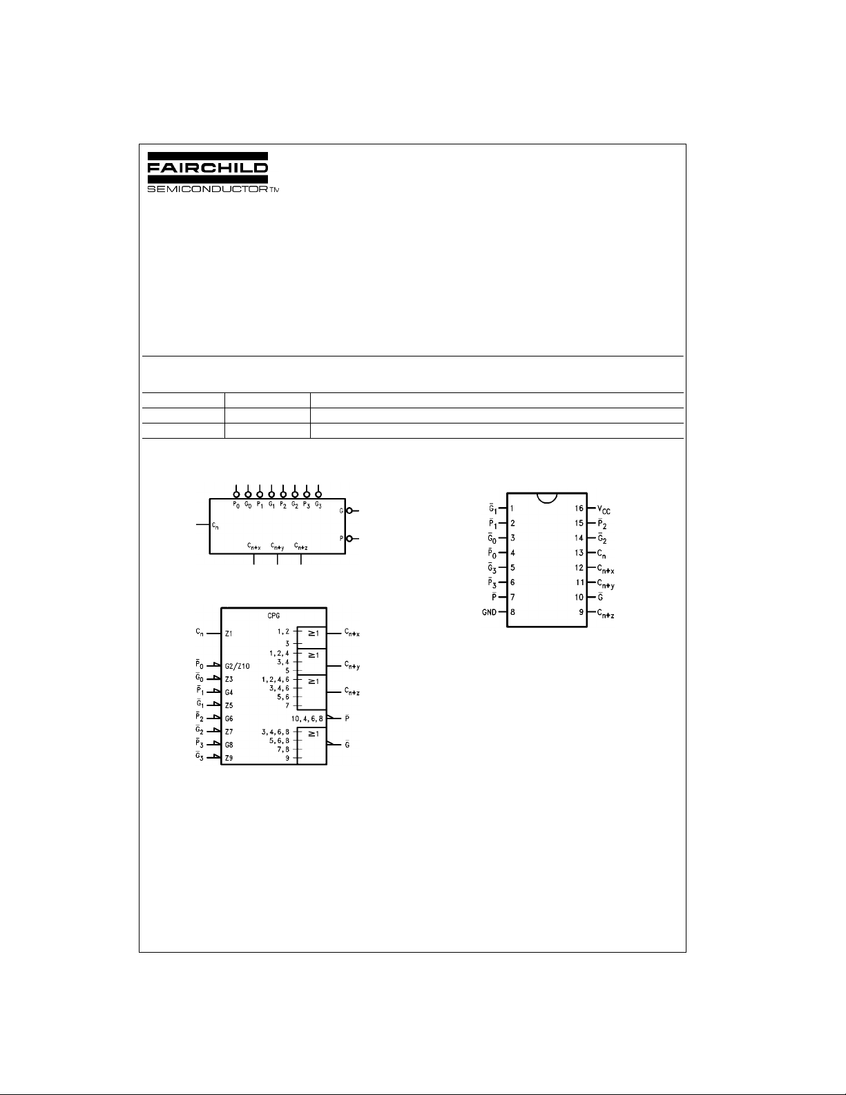
Logic Symbols Connection Diagram
© 1999 Fairchild Semiconductor Corporation DS009492 www.fairchildsemi.com
Page 2
Unit Loading/Fan Out
74F182
Pin Names Description
C
n
, G
G
0
G
1
G
3
, P
P
0
1
P
2
P
3
− C
C
n+x
G
P
Carry Input 1.0/2.0 20 µA/−1.2 mA
Carry Generate Inputs (Active LOW) 1.0/14.0 20 µA/−8.4 mA
2
Carry Generate Input (Active LOW) 1.0/16.0 20 µA/−9.6 mA
Carry Generate Input (Active LOW) 1.0/8.0 20 µA/−4.8 mA
Carry Propagate Inputs (Active LOW) 1.0/8.0 20 µA/−4.8 mA
Carry Propagate Input (Active LOW) 1.0/6.0 20 µA/−3.6 mA
Carry Propagate Input (Active LOW) 1.0/4.0 20 µA/−2.4 mA
Carry Outputs 50/33.3 −1 mA/20 mA
n+z
Carry Generate Output (Active LOW) 50/33.3 −1 mA/20 mA
Carry Propagate Output (Active LOW) 50/33.3 −1 mA/20 mA
Functional Description
The 74F182 carry lookahe ad generator acce pts up to four
pairs of Active LOW Carry Propagate (P
Generate (G
) and provides anticip ated Active HIGH carries (C
(C
n
, C
C
n+y
) signals and an Active HIGH Carr y input
0–G3
) across four groups of binary adders. The
n+z
74F182 also has Active LOW Carry Propagate (P
Carry Generate (G
) outputs which may be use d for furthe r
levels of lookahead . The logic equations provided at the
outputs are:
= G0 + P0 C
C
n+x
C
= G1 + P1 G0 + P1 P0 C
n+y
C
= G2 + P2 G1 + P2 P1 G0 + P2 P1 P0 C
n+z
n
n
G = G3 + P3 G2 + P3 P2 G1 + P3 P2 P1 G
P = P2 P2 P1 P
0
0–P3
n
0
) and Carry
n + x
) and
U.L.
HIGH/LOW
Input I
Output I
IH/IIL
OH/IOL
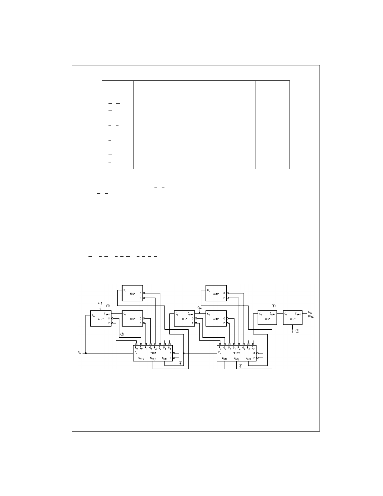
Also, the 74F182 can be used with binary ALUs in an
active LOW or active HIGH input ope rand mode . The connections (Figure 1) to and from the ALU to the carry lookahead generator are identical in both cases. Carries are
,
rippled between lookahea d blocks. Th e critical speed p ath
follows the circled numbers. There are several possible
arrangements for the carry interconnects, but all ach ieve
about the same speed. A 28-bit ALU is formed by dropping
the last 74F181 or 74F381.
*ALUs may be either 74F181 or 74F381
FIGURE 1. 32-Bit ALU with Rippled Carry between 16-Bit Lookahead ALUs
www.fairchildsemi.com 2
Page 3
Truth Table
Inputs Outputs
C
nG0P0G1P1G2P2G3P3Cn+xCn+yCn+z
XHH L
LHX L
XLX H
HXL H
XXXHH L
XHHHX L
LHXHX L
XXXLX H
XLXXL H
HXLXL H
XXXXXHH L
XXXHHHX L
XHHHXHX L
LHXHXHX L
XXXXXLX H
XXXLXXL H
XLXXLXL H
HXLXLXL H
74F182
G P
H = HIGH Voltage Level
L = LOW Voltage Level
X = Immaterial
X XXXXHH H
X XXHHHX H
X HHHXHX H
H HXHXHX H
X XXXXLX L
XXXLXXL L
XLXXLXL L
L XLXLXL L
HXXX H
XHXX H
XXHX H
XXXH H
LLLL L
3 www.fairchildsemi.com
Page 4

Logic Diagram
74F182
Please note that this diagram is provided o nly f or t he understanding of lo gic operations and shou ld not be used to estimate propagation delays.
www.fairchildsemi.com 4
Page 5

Absolute Maximum Ratings(Note 1) Recommended Operating
Storage Temperature −65°C to +150°C
Ambient Temperature under Bias −55°C to +125°C
Junction Temperature under Bias −55°C to +150°C
Pin Potential to Ground Pin −0.5V to +7.0V
V
CC
Input Voltage (Note 2) −0.5V to +7.0V
Input Current (Note 2) −30 mA to +5.0 mA
Voltage Applied to Output
in HIGH State (with V
CC
= 0V)
Standard Output −0.5V to V
3-STATE Output −0.5V to +5.5V
Current Applied to Output
in LOW State (Max) twice the rated I
OL
ESD Last Passing Voltage (Min) 4000V
Conditions
Free Air Ambient Temperature 0°C to +70°C
Supply Voltage +4.5V to +5.5V
Note 1: Absolute maximum ratings are values beyon d which the device
CC
may be damaged or have its useful life impaired . Functional operation
under these condit ions is not implied.
Note 2: Either voltage limit or curren t limit is sufficient to protect in puts.
(mA)
DC Electrical Characteristics
74F182
Symbol Parameter Min Typ Max Units
V
V
V
V
V
I
IH
I
BVI
I
CEX
V
I
OD
I
IL
I
OS
I
CCH
I
CCL
IH
IL
CD
OH
OL
ID
Input HIGH Voltage 2.0 V Recognized as a HIGH Signal
Input LOW Voltage 0.8 V Recognized as a LOW Signal
Input Clamp Diode Voltage −1.2 V Min IIN = −18 mA
Output HIGH 10% V
Voltage 5% V
Output LOW 10% V
Voltage
Input HIGH
Current
Input HIGH Current
Breakdown Test
Output HIGH
Leakage Current
Input Leakage
Test All Other Pins Grounded
Output Leakage
Circuit Current All Other Pins Grounded
Input LOW −1.2
Current −2.4
Output Short-Circuit Current −60 −150 mA Max V
Power Supply Current 18.4 28.0 mA Max VO = HIGH
Power Supply Current 23.5 36.0 mA Max VO = LOW
2.5
CC
2.7 IOH = −1 mA
CC
CC
4.75 V 0.0
0.5 V Min IOL = 20 mA
5.0 µAMaxVIN = 2.7V
7.0 µAMaxVIN = 7.0V
50 µAMaxV
3.75 µA0.0
−3.6
−4.8
−8.4
−9.6
V
CC
VMin
mA Max
Conditions
IOH = −1 mA
= V
OUT
CC
IID = 1.9 µA
V
= 150 mV
IOD
VIN = 0.5V (Cn)
VIN = 0.5V (P3)
VIN = 0.5V (P2)
VIN = 0.5V (G3, P0, P1)
VIN = 0.5V (G0, G2)
VIN = 0.5V (G1)
= 0V
OUT
5 www.fairchildsemi.com
Page 6

AC Electrical Characteristics
74F182
Symbol Parameter
t
PLH
t
PHL
t
PLH
t
PHL
t
PLH
t
PHL
t
PLH
t
PHL
t
PLH
t
PHL
t
PLH
t
PHL
Propagation Delay 3.0 6.6 8.5 3.0 12.0 3.0 9.5
Cn to C
, C
, C
n+x
n+y
n+z
Propagation Delay 2.5 6.2 8.0 2.5 11.0 2.5 9.0
P0, P1, or P2 to
C
, C
, or C
n+x
n+y
n+z
Propagation Delay 2.5 6.5 8.5 2.5 11.0 2.5 9.5
G0, G1, or G2 to
C
, C
, or C
n+x
n+y
n+z
Propagation Delay 3.0 7.9 10.0 3.0 12.0 3.0 11.0
P1, P2, or P3 to G
Propagation Delay 3.0 8.3 10.5 3.0 12.0 3.0 11.5
Gn to G
Propagation Delay 3.0 5.7 7.5 2.5 10.0 3.0 8.5
Pn to P
TA = +25°CT
= −55°C to +125°CTA = 0°C to +70°C
A
VCC = +5.0V VCC = +5.0V VCC = +5.0V
CL = 50 pF CL = 50 pF CL = 50 pF
Min Typ Max Min Max Min Max
3.0 6.8 9.0 3.0 11.0 3.0 10.0
1.53.75.01.07.01.56.0
1.53.95.21.07.01.56.0
3.0 6.0 8.0 2.5 10.0 3.0 9.0
3.0 5.7 7.5 2.5 10.0 3.0 8.5
2.54.15.52.58.02.56.5
Units
ns
ns
ns
ns
ns
ns
www.fairchildsemi.com 6
Page 7

Physical Dimensions inches (millimeters) unless otherwise noted
74F182
16-Lead Small Outline Package (SOP), EIAJ TYPE II, 5.3mm Wide
Package Number M16D
7 www.fairchildsemi.com
Page 8

Physical Dimensions inches (millimeters) unless otherwise noted (Continued)
74F182 Carry Lookahead Generator
16-Lead Plastic Dual-In-Line Package (PDIP), JEDEC MS-001, 0.300 Wide
Fairchild does not assume any responsibility for us e of any circuitry described, no circuit patent licenses are implied and
Fairchild reserves the right at any time without notice to change said circuitry and specifications.
LIFE SUPPORT POLICY
FAIRCHILD’S PRODUCTS ARE NOT AUTHORIZED FOR USE AS CRITICAL COMPONENTS IN LIFE SUPPORT
DEVICES OR SYSTEMS WITHOUT THE EXPRESS WRITTEN APPROVAL OF THE PRESIDENT OF FAIRCHILD
SEMICONDUCTOR CORPORATION. As used herein:
1. Life support devices or systems are devices or syste ms
which, (a) are intended for surgical implant into the
body, or (b) support or sustain life, and (c) whose failure
to perform when properly used in accordance with
instructions for use provided in the labeling, can be reasonably expected to result in a significan t injury to the
user.
Package Number N16E
2. A critical component in any compon ent of a lif e supp ort
device or system whose failu re to perform can be reasonably expected to ca use the fa i lure of the li fe su pp ort
device or system, or to affect its safety or effectiveness.
www.fairchildsemi.com
www.fairchildsemi.com 8
 Loading...