

Page 1
Philips Semiconductors Product specification
74F182Look-ahead carry generator
2
1991 Apr 15 853–1161 02162
FEATURES
•Provides carry look-ahead across a group of four ALUs
•Multi-level look-ahead for high speed arithmetic operation over
long word lengths
DESCRIPTION
The 74F182 is a high speed carry look-ahead generator. It accepts
up to four pairs of active-Low Carry Propagate (P
0, P1, P2, P3) and
Carry Generate (G
0, G1, G2, G3) signals and an active-High Carry
input (Cn) and provides anticipated active-High carries (Cn+x, Cn+y,
Cn+z) across four groups of binary adders. The 74F182 also has
active-Low Carry Propagate (P
) Carry Generate (G) outputs which
may be used for further levels of look-ahead.
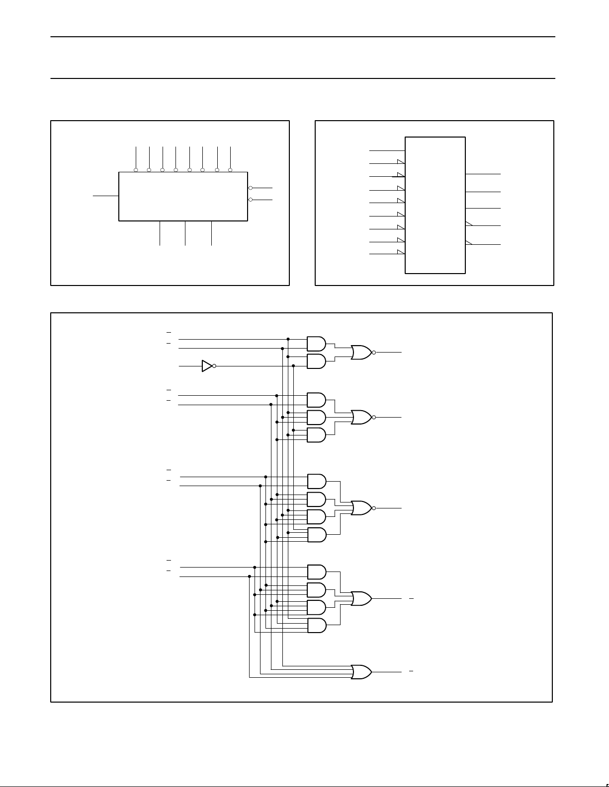
The logic equations provided at the outputs are:
Cn+x = G0+P0Cn
Cn+y = G1+P1G0+P1P0Cn
Cn+z = G2+P2G1+P2P1G0+P2P1P0Cn
G
= G3+P3G2+P3P2G1+P3P2P1G0
P
= P3P2P1P0
The 74F182 can also be used with binary ALUs in an active-Low or
active-High input operand mode. The connections to and from the
ALU to the carry look-ahead generator are identical in both cases.
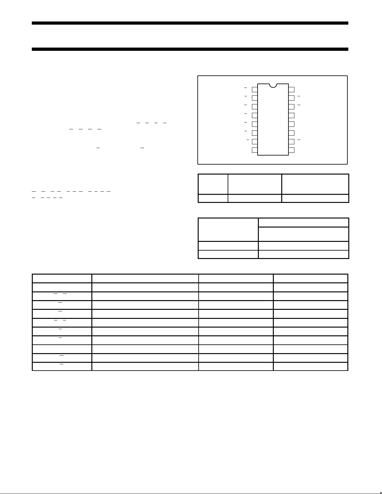
PIN CONFIGURATION
16
15
14
13
12
11
107
6
5
4
3
2
1
P
V
CC
Cn+x
Cn+y
G
Cn
P
2
G
2
G
1
P1
P
3
G
0
P
0
G3
98GND Cn+z
SF00725
TYPE
TYPICAL
PROPAGATION
DELAY
TYPICAL
SUPPLY CURRENT
(TOTAL)
74F182 5.0ns 21mA
ORDERING INFORMATION
ORDER CODE
DESCRIPTION
COMMERCIAL RANGE
V
CC
= 5V ±10%, T
amb
= 0°C to +70°C
16-pin plastic DIP N74F182N
16-pin plastic SO N74F182D
INPUT AND OUTPUT LOADING AND FAN-OUT TABLE
PINS DESCRIPTION 74FAST (U.L.) HIGH/LOW LOAD VALUE HIGH/LOW
Cn Carry input 2.5/2.0 50µA/1.2mA
G0, G2 Carry generate inputs (active-Low) 2.5/14.0 50µA/8.4mA
G1 Carry generate input (active-Low) 2.5/16.0 50µA/9.6mA
G3 Carry generate input (active-Low) 2.5/8.0 50µA/4.8mA
P0, P1 Carry propagate inputs (active-Low) 2.5/8.0 50µA/4.8mA
P2 Carry propagate input (active-Low) 2.5/6.0 50µA/3.6mA
P3 Carry propagate input (active-Low) 2.5/4.0 50µA/2.4mA
Cn+x–Cn+z Carry outputs 50/33 1.0mA/20mA
G Carry generate output (active-Low) 50/33 1.0mA/20mA
P Carry propagate output (active-Low) 50/33 1.0mA/20mA
NOTE:
One (1.0) FAST unit load is defined as: 20µA in the High state and 0.6mA in the Low state.
Page 2
Philips Semiconductors Product specification
74F182Look-ahead carry generator
1991 Apr 15
3
LOGIC SYMBOL
Cn+y Cn+zCn+x
P1 G1 P2 G2
2 1 15 14
12 11 9
VCC = Pin 16
GND = Pin 8
SF00726
G0
3P04
P36G3
5
10
7
13
G
P
Cn
IEC/IEEE SYMBOL
SF00727
CPG
13
4
14
6
5
12
11
9
7
10
C00
C01
C02
CP
CG
3
2
1
15
CI
CP0
CG0
CP1
CG1
CP2
CG2
CP3
CG3
LOGIC DIAGRAM
3
Cn
SF00724
4
13
1
2
14
15
5
6
G
0
P
0
G
1
P
1
G
2
P
2
G
3
P
3
12
11
9
10
7
G
P
Cn+z
Cn+y
Cn+x
V
CC
= Pin 16
GND = Pin 8
Page 3
Philips Semiconductors Product specification
74F182Look-ahead carry generator
1991 Apr 15
4
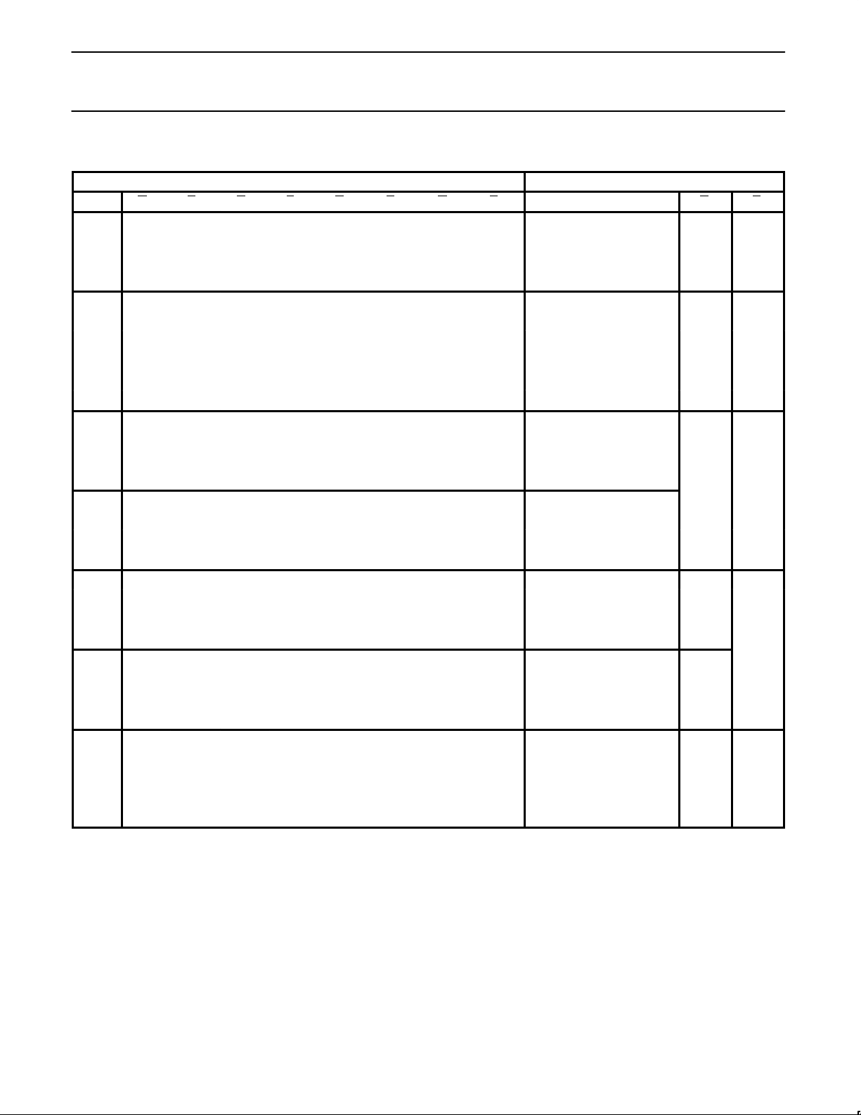
FUNCTION TABLE
INPUTS OUTPUTS
Cn G0 P0 G1 P1 G2 P2 G3 P3 Cn+x Cn+y Cn+z G P
X H H L
L H X L
X L X H
H X L H
X X X H H L
X H H H X L
L H X H X L
X X X L X H
X L X X L H
H X L X L H
X X X X X H H L
X X X H H H X L
X H H H X H X L
L H X H X H X L
X X X X X L X H
X X X L X X L H
X L X X L X L H
H X L X L X L H
X X X X X H H H
X X X H H H X H
X H H H X H X H
H H X H X H X H
X X X X X L X L
X X X L X X L L
X L X X L X L L
L X L X L X L L
H X X X H
X H X X H
X X H X H
X X X H H
L L L L L
NOTES:
H = High voltage level
L = Low voltage level
X = Don’t care
Page 4
Philips Semiconductors Product specification
74F182Look-ahead carry generator
1991 Apr 15
5
APPLICATION
SF00728
Cn+y Cn+zCn+x
P1 G1 P2 G2G0P0 P3 G3
G
P
Cn
Cn+y Cn+zCn+x
P1 G1 P2 G2G0P0 P3 G3
G
P
CnC
IN
Cn
Cn+4
G
P
ALU*
Cn
Cn+4
ALU*
Cn
Cn+4
ALU*
Cn
G
P
ALU*
Cn
Cn+4
G
P
ALU*
Cn
G
P
ALU*
Cn
G
P
ALU*
Cn
G
P
ALU*
74F182
74F182
COUT
(C32)
F
A, B
C18
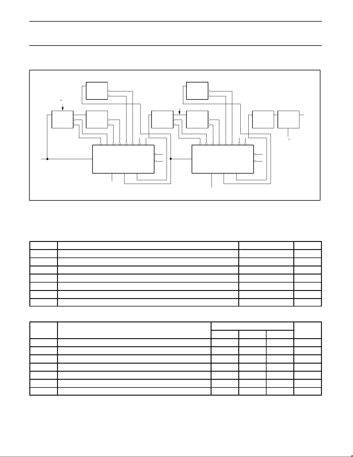
Figure 1. 32-Bit ALU with Ripple Carry Between 16-Bit Look-Ahead ALUs (*ALUs may be either 74F181 or 74F381)
ABSOLUTE MAXIMUM RATINGS
(Operation beyond the limit set forth in this table may impair the useful life of the device.
Unless otherwise noted these limits are over the operating free air temperature range.)
SYMBOL
PARAMETER RATING UNIT
V
CC
Supply voltage –0.5 to +7.0 V
V
IN
Input voltage –0.5 to +7.0 V
I
IN
Input current –30 to +5 mA
V
OUT
Voltage applied to output in High output state –0.5 to V
CC
V
I
OUT
Current applied to output in Low output state 40 mA
T
amb
Operating free-air temperature range 0 to +70 °C
T
stg
Storage temperature range –65 to +150 °C
RECOMMENDED OPERATING CONDITIONS
LIMITS
SYMBOL
PARAMETER
MIN NOM MAX
UNIT
V
CC
Supply voltage 4.5 5.0 5.5 V
V
IH
High-level input voltage 2.0 V
V
IL
Low-level input voltage 0.8 V
I
IK
Input clamp current –18 mA
I
OH
High-level output current –1 mA
I
OL
Low-level output current 20 mA
T
amb
Operating free-air temperature range 0 70 °C
Page 5
Philips Semiconductors Product specification
74F182Look-ahead carry generator
1991 Apr 15
6
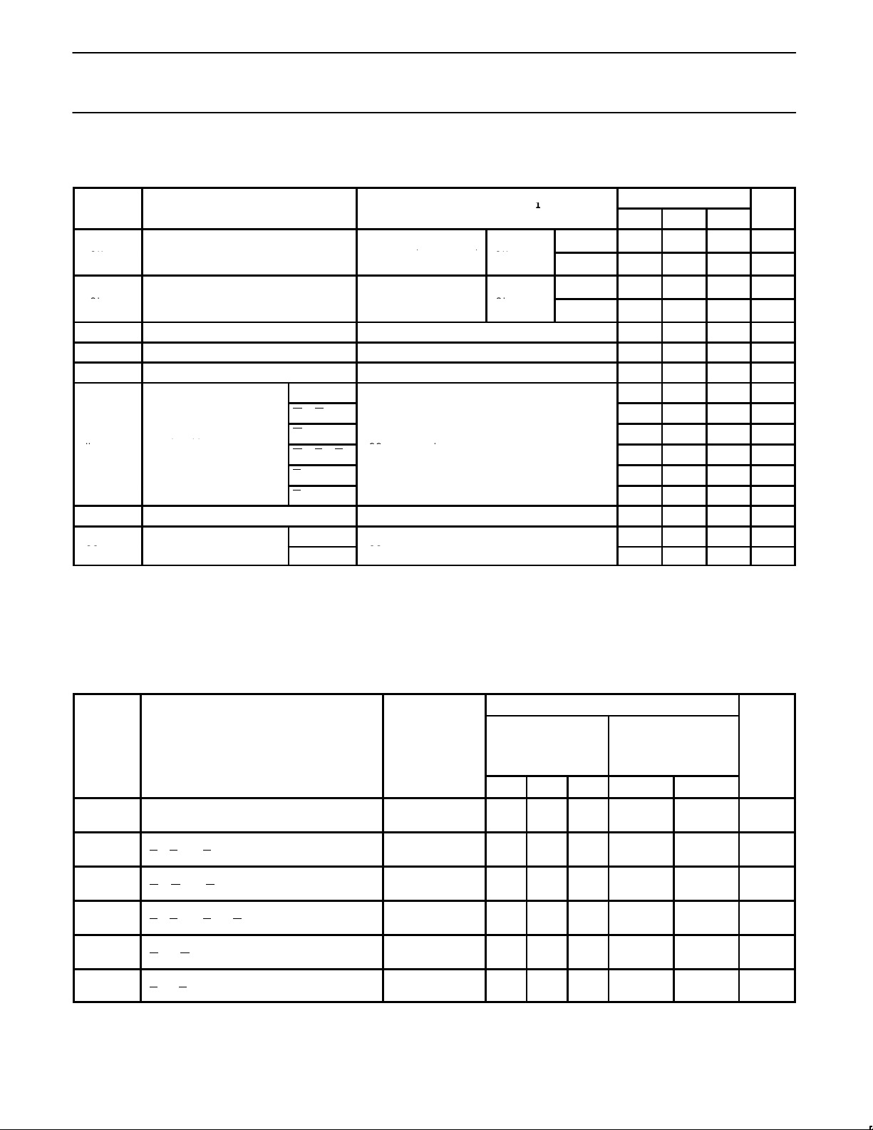
DC ELECTRICAL CHARACTERISTICS
(Over recommended operating free-air temperature range unless otherwise noted.)
LIMITS
SYMBOL
PARAMETER
TEST CONDITIONS
1
MIN TYP2MAX
UNIT
CC
= MIN, VIL = MAX,
±10%V
CC
2.5 V
VOHHigh-level output voltage
VCC = MIN, VIL = MAX,
V
IH
= MIN
I
OH
= MAX
±5%V
CC
2.7 3.4 V
CC
= MIN, VIL = MAX,
±10%V
CC
0.30 0.50 V
VOLLow-level output voltage
VCC = MIN, VIL = MAX,
VIH = MIN
I
OL
= MAX
±5%V
CC
0.30 0.50 V
V
IK
Input clamp voltage VCC = MIN, II = I
IK
–0.73 –1.2 V
I
I
Input current at maximum input voltage VCC = MAX, VI = 7.0V 250 µA
I
IH
High-level input current VCC = MAX, VI = 2.7V 250 µA
Cn
–1.2 mA
G0, G2
–8.4 mA
G1
–9.6 mA
IILLow-level input current
G3, P0, P1
VCC = MAX, VI = 0.5V
–4.8 mA
P2 –3.6 mA
P3 –2.4 mA
I
OS
Short-circuit output current
3
VCC = MAX –60 –150 mA
I
CCH
18 28 mA
ICCSupply current (total)
I
CCL
VCC = MAX
24 36 mA
NOTES:
1. For conditions shown as MIN or MAX, use the appropriate value specified under recommended operating conditions for the applicable type.
2. All typical values are at V
CC
= 5V, T
amb
= 25°C.
3. Not more than one output should be shorted at a time. For testing I
OS
, the use of high-speed test apparatus and/or sample-and-hold
techniques are preferable in order to minimize internal heating and more accurately reflect operational values. Otherwise, prolonged shorting
of a High output may raise the chip temperature well above normal and thereby cause invalid readings in other parameter tests. In any
sequence of parameter tests, I
OS
tests should be performed last.
AC ELECTRICAL CHARACTERISTICS
LIMITS
SYMBOL
PARAMETER
TEST
CONDITION
VCC = +5.0V
T
amb
= +25°C
CL = 50pF
RL = 500Ω
VCC = +5.0V ± 10%
T
amb
= 0°C to +70°C
CL = 50pF
RL = 500Ω
UNIT
MIN TYP MAX MIN MAX
t
PLH
t
PHL
Propagation delay
Cn to Cn+x, Cn+y, Cn+z
Waveform 2
2.5
2.5
5.0
5.0
8.0
7.5
2.5
2.5
8.5
8.5
ns
t
PLH
t
PHL
Propagation delay
P
0, P1, or P2 to Cn+x, Cn+y, Cn+z
Waveform 1
2.0
1.5
5.0
3.5
7.0
5.0
1.5
1.5
8.0
6.0
ns
t
PLH
t
PHL
Propagation delay
G
0, G1, or G2 to Cn+x, Cn+y , Cn+z
Waveform 1
1.5
1.5
4.0
3.0
7.5
5.0
1.5
1.5
8.5
5.5
ns
t
PLH
t
PHL
Propagation delay
P
1, P2, or P3 to G
Waveform 2
2.0
3.0
7.0
5.0
10.0
7.0
1.5
2.5
11.0
8.0
ns
t
PLH
t
PHL
Propagation delay
G
n to G
Waveform 2
1.5
3.0
5.0
5.0
7.0
7.0
1.5
2.5
7.5
8.0
ns
t
PLH
t
PHL
Propagation delay
P
n to P
Waveform 2
1.5
2.5
3.5
4.0
6.0
6.0
1.5
2.5
7.5
6.5
ns
V
V
Page 6
Philips Semiconductors Product specification
74F182Look-ahead carry generator
1991 Apr 15
7
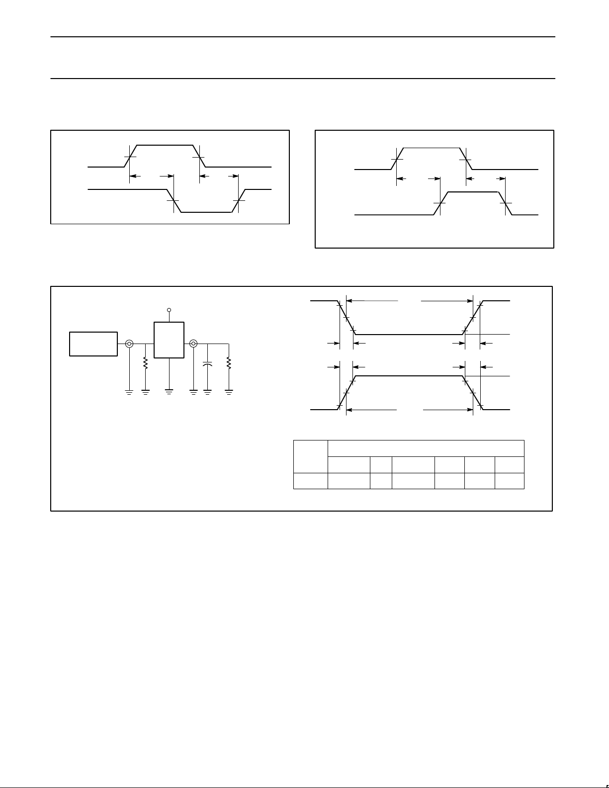
AC WAVEFORMS
For all waveforms, VM = 1.5V
V
M
V
M
V
M
V
M
V
OUT
V
IN
t
PHL
t
PLH
SF00093
Waveform 1. Propagation Delay for Inverting Outputs
V
M
V
M
V
M
V
M
V
OUT
V
IN
t
PLH
t
PHL
SF00092
Waveform 2. Propagation Delay for Non-Inverting Outputs
TEST CIRCUIT AND WAVEFORMS
t
w
90%
V
M
10%
90%
V
M
10%
90%
V
M
10%
90%
V
M
10%
NEGATIVE
PULSE
POSITIVE
PULSE
t
w
AMP (V)
0V
0V
t
THL (tf
)
INPUT PULSE REQUIREMENTS
rep. rate
t
w
t
TLHtTHL
1MHz 500ns
2.5ns 2.5ns
Input Pulse Definition
V
CC
family
74F
D.U.T.
PULSE
GENERATOR
R
L
C
L
R
T
V
IN
V
OUT
Test Circuit for Totem-Pole Outputs
DEFINITIONS:
R
L
= Load resistor;
see AC ELECTRICAL CHARACTERISTICS for value.
CL= Load capacitance includes jig and probe capacitance;
see AC ELECTRICAL CHARACTERISTICS for value.
R
T
= Termination resistance should be equal to Z
OUT
of
pulse generators.
t
THL (tf
)
t
TLH (tr
)
t
TLH (tr
)
AMP (V)
amplitude
3.0V
1.5V
V
M
SF00006
 Loading...