

Page 1
© 1999 Fairchild Semiconductor Corporation DS009491 www.fairchildsemi.com
April 1988
Revised July 1999
74F181 4-Bit Arithmetic Logic Unit
74F181
4-Bit Arithmetic Logic Unit
General Description
The 74F181 is a 4-bit Arithmetic logic Unit (ALU) which can
perform all the po ssible 16 logic operations on two variables and a variety of arithmetic operations. It is 40% faster
than the Schottky ALU and only consu mes 30% as much
power.
Features
■ Full lookahead for high-speed arithmetic operation on
long words
Ordering Code:
Devices also availab le in Tape and Reel. Specify by appending th e s uffix let t er “X” to the ordering code.
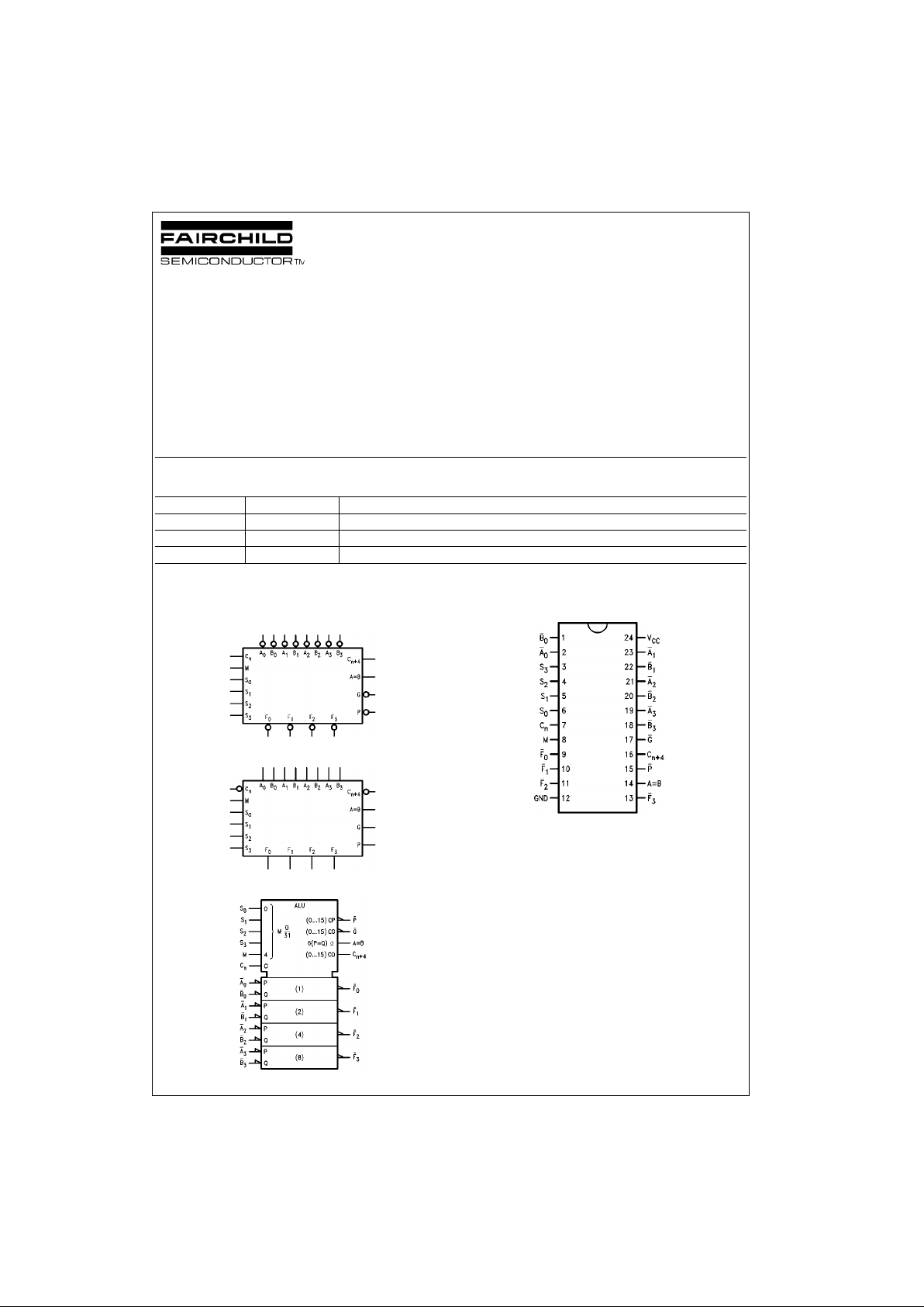
Logic Symbols
Active-HIGH Operands
Active-LOW Operands
IEEE/IEC
Connection Diagram
Order Number Package Number Package Description
74F181SC M24B 24-Lead Small Outline Integrated Circuit (SOIC), JEDEC MS-013, 0.300 Wide
74F181PC N24A 24-Lead Plastic Dual-In-Line Package (PDIP), JEDEC MS-010, 0.600 Wide
74F181SPC N24C 24-Lead Plastic Dual-In-Line Package (PDIP), JEDEC MS-100, 0.300 Wide
Page 2
www.fairchildsemi.com 2
74F181
Unit Loading/Fan Out
Note 1: OC-Open C ollector
Functional Description
The 74F181 is a 4-bit high-speed parallel Arithmetic Logic
Unit (ALU). Controlled by the four Function Select inputs
(S
0–S3
) and the Mode Control input (M), it can perform all
the 16 possible log ic operations or 16 different arithmetic
operations on Active HIGH or Active LOW operands. The
Function Table lists these operations.
When the Mode Control input (M) is HIGH, all internal carries are inhibited and the device p erforms l ogic oper ations
on the individual bits as listed. When the Mode Control
input is LOW, the carries are enabled and the dev ice performs arithmetic operations on the two 4-bit words. The
device incorporates full internal carry l ookahead and provides for either ripple carry between devices using the
C
n + 4
output, or for carry lookahead between packages
using the signals P
(Carry Propagate) and G (Carry Gener-
ate). In the Add mode, P
indicates that F is 15 or more,
while G
indicates that F is 16 or more. In the Subtract mode
P
indicates that F is zero or less, while G indicates that F is
less than zero. P
and G are not affected by carry in. When
speed requiremen ts are not stringent , the 74F181 can be
used in a simple Ripple Carry mode by connecting the
Carry output (C
n
+4) signal to the Carry input (Cn) of the
next unit. For h igh speed operation t he device is used in
conjunction with a carry lookahead circuit. One carry lookahead package is requ ired for each group of four 74F181
devices. Carry lookahead can be provided at various levels
and offers high speed capability over extremely long wo rd
lengths.
The A = B output from the device goes HIGH w hen all four
F
outputs are HIGH and can be used to indicate logic
equivalence over four bits when the u nit is in t he Subtract
mode. The A = B output is open collector and can be wired
AND with other A = B outputs to give a comparison for
more than four bits. The A = B signal can also be used with
the C
n+4
signal to indicate A > B and A < B.
The Function Table lists the arithmetic ope rations that are
performed without a carry in. An incoming carry adds a one
to each operation . Thus, select code LHHL gene rates A
minus B minus 1 (2s complem ent no tation) witho ut a ca rry
in and generates A minus B when a carry is applied.
Because subtraction is actual ly performed by co mplementary addition (1s complement), a carry out means borrow
;
thus a carry is gener ated when there is no underflow a nd
no carry is generated when there is underflow. As indicated, this device can be used with either active LOW
inputs producing active LOW outputs or with active HIGH
inputs producing active HIGH outp uts. For either case the
table lists the operatio ns that are performed to the operands labeled inside the logic symbol.
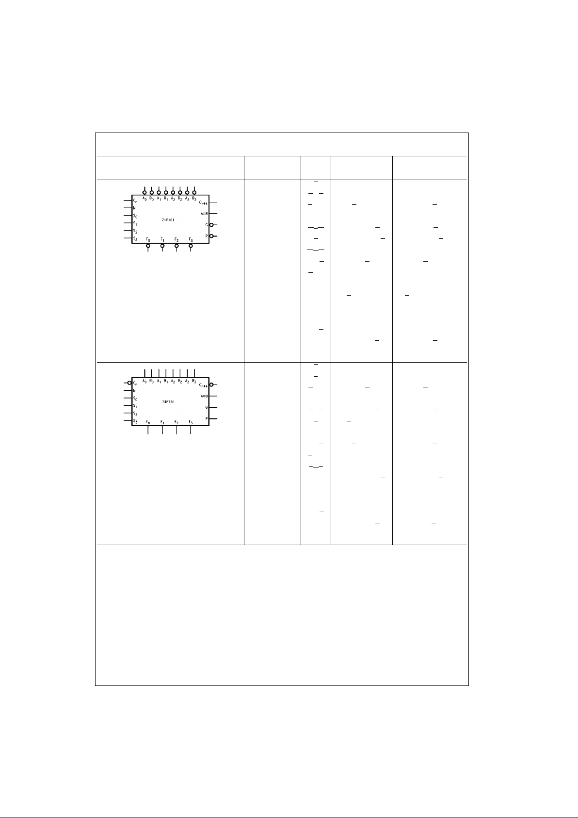
Pin Names Description
U.L.
Input I
IH/IIL
HIGH/LOW
Output I
OH/IOL
A0–A
3
A Operand Inputs (Active LOW) 1.0/3.0 20 µA/−1.8 mA
B
0–B3
B Operand Inputs (Active LOW) 1.0/3.0 20 µA/−1.8 mA
S
0–S3
Function Select Inputs 1.0/4.0 20 µA/−2.4 mA
M Mode Control Input 1.0/1.0 20 µA/−0.6 mA
C
n
Carry Input 1.0/5.0 20 µA/−3.0 mA
F
0–F3
Function Outputs (Active LOW) 50/33.3 −1 mA/20 mA
A = B Comparator Output OC (Note 1)/33.3 (Note 1)/20 mA
G
Carry Generate Output (Active LOW) 50/33.3 −1 mA/20 mA
P
Carry Propagate Output (Active LOW) 50/33.3 −1 mA/20 mA
C
n + 4
Carry Output 50/33.3 −1 mA/20 mA
Page 3
3 www.fairchildsemi.com
74F181
Operation Table
Logic Arithmetic Arithmetic
S
0S1S2S3
(M=H) (M=L, C0=Inactive) (M=L, C0=Active)
a. All Input Data Inverted
LLLL A
A minus 1 A
HLLL A
• B A • B minus 1 A • B
LHLL A
+ BA • B minus 1 A • B
H H L L Logic “1” minus 1 (2s comp.) Zero
LLHL A
+ B A plus (A + B) A plus (A + B) plus 1
HLHL B
A • B plus (A + B) A • B plus (A + B) plus 1
LHHLA
⊕ B A minus B minus 1 A minus B
HHHL A + B
A + B A + B plus 1
LLLHA
• B A plus (A + B) A plus (A + B plus 1
HLLH A⊕B A plus B A plus B plus 1
LHLH B A • B
plus (A + B) A • B plus (A + B) plus 1
HHLH A + BA + BA + B plus 1
L L H H Logic “0” A plus A (2 × A) A plus A (2 × A) plus 1
HLHH A • B
A plus A • B A plus A • B plus 1
L H H H A • B A plus A • B
A plus A • B plus 1
HHHH A A A plus 1
b. All Input Data True
LLLL A
A A plus 1
HLLLA
+ B A + BA + B plus 1
LHLL A
• B A + B A + B plus 1
H H L L Logic “0” minus 1 (2s comp.) Zero
LLHL A
• B A plus (A • B)A plus A • B plus 1
HLHL B
A • B plus (A + B) A • B plus (A + B) plus 1
LHHLA ⊕ B A minus B minus 1 A minus B
HHHL A • B
A • B minus 1 A • B
LLLHA + B A plus A • B A plus A • B plus 1
HLLH A
⊕B A plus B A plus B plus 1
LHLH B A • B plus (A + B
) A • B plus (A + B) plus 1
H H L H A • B A • B minus 1 A • B
L L H H Logic “1” A plus A (2 × A) A plus A (2 × A) plus 1
HLHHA + B
A plus (A + B) A plus (A+B) plus 1
LHHH A + B A plus (A + B
)A plus (A+B) plus 1
HHHH A A minus 1 A
Page 4

www.fairchildsemi.com 4
74F181
Logic Arithmetic Arithmetic
S
0S1S2S3
(M=H) (M=L, C0=Inactive) (M=L, C0=Active)
c. A All Input Data Inverted; B Input Data True
LLLL A
A minus 1 A
HLLLA
+ B A • B minus 1 A • B
LHLL A
• B A • B minus 1 A • B
H H L L Logic “1” minus 1 (2s comp.) Zero
LLHL A
• B A plus (A + B) A plus (A + B) plus 1
HLHL B A • B
plus (A + B) A • B plus (A + B) plus 1
LHHL A ⊕ B A plus B A plus B plus 1
HHHL A + BA + BA + B plus 1
LLLHA
+ B A plus (A + B) A plus (A + B) plus 1
HLLH A
⊕B A minus B minus 1 A minus B
LHLH B
A • B plus (A + B)A • B plus (A + B) plus 1
HHLH A + B
A + B A + B plus 1
L L H H Logic “0” A plus A (2 × A) A plus A (2 × A) plus 1
H L H H A • B A plus A • B
A plus A • B plus 1
LHHH A • B
A plus A • B A plus A • B plus 1
HHHH A A A plus 1
d. A Input Data True; B Input Date Inverted
LLLL A
A A plus 1
HLLL A
• B A + B A + B plus 1
LHLL A
+ B A + BA + B plus 1
H H L L Logic “0” minus 1 (2s comp.) Zero
LLHL A
+ B A plus A • B A plus A • B plus 1
HLHL B A • B plus (A + B
)A • B plus (A + B) plus 1
LHHL A
⊕ B A plus B A plus B plus 1
H H H L A • B A • B minus 1 A • B
LLLH A
• B A plus A • B A plus A • B plus 1
HLLH A⊕B A minus B minus 1 A minus B
LHLH B
A • B plus (A + B) A • B plus (A + B) plus 1
HHLH A • B
A • B minus 1 A • B
L L H H Logic “1” A plus A (2 × A) A plus A (2 × A) plus 1
HLHH A + BA plus (A + B
) A plus (A+B) plus 1
LHHH A + B
A plus (A + B) A plus (A+B) plus 1
HHHH A A minus 1 A
Page 5

5 www.fairchildsemi.com
74F181
Logic Diagram
Please note that this d iagram is provided only f or t he understanding of lo gic operations and should not be used to estimat e propagation delays.
p
Page 6

www.fairchildsemi.com 6
74F181
Absolute Maximum Ratings(Note 2) Recommended Operating
Conditions
Note 2: Absolute maximum ratings are values beyond which the device
may be damaged or have its useful life impaired. Functional operation
under these conditi ons is not implied.
Note 3: Either voltage limit or curren t limit is sufficient to protect in put s .
DC Electrical Characteristics
Storage Temperature −65°C to +150°C
Ambient Temperature under Bias −55°C to +125°C
Junction Temperature under Bias −55°C to +150°C
V
CC
Pin Potential to Ground Pin −0.5V to +7.0V
Input Voltage (Note 3) −0.5V to +7.0V
Input Current (Note 3) −30 mA to +5.0 mA
Voltage Applied to Output
in HIGH State (with V
CC
= 0V)
Standard Output −0.5V to V
CC
3-STATE Output −0.5V to +5.5V
Current Applied to Output
in LOW State (Max) twice the rated I
OL
(mA)
ESD Last Passing Voltage (Min) 4000V
Free Air Ambient Temperature 0°C to +70°C
Supply Voltage +4.5V to +5.5V
Symbol Parameter Min Typ Max Units
V
CC
Conditions
V
IH
Input HIGH Voltage 2.0 V Recognized as a HIGH Signal
V
IL
Input LOW Voltage 0.8 V Recognized as a LOW Signal
V
CD
Input Clamp Diode Voltage −1.2 V Min IIN = −18 mA
V
OH
Output HIGH 10% V
CC
2.5
VMin
IOH = −1 mA
Voltage 5% V
CC
2.7 IOH = −1 mA
V
OL
Output LOW 10% V
CC
0.5 V Min IOL = 20 mA
Voltage
I
IH
Input HIGH
5.0 µAMaxVIN = 2.7V
Current
I
BVI
Input HIGH Current
7.0 µAMaxVIN = 7.0V
Breakdown Test
I
CEX
Output HIGH
50 µAMaxV
OUT
= VCC (Fn, G, P, C
n+4
)
Leakage Current
V
ID
Input Leakage
4.75 V 0.0
IID = 1.9 µA
Test All Other Pins Grounded
I
OD
Output Leakage
3.75 µA0.0
V
IOD
= 150 mV
Circuit Current All Other Pins Grounded
I
IL
Input LOW Current −0.6
mA Max
VIN = 0.5V (M)
−1.8
VIN = 0.5V (A0, A1, A3, B0, B1, B3)
−2.4
VIN = 0.5V (Sn, A2, B2)
−3.0
VIN = 0.5V (Cn)
I
OS
Output Short-Circuit Current −60 −150 mA Max V
OUT
= 0V (Fn, G, P, C
n+4
)
I
OHC
Open Collector, Output
250 µAMinVO = VCC (A = B)
OFF Leakage Test
I
CCH
Power Supply Current 43 65.0 mA Max VO = HIGH
I
CCL
Power Supply Current 43 65.0 mA Max VO = LOW
Page 7

7 www.fairchildsemi.com
74F181
AC Electrical Characteristics
TA = +25°CT
A
= −55°C to +125°CTA = 0°C to +70°C
Symbol Parameter VCC = +5.0V VCC = +5.0V VCC = +5.0V Units
CL = 50 pF CL = 50 pF CL = 50 pF
Path Mode Min Typ Max Min Max Min Max
t
PLH
Propagation Delay 3.0 6.4 8.5 3.0 10.0 3.0 9.5
ns
t
PHL
Cn to C
n + 4
3.0 6.1 8.0 3.0 9.5 3.0 9.0
t
PLH
Propagation Delay 5.0 10.0 13.0 5.0 15.5 5.0 14.0
ns
t
PHL
A or B to C
n + 4
Sum4.0 9.412.03.516.54.013.0
t
PLH
Propagation Delay 5.0 10.8 14.0 5.0 17.0 5.0 15.0
ns
t
PHL
A or B to C
n + 4
Dif 5.0 10.0 13.0 4.0 15.0 5.0 14.0
t
PLH
Propagation Delay 3.0 6.7 8.5 2.5 16.0 3.0 9.5
ns
t
PHL
Cn to F
Any 3.0 6.5 8.5 2.5 12.0 3.0 9.5
t
PLH
Propagation Delay 3.0 5.7 7.5 2.5 9.0 3.0 8.5
ns
t
PHL
A or B or G
Sum 3.0 5.8 7.5 2.5 9.5 3.0 8.5
t
PLH
Propagation Delay 3.0 6.5 8.5 2.5 11.5 3.0 9.5
ns
t
PHL
A or B to G
Dif 3.0 7 .3 9.5 2.5 11.0 3.0 10.5
t
PLH
Propagation Delay 3.0 5.0 7.0 2.5 8.5 3.0 8.0
ns
t
PHL
A or B to P
Sum 3.0 5.5 7.5 3.0 9.5 3.0 8.5
t
PLH
Propagation Delay 3.0 5.8 7.5 2.5 11.0 3.0 8.5
ns
t
PHL
A or B to P
Dif 4.0 6.5 8.5 3.0 11.0 4.0 9.5
t
PLH
Propagation Delay 3.0 7.0 9.0 3.0 14.5 3.0 10.0
ns
t
PHL
Ai or Bi to F
i
Sum3.0 7.210.03.014.53.010.0
t
PLH
Propagation Delay 3.0 8.2 11.0 3.0 17.5 3.0 12.0
ns
t
PHL
Ai or Bi to F
i
Dif 3.0 5 .0 11.0 3.0 14.5 3.0 12.0
t
PLH
Propagation Delay 4.0 8.0 10.5 3.5 16.5 4.0 11.5
ns
t
PHL
Any A or B to Any F
Sum4.0 7.810.04.013.54.011.0
t
PLH
Propagation Delay 4.5 9.4 12.0 3.5 17.5 4.5 13.0
ns
t
PHL
Any A or B to Any F
Dif 3.5 9 .4 12.0 3.0 14.0 3.5 13.0
t
PLH
Propagation Delay 4.0 6.0 9.0 3.5 14.5 4.0 10.0
ns
t
PHL
A or B to F
Logic 4.0 6.0 10.0 3.0 15.5 4.0 11.0
t
PLH
Propagation Delay 11.0 18.5 27.0 8.0 35.0 11.0 29.0
ns
t
PHL
A or B to A = B
Dif 6.0 9 .8 12.5 5.5 21.0 6.0 13.5
Page 8

www.fairchildsemi.com 8
74F181
Physical Dimensions inches (millimeters) unless otherwise noted
24-Lead Small Outline Integrated Circuit (SOIC), JEDEC MS-013, 0.300 Wide
Package Number M24B
24-Lead Plastic Dual-In-Line Package (PDIP), JEDEC MS-010, 0.600 Wide
Package Number N24A
Page 9

9 www.fairchildsemi.com
74F181 4-Bit Arithmetic Logic Unit
Physical Dimensions inches (millimeters) unless otherwise noted (Continued)
24-Lead Plastic Dual-In-Line Package (PDIP), JEDEC MS-100, 0.300 Wide
Package Number N24C
Fairchild does not assume any responsibility for use of any circu itry described, no circuit patent license s are implied and
Fairchild reserves the right at any time without notice to change said circuitry and specifications.
LIFE SUPPORT POLICY
FAIRCHILD’S PRODUCTS ARE NOT AUTHORIZED FOR USE AS CRITICAL COMPONENTS IN LIFE SUPPORT
DEVICES OR SYSTEMS WITHOUT THE EXPRESS WRITTEN APPROVAL OF THE PRESIDENT OF FAIRCHILD
SEMICONDUCTOR CORPORATION. As used herein:
1. Life sup por t de vices o r syst ems are dev ic es or syste ms
which, (a) are intended for surgical implant into the
body, or (b) support or sustain life, and (c) whose failure
to perform when properly used in accordance with
instructions for use provided i n the labe li ng, can be re asonably expected to result in a significant injury to the
user.
2. A c ritical compo nent in any com ponen t of a life s uppor t
device or system whose failu re to perform can b e reasonably expected to c ause th e fa i lure of the li fe s upp or t
device or system, or to affect its safety or effectiveness.
www.fairchildsemi.com
 Loading...