

Page 1

INTEGRATED CIRCUITS
74ALVCHS162830
18-bit to 36-bit address driver
with bus hold (3-State)
Product data 2001 Sep 07
File under Integrated Circuits — ICL03
Page 2
Philips Semiconductors Product data
74ALVCHS16283018-bit to 36-bit address driver with bus hold (3-State)
FEA TURES
•Output ports have equivalent 26 Ω series resistors, so no external
resistors are required
•Diodes on inputs clamp overshoot
•ESD classification testing is done to JEDEC Standard JESD22.
Protection exceeds 2000 V HBM per method A114.
•Latch-up testing is done to JEDEC Standard JESD78, which
exceeds 100 mA.
•Bus hold on data inputs eliminates the need for external
pullup/pulldown resistors
•Packaged in thin very small-outline package (TVSOP) — 0.4 mm
pitch
•Optimized for use with PCK953 in SDRAM module applications
•Balanced ±12 mA output drive
•Low noise, low skew
DESCRIPTION
The ALVCHS162830 address driver is designed for 2.3 V to 3.6 V
V
operation.
CC
Diodes to VCC have been added on the inputs to clamp overshoot.
The bus hold feature retains the inputs’ last state whenever the input
bus goes to high impedance. This prevents floating inputs and
eliminates the need for pull up or pull down resistors.
The outputs, which are designed to sink up to 12 mA, include
equivalent 26 Ω series resistors to reduce overshoot and
undershoot.
To ensure the high-impedance state during power up or power
down, the output-enable (OE
pullup resistor; the minimum value of the resistor is determined by
the current-sinking capability of the driver.
The 74ALVCHS162830 is characterized for operation from –40 to
+85 °C.
FUNCTION TABLE
Inputs Outputs
OE1 OE2 A 1Yn 2Yn
L H H H Z
L H L L Z
H L H Z H
H L L Z L
L L H H H
L L L L L
H H X Z Z
) input should be tied to VCC through a
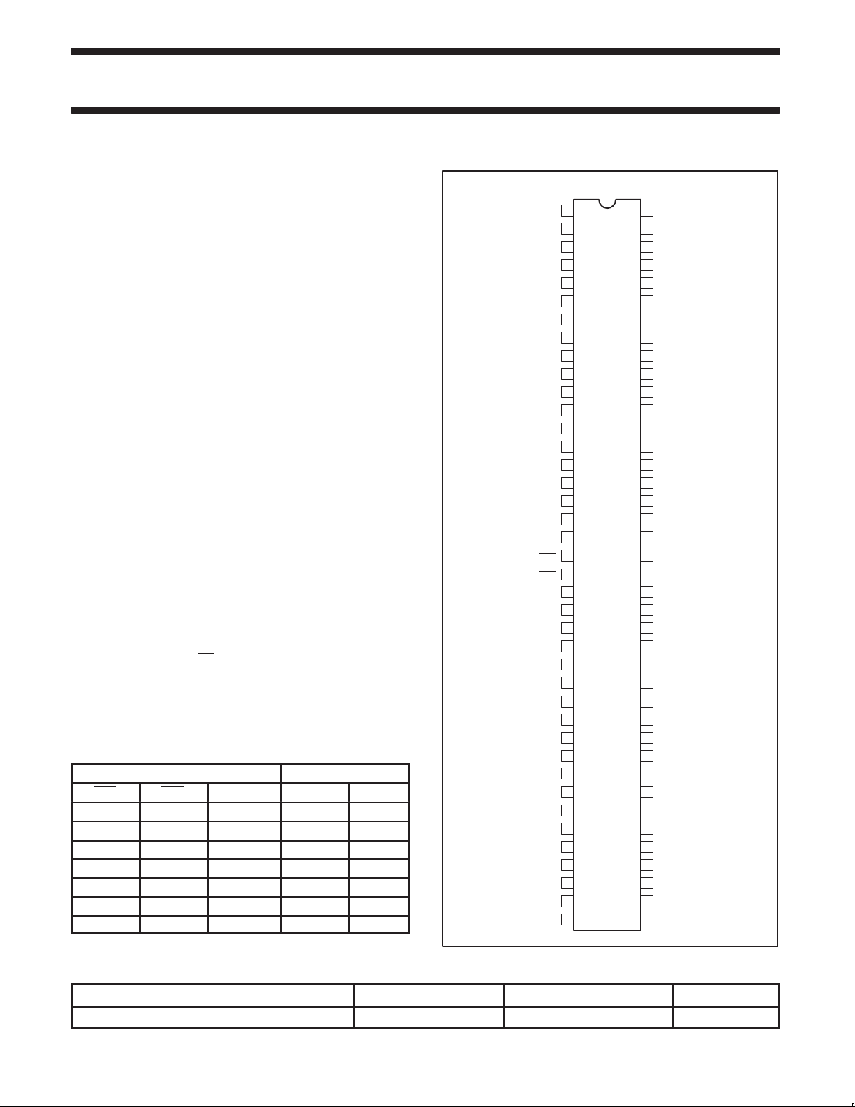
PIN CONFIGURA TION
2Y2
1
2
1Y2
3
GND
4
2Y1
5
1Y1
6
V
CC
7
A1
8
A2
9
GND
10
A3
11
A4
12 69
GND
13
A5
14
A6
15
V
CC
16
A7
17
A8
18 63
GND
19 62
A9
20
OE1
21
OE2
22
A10
23
GND
24
A11
25 56
A12
26 55
V
CC
A13
27 54
28
A14
GND
29
30
A15
31
A16
32 49
GND
33 48
A17
34 47
A18
V
35 46
CC
36
2Y18
1Y18
37
38
GND
39
2Y17
40 41
1Y17
TOP VIEW
1Y3
80
79
2Y3
78
GND
77
1Y4
76
2Y4
75
V
CC
74
1Y5
2Y5
73
72
GND
71
1Y6
70
2Y6
GND
68
1Y7
2Y7
67
66
V
CC
1Y8
65
64
2Y8
GND
1Y9
61
2Y9
60
1Y10
59
2Y10
58
GND
57
1Y11
2Y11
V
CC
1Y12
53
2Y12
52
GND
51
1Y13
50
2Y13
GND
1Y14
2Y14
V
CC
45
1Y15
2Y15
44
GND
43
42
1Y16
2Y16
SW00723
ORDERING INFORMATION
PACKAGES TEMPERATURE RANGE ORDER CODE DWG NUMBER
80-pin plastic thin very small outline (TVSOP) –40 to +85 °C 74ALVCHS162830DGB SOT647-1
2001 Sep 07 853-2279 27052
2
Page 3
Philips Semiconductors Product data
18-bit to 36-bit address driver with bus hold
(3-State)
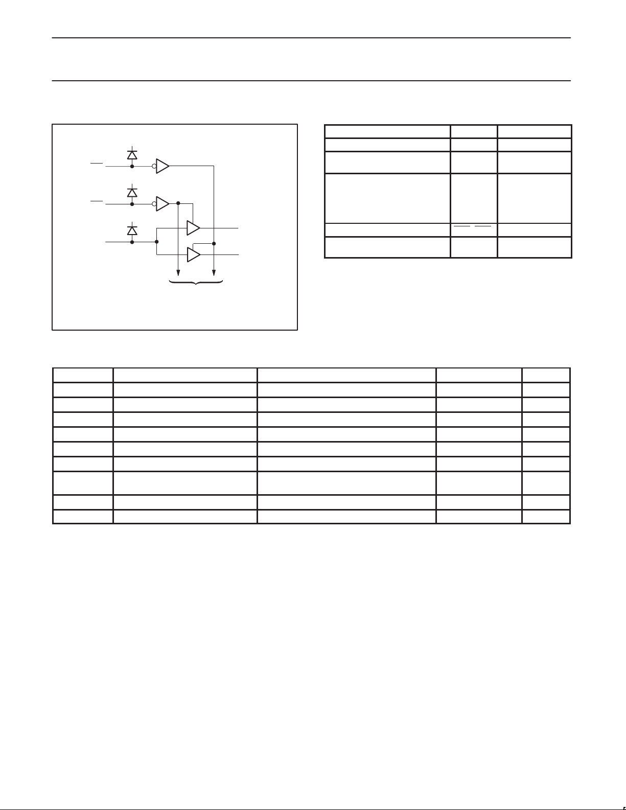
LOGIC DIAGRAM (POSITIVE LOGIC)
V
CC
21
OE2
V
CC
20
OE1
V
CC
7
A1
to 17 other channels
5
1Y1
4
2Y1
SW00724
74ALVCHS162830
PIN DESCRIPTION
PIN(S) SYMBOL FUNCTION
6, 15, 26, 35, 46, 55, 66, 75 V
7, 8, 10, 11, 13, 14, 16, 17, 19,
22, 24, 25, 27, 28, 30, 31, 33, 34
1, 2, 4, 5, 36, 37, 39, 40, 41, 42,
CC
An Inputs
1Yn, 2Yn Outputs
44, 45, 47, 48, 50, 51, 53, 54,
56, 57, 59, 60, 61, 62, 64, 65,
67, 68, 70, 71, 73, 74, 76, 77,
79, 80
20, 21 OE1, OE2 Output enable
3, 9, 12, 18, 23, 29, 32, 38, 43,
49, 52, 58, 63, 69, 72, 78
GND Ground
Supply voltage
ABSOLUTE MAXIMUM RATINGS
Over recommended operating free-air temperature range (unless otherwise noted).
SYMBOL PARAMETER CONDITIONS RATING UNIT
V
ICC, I
Θ
T
CC
V
I
V
O
I
IK
I
OK
I
O
GND
JA
stg
Supply voltage range –0.5 to +4.6 V
Input voltage range See Note 2 –0.5 to +4.6 V
Output voltage range See Notes 2 and 3 –0.5 to VCC +0.5 V
Input clamp current VI < 0 –50 mA
Output clamp current VO < 0 –50 mA
Continuous output current "50 mA
Continuous current through each V
or GND
CC
Package thermal impedance See Note 4 106 °C/W
Storage temperature range –65 to +150 °C
NOTES:
1. Stresses beyond those listed under ”absolute maximum ratings” may cause permanent damage to the device. These are stress ratings
only, and functional operation of the device at these or any other conditions beyond those indicated under ”recommended operating
conditions” is not implied. Exposure to absolute-maximum-rated conditions for extended periods may affect device reliability .
2. The input negative-voltage and output voltage ratings may be exceeded if the input and output current ratings are observed.
3. This value is limited to 4.6 V maximum.
4. The package thermal impedance is calculated in accordance with JESD 51.
1
"100 mA
2001 Sep 07
3
Page 4
Philips Semiconductors Product data
SYMBOL
PARAMETER
CONDITIONS
UNIT
V
High-level input voltage
V
V
Low-level input voltage
V
18-bit to 36-bit address driver with bus hold
(3-State)
RECOMMENDED OPERATING CONDITIONS
All unused control inputs of the device must be held at VCC or GND to ensure proper device operation.
V
CC
IH
IL
V
V
O
I
OH
I
OL
∆t/∆v Input transition rise or fall rate 10 ns/V
T
amb
Supply voltage 2.3 3.6 V
p
p
Input voltage 0 V
I
Output voltage 0 V
High-level output current
Low-level output current
Operating free-air temperature –40 +85 °C
VCC = 2.3 V to 2.7 V 1.7
VCC = 2.7 V to 3.6 V 2
VCC = 2.3 V to 2.7 V 0.7
VCC = 2.7 V to 3.6 V 0.8
VCC = 2.3 V –6
VCC = 2.7 V –8
VCC = 3 V –12
VCC = 2.3 V 6
VCC = 2.7 V 8
VCC = 3 V 12
74ALVCHS162830
LIMITS
MIN MAX
CC
CC
V
V
mA
mA
2001 Sep 07
4
Page 5

Philips Semiconductors Product data
V
V
O
OH
I
mA
O
OL
I
mA
C
V
V
GND
3.3 V
pF
18-bit to 36-bit address driver with bus hold
(3-State)
ELECTRICAL CHARACTERISTICS
Over recommended operating free-air temperature range (unless otherwise noted).
SYMBOL PARAMETER TEST CONDITIONS V
II = –18 mA 2.3 V –1.2
IK
II = 18 mA 2.3 V VCC+1.2
IOH = –100 µA
IOH = –4 mA, VIH = 1.7 V 2.3 V 1.9
V
H
OH
= –6
VIH = 1.7 V 2.3 V 1.7
VIH = 2 V 3 V 2.4
IOH = –8 mA, VIH = 2 V 2.7 V 2
IOH = –12 mA, VIH = 2 V 3 V 2
IOL = 100 µA
IOL = 4 mA, VIL = 0.7 V 2.3 V 0.4
V
L
OL
= 6
VIL = 0.7 V 2.3 V 0.55
VIL = 0.8 V 3 V 0.55
IOL = 8 mA, VIL = 0.8 V 2.7 V 0.6
IOL = 12 mA, VIL = 0.8 V 3 V 0.8
I
I
V
= VCC or GND 3.6 V ±5 µA
I
VI = 0.7 V 2.3 V 45
VI = 1.7 V 2.3 V –45
I
I(hold)
VI = 0.8 V 3 V 75
VI = 2 V 3 V –75
CC
2
or
VI = 0 to 3.6 V
I
OZ
I
CC
∆I
CC
Control inputs
i
Data inputs
C
Outputs VO = VCC or GND 3.3 V 3.12 pF
o
VO = VCC or GND 3.6 V ±10 µA
VI = VCC or GND, IO = 0 3.6 V 40 µA
One input at VCC – 0.6 V,
Other inputs at VCC or GND
=
I
NOTES:
1. All typical values are at V
2. This is the bus-hold maximum dynamic current. It is the minimum overdrive current required to switch the input from one state to another.
= 3.3 V, T
CC
amb
= 25°C.
CC
2.3 V to
3.6 V
2.3 V to
3.6 V
3.6 V ±500
3 V to
3.6 V
74ALVCHS162830
LIMITS
3.5
7.64
1
MAX UNIT
0.2
750 µA
MIN TYP
VCC–0.2
µA
p
V
V
2001 Sep 07
5
Page 6

Philips Semiconductors Product data
PARAMETER
UNIT
SYMBOL
PARAMETER
TEST CONDITIONS
UNIT
C
C
pF
18-bit to 36-bit address driver with bus hold
(3-State)
SWITCHING CHARACTERISTICS
Over recommended operating free-air temperature range (unless otherwise noted) (see Figures 1 and 2).
FROM TO
(INPUT) (OUTPUT)
t
pd
t
en
t
dis
1
t
sk(o)
NOTE:
1. Output skew between any 2 outputs of same part switching in the same direction.
OPERATING CHARACTERISTICS, T
pd
A Y 1.2 3.8 4 1.7 3.5 ns
OE Y 1 5.7 5.7 1 4.8 ns
OE Y 1 4.9 5.4 1.7 5.2 ns
Output skew – – – – – – 500 ps
amb
Power dissipation
p
capacitance per
driver
p
All outputs enabled
All outputs disabled
VCC = 2.5 V ± 0.2 V VCC = 2.7 V VCC = 3.3 V ± 0.3 V
MIN MAX MIN MAX MIN MAX
= 25°C
VCC = 2.5 V ± 0.2 V VCC = 3.3 V ± 0.3 V
TYP TYP
= 0, f = 10 MHz
L
49 53
6 7.5
74ALVCHS162830
p
2001 Sep 07
6
Page 7

Philips Semiconductors Product data
18-bit to 36-bit address driver with bus hold
(3-State)
From Output
Under Test
C
= 30 pF
L
(see Note A)
Timing
Input
Data
Input
500 Ω
Load Circuit
VCC/2
t
su
PARAMETER MEASUREMENT INFORMATION
500 Ω
t
h
VCC/2VCC/2
VCC = 2.5 V ± 0.2 V
2 × V
S1
Open
GND
V
CC
0 V
V
CC
0 V
CC
Input
74ALVCHS162830
TEST S
t
pd
t
PLZ/tPZL
t
PHZ/tPZH
Voltage Waveforms
Pulse Duration
t
w
Open
2 × V
GND
1
CC
V
VCC/2VCC/2
CC
0 V
Voltage Waveforms
Input
Output
Setup and Hold Times
VCC/2 VCC/2
t
PLH
VCC/2 VCC/2
Voltage Waveforms
Propagation Delay Times
V
CC
0 V
t
PHL
V
OH
V
OL
Output
Control
(low-level
enabling)
Output
Waveform 1
S1 at 2 x V
(see Note B)
Output
Waveform 2
S1 at GND
(see Note B)
/2
VCC/2
t
PZL
CC
t
PZH
VCC/2
VCC/2
V
CC
t
PLZ
V
+ 0.15 V
OL
t
PHZ
V
– 0.15 V
OH
Voltage Waveforms
Enable and Disable Times
NOTES:
A. CL includes probe and jig capacitance.
B. Waveform 1 is for an output with internal conditions such that the output is low except when disabled by the output control.
Waveform 2 is for an output with internal conditions such that the output is high except when disabled by the output control.
C. All input pulses are supplied by generators having the following characteristics: PRR ≤ 10 MHz, Z
= 50 Ω, tr ≤ 2 ns, tf ≤ 2 ns.
O
D. The outputs are measured one at a time with one transition per measurement.
E. t
F. t
G. t
PLZ
PZL
PLH
and t
and t
and t
are the same as t
PHZ
are the same as ten.
PZH
are the same as tpd.
PHL
dis
.
Figure 1. Load circuit and voltage waveforms
V
0 V
V
0 V
V
V
CC
CC
OL
OH
SV01849
2001 Sep 07
7
Page 8

Philips Semiconductors Product data
18-bit to 36-bit address driver with bus hold
(3-State)
From Output
Under Test
C
= 50 pF
L
(see Note A)
Timing
Input
Data
Input
500 Ω
Load Circuit
1.5 V
t
su
PARAMETER MEASUREMENT INFORMATION
500 Ω
t
h
VCC = 2.7 V and 3.3 V ± 0.3 V
6 V
S1
Open
GND
2.7 V
0 V
1.5 V1.5 V
2.7 V
0 V
Input
74ALVCHS162830
TEST S
t
pd
t
PLZ/tPZL
t
PHZ/tPZH
Voltage Waveforms
Pulse Duration
t
1
Open
6 V
GND
w
1.5 V1.5 V
2.7 V
0 V
Voltage Waveforms
Input
Output
Setup and Hold Times
1.5 V 1.5 V
t
PLH
1.5 V 1.5 V
Voltage Waveforms
Propagation Delay Times
2.7 V
0 V
t
PHL
V
OH
V
OL
Output
Control
(low-level
enabling)
Output
Waveform 1
S1 at 6 V
(see Note B)
Output
Waveform 2
S1 at GND
(see Note B)
1.5 V
t
PZL
1.5 V
t
PZH
1.5 V
Voltage Waveforms
Enable and Disable Times
1.5 V
V
V
OL
OH
t
PLZ
+ 0.3 V
t
PHZ
– 0.3 V
NOTES:
A. CL includes probe and jig capacitance.
B. Waveform 1 is for an output with internal conditions such that the output is low except when disabled by the output control.
Waveform 2 is for an output with internal conditions such that the output is high except when disabled by the output control.
C. All input pulses are supplied by generators having the following characteristics: PRR ≤ 10 MHz, Z
= 50 Ω, tr ≤ 2.5 ns, tf ≤ 2.5 ns.
O
D. The outputs are measured one at a time with one transition per measurement.
E. t
F. t
G. t
PLZ
PZL
PLH
and t
and t
and t
are the same as t
PHZ
are the same as ten.
PZH
are the same as tpd.
PHL
dis
.
Figure 2. Load circuit and voltage waveforms
2.7 V
0 V
3 V
V
V
OH
0 V
OL
SV01850
2001 Sep 07
8
Page 9

Philips Semiconductors Product data
18-bit to 36-bit address driver with bus hold
(3-State)
TSSOP80: plastic thin shrink small outline package; 80 leads; body width 6.1 mm SOT647-1
74ALVCHS162830
2001 Sep 07
9
Page 10

Philips Semiconductors Product data
18-bit to 36-bit address driver with bus hold
(3-State)
Data sheet status
Product
Data sheet status
Objective data
Preliminary data
Product data
[1] Please consult the most recently issued data sheet before initiating or completing a design.
[2] The product status of the device(s) described in this data sheet may have changed since this data sheet was published. The latest information is available on the Internet at URL
http://www.semiconductors.philips.com.
[1]
status
Development
Qualification
Production
[2]
Definitions
Short-form specification — The data in a short-form specification is extracted from a full data sheet with the same type number and title. For
detailed information see the relevant data sheet or data handbook.
Limiting values definition — Limiting values given are in accordance with the Absolute Maximum Rating System (IEC 60134). Stress above one
or more of the limiting values may cause permanent damage to the device. These are stress ratings only and operation of the device at these or
at any other conditions above those given in the Characteristics sections of the specification is not implied. Exposure to limiting values for extended
periods may affect device reliability.
Application information — Applications that are described herein for any of these products are for illustrative purposes only. Philips
Semiconductors make no representation or warranty that such applications will be suitable for the specified use without further testing or
modification.
Disclaimers
Life support — These products are not designed for use in life support appliances, devices or systems where malfunction of these products can
reasonably be expected to result in personal injury . Philips Semiconductors customers using or selling these products for use in such applications
do so at their own risk and agree to fully indemnify Philips Semiconductors for any damages resulting from such application.
Right to make changes — Philips Semiconductors reserves the right to make changes, without notice, in the products, including circuits, standard
cells, and/or software, described or contained herein in order to improve design and/or performance. Philips Semiconductors assumes no
responsibility or liability for the use of any of these products, conveys no license or title under any patent, copyright, or mask work right to these
products, and makes no representations or warranties that these products are free from patent, copyright, or mask work right infringement, unless
otherwise specified.
Contact information
For additional information please visit
http://www.semiconductors.philips.com . Fax: +31 40 27 24825
For sales offices addresses send e-mail to:
sales.addresses@www.semiconductors.philips.com.
Definitions
This data sheet contains data from the objective specification for product development.
Philips Semiconductors reserves the right to change the specification in any manner without notice.
This data sheet contains data from the preliminary specification. Supplementary data will be
published at a later date. Philips Semiconductors reserves the right to change the specification
without notice, in order to improve the design and supply the best possible product.
This data sheet contains data from the product specification. Philips Semiconductors reserves the
right to make changes at any time in order to improve the design, manufacturing and supply.
Changes will be communicated according to the Customer Product/Process Change Notification
(CPCN) procedure SNW-SQ-650A.
Document order number: 9397 750 09111
74ALVCHS162830
Koninklijke Philips Electronics N.V. 2001
All rights reserved. Printed in U.S.A.
Date of release: 09-01
2001 Sep 07
10
Page 11

WWW.ALLDATASHEET.COM
Copyright © Each Manufacturing Company.
All Datasheets cannot be modified without permission.
This datasheet has been download from :
www.AllDataSheet.com
100% Free DataSheet Search Site.
Free Download.
No Register.
Fast Search System.
www.AllDataSheet.com
 Loading...