

Page 1

INTEGRATED CIRCUITS
74ALVCH16601
18-bit universal bus transceiver (3-State)
Product specification
Supersedes data of 1998 Aug 31
IC24 Data Handbook
1998 Sep 24
Page 2
Philips Semiconductors Product specification
CPDPower dissipation capacitance per latch
V
GND to V
1
pF
74AL VCH1660118-bit universal bus transceiver (3-State)
FEA TURES
•Complies with JEDEC standard no. 8-1A
•CMOS low power consumption
•Direct interface with TTL levels
•MULTIBYTE
•Low inductance multiple V
and ground bounce
TM
flow-through standard pin-out architecture
and ground pins for minimum noise
CC
•Current drive ± 24 mA at 3.0 V
•All inputs have bus hold circuitry
•Output drive capability 50Ω transmission lines @ 85°C
QUICK REFERENCE DATA
GND = 0V; T
SYMBOL
t
PHL/tPLH
C
I/O
C
I
NOTES:
is used to determine the dynamic power dissipation (PD in W):
1. C
PD
= CPD × V
P
D
f
= input frequency in MHz; CL = output load capacity in pF;
i
= output frequency in MHz; VCC = supply voltage in V;
f
o
(C
= 25°C; tr = tf = 2.5 ns
amb
Propagation delay
An, Bn to Bn, An
Input/Output capacitance 8.0 pF
Input capacitance 4.0 pF
CC
2
× V
L
× fo) = sum of outputs.
CC
p
2
× fi + (CL × V
PARAMETER CONDITIONS TYPICAL UNIT
p
2
× fo) where:
CC
p
DESCRIPTION
The 74ALVCH16601 is an 18-bit universal transceiver featuring
non-inverting 3-State bus compatible outputs in both send and
receive directions. Data flow in each direction is controlled by output
enable (OE
(CP
and CPBA) inputs. For A-to-B data flow, the device operates
AB
in the transparent mode when LE
A data is latched if CP
is Low, the A-bus data is stored in the latch/flip-flop on the
Low-to-High transition of CP
active. When OE
state. The clocks can be controlled with the clock-enable inputs
(CE
/CEAB).
BA
Data flow for B-to-A is similar to that of A-to-B but uses OEBA, LE
and CPBA.
To ensure the high impedance state during power up or power
down, OE
resistor; the minimum value of the resistor is determined by the
current-sinking/current-sourcing capability of the driver.
Active bus-hold circuitry is provided to hold unused or floating data
inputs at a valid logic level.
VCC = 2.5V, CL = 30pF
VCC = 3.3V, CL = 50pF
=
I
BA
CC
and OEBA), latch enable (LEAB and LEBA), and clock
AB
is High. When LEAB is Low, the
is held at a High or Low logic level. If LE
AB
is High, the outputs are in the high-impedance
AB
and OE
should be tied to VCC through a pullup
AB
AB
. When OEAB is Low, the outputs are
AB
3.1
ns
2.8
Outputs enabled 21
Outputs disabled 3
p
AB
BA
ORDERING INFORMATION
PACKAGES TEMPERATURE RANGE OUTSIDE NORTH AMERICA DWG NUMBER
56-Pin Plastic TSSOP Type II –40°C to +85°C 74ALVCH16601 DGG SOT364-1
1998 Sep 24 853-2122 20076
2
Page 3
Philips Semiconductors Product specification
74ALVCH1660118-bit universal bus transceiver (3-State)
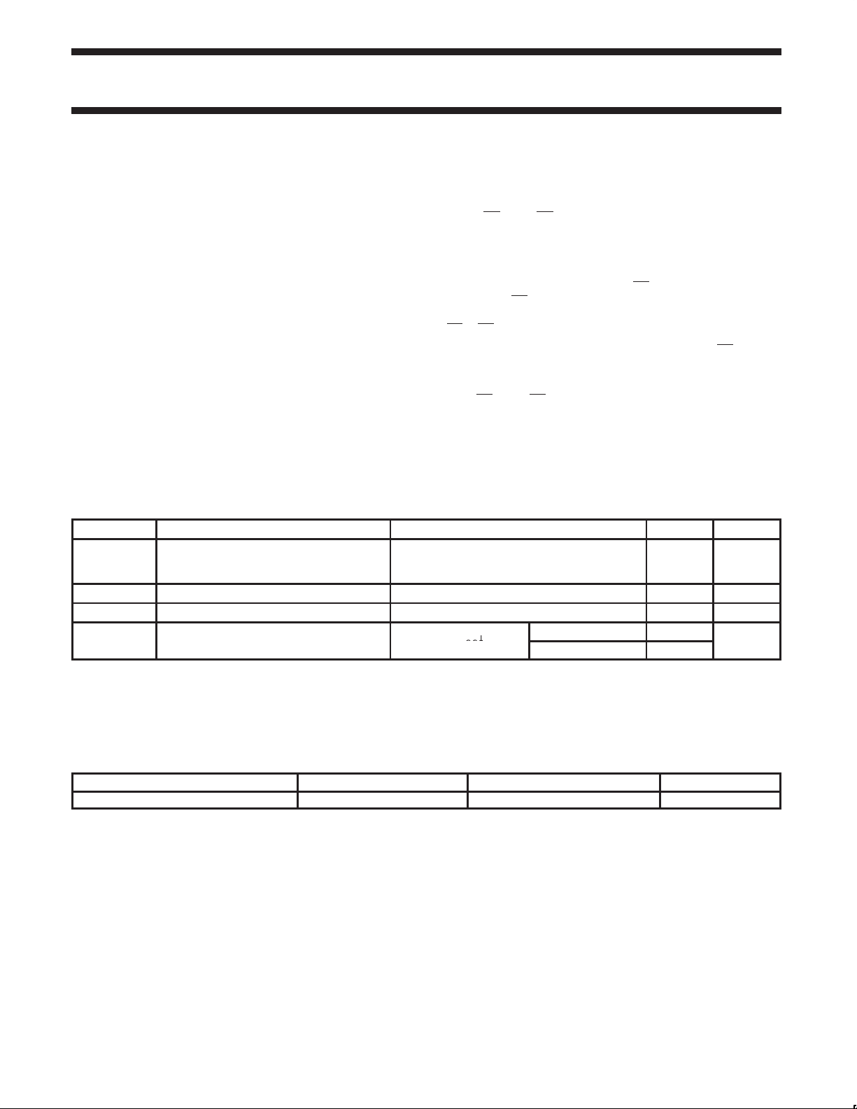
PIN CONFIGURATION
1
OE
AB
2
LE
AB
3
A0
4
GND
5
A1
6
A2
7
V
CC
8
A3
9
A4
10
A5
11
GND
12
A6
13
A7
14
A8
15
A9
16
A10
17
A11
18
GND
19
A12
20
A13
21
A14
22
V
CC
23
A15
24
A16
25
GND
26
A17
OE
27
BA
LE
28
BA
56
CE
55
CP
54
B0
53
GND
52
B1
51
B2
50
V
49
B3
48
B4
47
B5
GND
46
45
B6
B7
44
43
B8
B9
42
41
B10
B11
40
39
GND
B12
38
37
B13
36
B14
35
V
34
B15
33
B16
32
GND
31
B17
30
CP
CE
29
SW00129
CC
CC
PIN DESCRIPTION
AB
AB
BA
BA
PIN NUMBER SYMBOL NAME AND FUNCTION
1 OE
2 LE
AB
AB
Output enable A-to-B
Latch enable A-to-B
3, 5, 6, 8, 9,
10, 12, 13, 14,
15, 16, 17, 19,
A0 to A17 Data inputs/outputs
20, 21, 23, 24,
26
4, 11, 18, 25,
32, 39, 46, 53
7, 22, 35, 50 V
27 OE
28 LE
29 CE
30 CP
GND Ground (0V)
CC
BA
BA
BA
BA
Positive supply voltage
Output enable B-to-A
Latch enable B-to-A
Clock enable B-to-A
Clock input B-to-A
54, 52, 51, 49,
48, 47, 45, 44,
43, 42, 41, 40,
B0 to B17 Data inputs/outputs
38, 37, 36, 34,
33, 31
55 CP
56 CE
AB
AB
Clock input A-to-B
Clock enable A-to-B
LOGIC SYMBOL
3
5
6
8
9
10
12
13
14
15
16
17
19
20
21
23
24
26
OE
1
LE
2
CP
55
CE
56
1998 Sep 24
A0
A1
A2
A3
A4
A5
A6
A7
A8
A9
A10
A11
A12
A13
A14
A15
A16
A17
AB
AB
AB
B0
54
B1
52
B2
51
B3
49
B4
48
B5
47
B6
45
B7
44
B8
43
B9
42
B10
41
B11
40
B12
38
B13
37
B14
36
B15
34
B16
33
B17
31
OE
AB
BA
LE
BA
CP
BA
CE
BA
SW00130
27
28
30
29
3
Page 4
Philips Semiconductors Product specification
OUTPUTS
STATUS
74ALVCH1660118-bit universal bus transceiver (3-State)
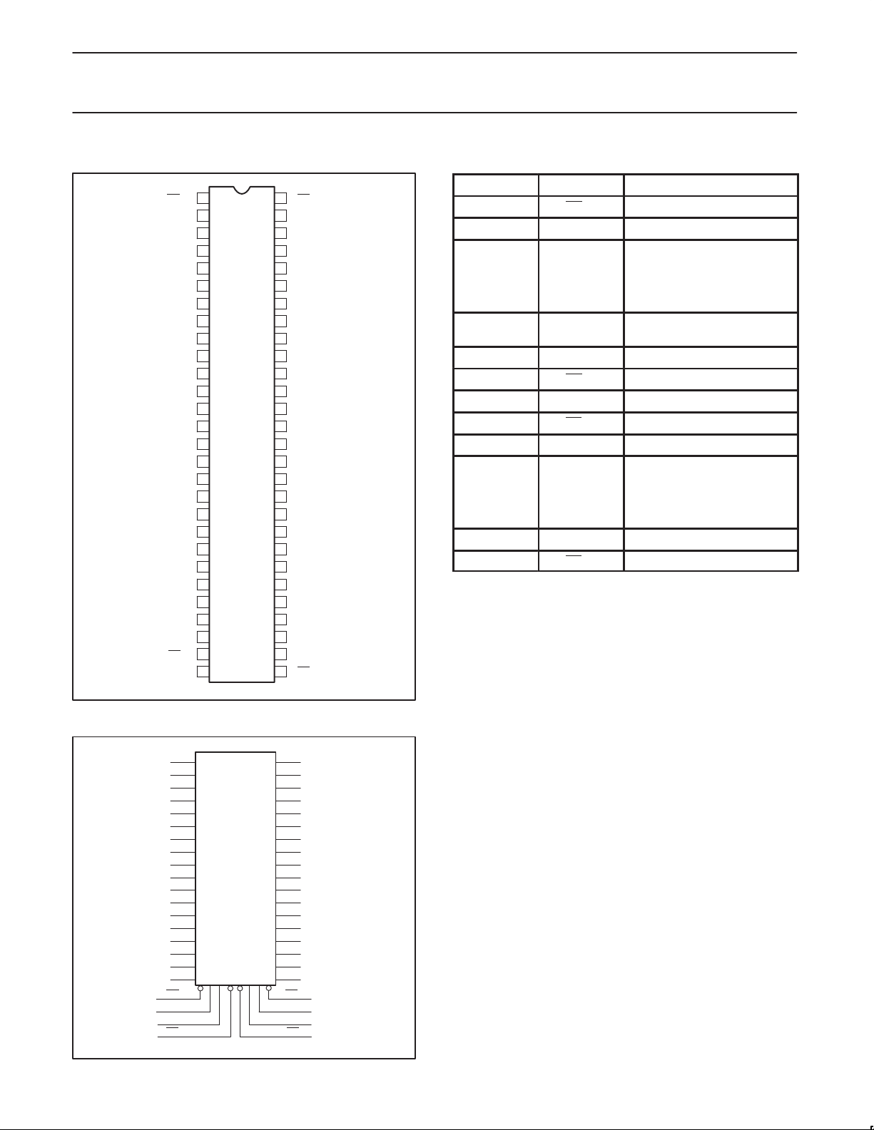
LOGIC DIAGRAM (one section)
OE
AB
CE
AB
LE
AB
CP
AB
CP
BA
LE
BA
CE
BA
OE
BA
CE
C1
A1
CE
C1
CP
1D
CP
1D
B1
18 IDENTICAL CHANNELS
SW00132
FUNCTION TABLE
INPUTS
CE
XX
X H X X X Z Disabled
X
X
H L L X X NC Hold
L
L
L
L
XX = AB for A-to-B direction, BA for B-to-A direction
H = HIGH voltage level
L = LOW voltage level
h = HIGH state must be present one setup time before the LOW-to-HIGH transition of CP
l = LOW state must be present one setup time before the LOW-to-HIGH transition of CP
X = Don’t care
↑ = LOW-to-HIGH level transition
NC = No change
Z = High impedance “off” state
OE
XX
L
L
L
L
L
L
LE
XX
H
H
L
L
L
L
CP
XX
X
X
↑
↑
L
H
DATA
H
L
h
l
X
X
H
L
H
L
NC Hold
XX
XX
Transparent
Clock + display
1998 Sep 24
4
Page 5

Philips Semiconductors Product specification
74ALVCH1660118-bit universal bus transceiver (3-State)
LOGIC SYMBOL (IEEE/IEC)
OE
CE
CP
LE
OE
CE
CP
1
AB
56
AB
55
AB
2
AB
27
BA
29
BA
30
BA
28
LE
BA
3
A0
5
A1
6
A2
8
A3
9
A4
10
A5
12
A6
13
A7
14
A8
15
A9
16
A10
17
A11
19
A12
20
A13
21
A14
23
A15
24
A16
26
A17
EN1
G2
2C3
C3
G2
EN4
G5
5C6
C6
G5
3D
46D
BUSHOLD CIRCUIT
V
CC
Data Input
54
1
B0
52
B1
51
B2
49
B3
48
B4
47
B5
45
B6
44
B7
43
B8
42
B9
41
B10
40
B11
38
B12
37
B13
36
B14
34
B15
33
B16
31
B17
SW00133
To internal circuit
SW00050
1998 Sep 24
5
Page 6

Philips Semiconductors Product specification
SYMBOL
PARAMETER
CONDITIONS
UNIT
V
V
V
DC in ut voltage
V
74ALVCH1660118-bit universal bus transceiver (3-State)
RECOMMENDED OPERATING CONDITIONS
LIMITS
MIN MAX
DC supply voltage 2.5V range (for max. speed
performance @ 30 pF output load)
CC
DC supply voltage 3.3V range (for max. speed
performance @ 50 pF output load)
T
V
V
amb
tr, t
O
DC Input voltage range 0 V
I
DC output voltage range 0 V
Operating free-air temperature range –40 +85 °C
Input rise and fall times
f
VCC = 2.3 to 3.0V
VCC = 3.0 to 3.6V
ABSOLUTE MAXIMUM RATINGS
In accordance with the Absolute Maximum Rating System (IEC 134)
Voltages are referenced to GND (ground = 0V)
SYMBOL
I
GND
V
CC
I
IK
I
I
OK
V
O
I
O
, I
T
stg
P
TOT
DC supply voltage –0.5 to +4.6 V
DC input diode current VI 0 –50 mA
DC output diode current V
DC output voltage Note 1 –0.5 to VCC +0.5 V
DC output source or sink current VO = 0 to V
DC VCC or GND current
CC
Storage temperature range –65 to +150 °C
Power dissipation per package
–plastic thin-medium-shrink (TSSOP)
NOTE:
1. The input and output voltage ratings may be exceeded if the input and output current ratings are observed.
PARAMETER CONDITIONS RATING UNIT
p
For control pins
For data inputs
VCC or VO 0
O
1
1
CC
For temperature range: –40 to +125 °C
above +55°C derate linearly with 8 mW/K 600
2.3 2.7
3.0 3.6
0
0
20
10
–0.5 to +4.6
–0.5 to VCC +0.5
50
50
100
CC
CC
V
V
ns/V
mA
mA
mA
mW
1998 Sep 24
6
Page 7

Philips Semiconductors Product specification
VIHHIGH level Input voltage
V
VILLOW level Input voltage
V
V
V
V
V
I
100µA
V
0.2
V
VOHHIGH level output voltage
V
V
V
V
V
I
100µA
GND
0.20
V
V
µ
I
g
V
V
GND
µ
I
Bus hold LOW sustaining current
A
I
Bus hold HIGH sustaining current
A
74ALVCH1660118-bit universal bus transceiver (3-State)
DC ELECTRICAL CHARACTERISTICS
Over recommended operating conditions. V oltage are referenced to GND (ground = 0 V).
LIMITS
SYMBOL PARAMETER TEST CONDITIONS Temp = -40°C to +85°C UNIT
1
MAX
CC
0.08
CC
0.26
CC
0.14
CC
0.09
CC
0.28
CC
0.1 5
0.1 10 µA
V
A
µ
µ
p
p
p
V
I
OZ
I
CC
∆I
BHL
BHH
I
BHLO
I
BHHO
LOW level output voltage
OL
I
Input leakage current
I
3-State output OFF-state current
Quiescent supply current VCC = 2.3 to 3.6V; VI = VCC or GND; IO = 0 0.2 40 µA
Additional quiescent supply current VCC = 2.3V to 3.6V; VI = VCC – 0.6V; IO = 0 150 750 µA
CC
Bus hold LOW overdrive current VCC = 3.6V
Bus hold HIGH overdrive current VCC = 3.6V
NOTES:
1. All typical values are at T
2. Valid for data inputs of bus hold parts.
amb
= 25°C.
MIN TYP
VCC = 2.3 to 2.7V 1.7 1.2
VCC = 2.7 to 3.6V 2.0 1.5
VCC = 2.3 to 2.7V 1.2 0.7
VCC = 2.7 to 3.6V 1.5 0.8
= 2.3 to 3.6V;
CC
;
=
I
VCC = 2.3V; VI = VIH or VIL; IO = –6mA V
VCC = 2.3V; VI = VIH or VIL; IO = –12mA V
VCC = 2.7V; VI = VIH or VIL; IO = –12mA V
VCC = 3.0V; VI = VIH or VIL; IO = –12mA V
VCC = 3.0V; VI = VIH or V
= 2.3 to 3.6V;
CC
;
=
I
;
or
;
IH
IO = –24mA VCC1.0 V
IL;
or
IH
= –
IL
O
;
;
=
IL
O
CC
CC
CC
CC
CC
0.3 V
0.6 V
0.5 V
0.6 V
VCC = 2.3V; VI = VIH or VIL; IO = 6mA 0.07 0.40 V
VCC = 2.3V; VI = VIH or VIL; IO = 12mA 0.15 0.70
VCC = 2.7V; VI = VIH or VIL; IO = 12mA 0.14 0.40
VCC = 3.0V; VI = VIH or V
= 2.3 to 3.6V;
CC
=
or
I
CC
;
IO = 24mA 0.27 0.55
IL;
VCC = 2.7 to 3.6V; VI = VIH or VIL;
VO = VCC or GND
VCC = 2.3V; VI = 0.7V
VCC = 3.0V; VI = 0.8V
VCC = 2.3V; VI = 1.7V
VCC = 3.0V; VI = 2.0V
2
2
2
2
2
2
45 –
75 150
–45
–75 –175
500 µA
–500 µA
1998 Sep 24
7
Page 8

Philips Semiconductors Product specification
t
2
ns
74ALVCH1660118-bit universal bus transceiver (3-State)
AC CHARACTERISTICS FOR VCC = 2.3V TO 2.7V RANGE
GND = 0V; tr = tf ≤ 2.0ns; CL = 30pF
LIMITS
SYMBOL PARAMETER WAVEFORM VCC = 2.5V ± 0.2V UNIT
1
MAX
ns
ns
ns
Propagation delay
An, Bn to Bn, An
t
PHL/tPLH
Propagation delay
LE
AB,
Propagation delay
CP
AB,
t
PZH/tPZL
t
PHZ/tPLZ
3-State output enable time
OE
BA,
3-State output enable time
OE
BA,
Pulse width HIGH
LEAB or LE
W
Pulse width HIGH or LOW
CPAB, CP
Set-up time
An, Bn to CPAB, CP
t
SU
Set-up time
An, Bn to LE
Set-up time
CE
AB,
Hold time
An, Bn to CPAB, CP
t
h
Hold time
An, Bn to LEAB, LE
Hold time
CE
AB,
f
MAX
Maximum clock frequency 150 390 – MHz
NOTE:
1. All typical values are at V
LEBA to Bn, An
CPBA to Bn, An
OEAB to An,Bn
OEAB to An,Bn
BA
BA
BA
LE
AB,
BA
CEBA to CPAB, CP
BA
BA
CEBA to CPAB, CP
= 2.5V and T
CC
BA
BA
amb
= 25°C.
MIN TYP
1.0 3.1 5.2
1, 2
1.0 3.6 6.2
1.0 3.4 5.9
3 1.1 3.1 5.3 ns
3 1.4 2.8 4.9 ns
3.3 1.6 –
3.3 2.0 –
2.3 –0.2 –
4
1.3 0.1 –
2.0 –0.4 –
1.2 0.3 –
4
1.3 0.2 –
1.1 0.4 –
1998 Sep 24
8
Page 9

Philips Semiconductors Product specification
t
2
ns
74ALVCH1660118-bit universal bus transceiver (3-State)
AC CHARACTERISTICS FOR VCC = 3.0V TO 3.6V RANGE AND VCC = 2.7V
GND = 0V; tr = tf = 2.5ns; CL = 50pF
LIMITS
SYMBOL P ARAMETER WAVEFORM VCC = 3.3V ±0.3V VCC = 2.7V UNIT
MIN TYP1MAX MIN TYP MAX
Propagation delay
An, Bn to Bn, An
t
PHL/tPLH
Propagation delay
LE
, LEBA to Bn, An
AB
Propagation delay
CPAB, CPBA to Bn, An
t
PZH/tPZL
t
PHZ/tPLZ
3-State output enable time
OEBA to An
3-State output disable time
OE
to An
BA
LE pulse width
LEAB, LEBA to CPAB, CP
W
LE pulse width HIGH or LOW
CPAB, CP
Set-up time
An, Bn to CPAB, CP
t
SU
Set-up time
An, Bn to LEAB, LE
Set-up time
CEAB, CEBA to CPAB, CP
Hold time
An, Bn to CPAB, CP
t
h
Hold time
An, Bn to LEAB, LE
Hold time
CEAB, CEBA to CPAB, CP
f
MAX
Maximum clock frequency 150 340 150 333 MHz
NOTE:
1. All typical values are at V
BA
= 3.3V and T
CC
BA
BA
BA
BA
BA
BA
BA
amb
1, 2
3 1.1 2.8 5.2 3.3 6.1 ns
3 1.2 3.2 4.4 3.3 4.8 ns
4
4
= 25°C.
1.0 2.8 4.2 3.1 4.7
1.0 3.1 4.9 3.4 5.4
1.3 3.1 5.0 3.5 5.8
3.3 0.9 3.3 0.7
3.3 0.9 3.3 1.2
2.1 –0.2 2.4 0.0
1.1 0.3 1.2 –0.2
1.7 –0.2 2.0 –0.7
1.0 –0.1 1.1 0.3
1.4 0.1 1.6 0.1
1.1 0.4 1.2 0.6
ns
ns
ns
1998 Sep 24
9
Page 10

Philips Semiconductors Product specification
ЙЙЙЙЙЙЙ
ЙЙЙЙЙЙЙ
74ALVCH1660118-bit universal bus transceiver (3-State)
AC WAVEFORMS
VCC = 2.3 TO 2.7 V RANGE
= 0.5 V
1. V
M
2. V
= VOL + 0.15V
X
= VOH – 0.15V
3. V
Y
4. V
= V
I
5. VOL and VOH are the typical output voltage drop that occur with
CC
the output load.
= 3.0 TO 3.6 V RANGE AND VCC = 2.7 V
V
CC
1. V
= 1.5 V
M
= VOL + 0.3V
2. V
X
3. V
= VOH – 0.3V
Y
= 2.7 V
4. V
I
5. V
and VOH are the typical output voltage drop that occur with
OL
the output load.
V
I
An, Bn
INPUT
GND
V
OH
Bn, An
OUTPUT
V
OL
V
M
t
PHL
V
M
t
PLH
SW00063
Waveform 1. Input (An, Bn) to output (Bn, An) propagation
delays
M
t
PHL
1/f
max
t
W
V
M
t
PLH
SW00134
LE
XX
INPUT
CP
XX
INPUT
GND
V
OH
An, Bn
OUTPUT
V
OL
V
I
V
Waveform 2. Latch enable input (LEAB,LEBA) and clock pulse
input (CP
, CPBA) to output propagation delays and their
AB
pulse width
V
I
OEXX INPUT
GND
V
M
V
I
An, Bn
INPUT
GND
V
I
, LE
CP
XX
XX
INPUT
GND
NOTE: The unshaded areas indicate when the input is permitted
to change for predictable output performance.
V
M
t
h
t
SU
V
M
t
h
t
SU
SW00128
Waveform 4. Data set-up and hold times for the An and Bn
inputs to the LE
, LEBA, CPAB and CPBA inputs
AB
TEST CIRCUIT
S
V
IN
V
CC
2.7V
1
RL=500 Ω
RL=500 Ω
OUT
2V
V
CC
PULSE
GENERATOR
V
IN
D.U.T.
R
T
V
OUT
C
L
Test Circuit for 3-State Outputs
SWITCH POSITION
TEST SWITCH
t
PLH/tPHL
t
PLZ/tPZL
t
PHZ/tPZH
Open
2V
GND
CC
V
CC
2.7V
2.7 – 3.6V
DEFINITIONS
RL =Load resistor
C
= Load capacitance includes jig and probe capacitance
L
=T ermination resistance should be equal to Z
R
T
of pulse generators.
Load circuitry for switching times
CC
Open
GND
SW00047
V
CC
OUTPUT
LOW-to-OFF
OFF-to-LOW
V
OL
V
OH
OUTPUT
HIGH-to-OFF
OFF-to-HIGH
GND
Waveform 3. 3-State enable and disable times
1998 Sep 24
t
PLZ
outputs
enabled
t
PHZ
t
PZL
V
t
PZH
M
V
M
outputs
enabled
SW00127
V
X
V
Y
outputs
disabled
10
Page 11

Philips Semiconductors Product specification
74ALVCH1660118-bit universal bus transceiver (3-State)
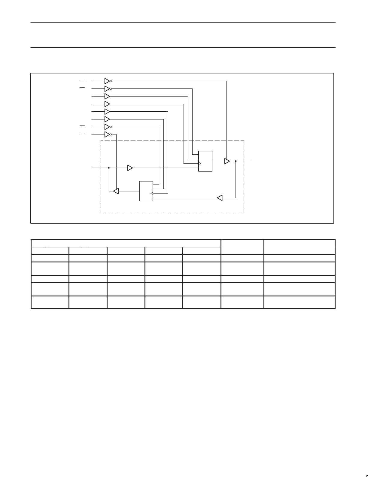
TSSOP56: plastic thin shrink small outline package; 56 leads; body width 6.1mm SOT364-1
1998 Sep 24
11
Page 12

Philips Semiconductors Product specification
74ALVCH1660118-bit universal bus transceiver (3-State)
DEFINITIONS
Data Sheet Identification Product Status Definition
Objective Specification
Preliminary Specification
Product Specification
Formative or in Design
Preproduction Product
Full Production
Philips Semiconductors and Philips Electronics North America Corporation reserve the right to make changes, without notice, in the products,
including circuits, standard cells, and/or software, described or contained herein in order to improve design and/or performance. Philips
Semiconductors assumes no responsibility or liability for the use of any of these products, conveys no license or title under any patent, copyright,
or mask work right to these products, and makes no representations or warranties that these products are free from patent, copyright, or mask
work right infringement, unless otherwise specified. Applications that are described herein for any of these products are for illustrative purposes
only. Philips Semiconductors makes no representation or warranty that such applications will be suitable for the specified use without further testing
or modification.
LIFE SUPPORT APPLICA TIONS
Philips Semiconductors and Philips Electronics North America Corporation Products are not designed for use in life support appliances, devices,
or systems where malfunction of a Philips Semiconductors and Philips Electronics North America Corporation Product can reasonably be expected
to result in a personal injury. Philips Semiconductors and Philips Electronics North America Corporation customers using or selling Philips
Semiconductors and Philips Electronics North America Corporation Products for use in such applications do so at their own risk and agree to fully
indemnify Philips Semiconductors and Philips Electronics North America Corporation for any damages resulting from such improper use or sale.
Philips Semiconductors
811 East Arques Avenue
P.O. Box 3409
Sunnyvale, California 94088–3409
Telephone 800-234-7381
This data sheet contains the design target or goal specifications for product development. Specifications
may change in any manner without notice.
This data sheet contains preliminary data, and supplementary data will be published at a later date. Philips
Semiconductors reserves the right to make changes at any time without notice in order to improve design
and supply the best possible product.
This data sheet contains Final Specifications. Philips Semiconductors reserves the right to make changes
at any time without notice, in order to improve design and supply the best possible product.
Copyright Philips Electronics North America Corporation 1998
All rights reserved. Printed in U.S.A.
Date of release: 06-98
Document order number: 9397–750–04798
1998 Sep 24
12
 Loading...