

Page 1
74ALVCH16374
LOW VOLTAGE CMOS 16-BIT D-TYPE FLIP-FLOP (3-STATE)
WITH 3.6V TOLERANT INPUTS AND OUTPUTS
■ 3.6V TOLERANT INPUTS AND OUTPUTS
■ HIGH SPEED :
t
= 4.2 ns (MAX.) at VCC=3.0to3.6V
PD
t
= 5.3 ns (MAX.) at VCC=2.3to2.7V
PD
t
= 6.5 ns (MAX.) at VCC=1.65V
PD
■ POWER DOWN PROTECTION ON INPUTS
AND OUTPUTS
■ SYMMETRICAL OUTPUT IMPEDANCE:
|=IOL= 24mA (MIN) at VCC=3.0V
|I
OH
|I
|=IOL= 18mA (MIN) at VCC=2.3V
OH
|I
|=IOL=4mA(MIN)atVCC= 1.65V
OH
■ OPERATING VOLTAGE RAN GE:
V
(OPR) = 1.65V to 3.6V
CC
■ PIN AND FUNCTION COMPATIBLE WITH
74 SERIES 16374
■ BUS HOLD PROVIDED ON DATA INPUTS
■ LATCH-UP PE RFO RMANCE E XCEEDS
300mA (JESD 17)
■ ESD PERFORMANCE:
HBM > 2000V (MIL STD 883 method 3015);
MM > 200V
ORDER CODES
PACKAGE TUBE T & R
TSSOP 74ALVCH16374TTR
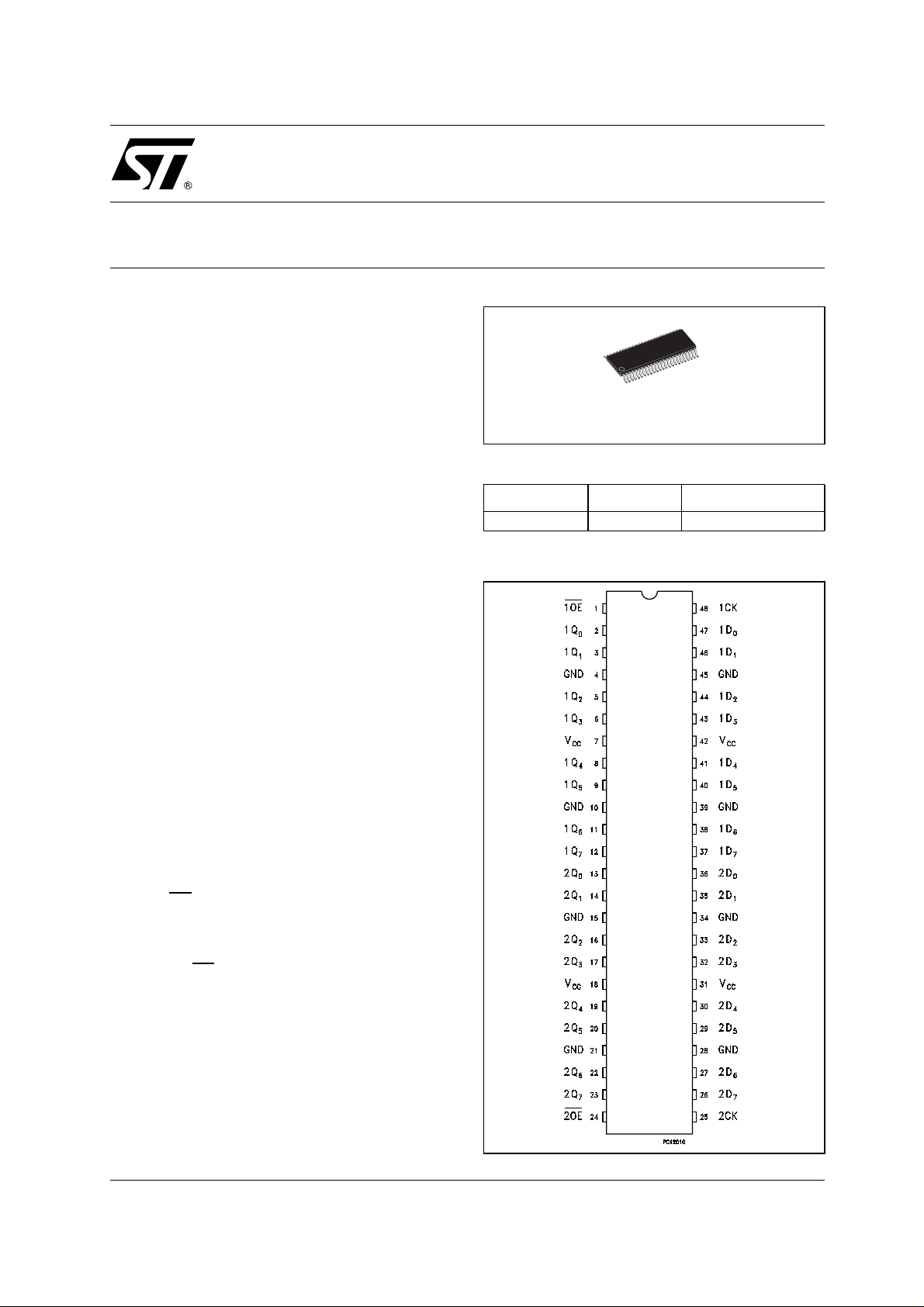
PIN CO NNE CTION
TSSOP
DESCRIPTION
The 74ALVCH16374 is a low voltage CMOS 16
BIT D-TYPEFLIP-FLOP with3 STATEOUTPUTS
NON INVERTING fabricated with sub-micron
silicon gate and five-layer metal wiring C
2
MOS
technology. It is ideal for low power and very high
speed 1.65 to 3.6V applications; it can be
interfaced to 3.6V signal environment for both
inputs and outputs.
These 16 bit D-TYPE flip-flops are controlled by
two clock inputs (nCK ) and two output enable
inputs (nOE
).
Onthepositivetransitionofthe(nCK),thenQ
outputs will be set to the logic stat e that were
setup at the nD inputs.
While the (nOE
) in put is low, the outputs (nQ) will
be in a normal state (HIGH or LOW logic level)
and while high level the outputs will be in a high
impedance sta te. Any output control does not
affect the internal operation of flip flops; that is, the
old data can be ret ained or the new data can be
entered even while the outputs are off.
All inputs and outputs are equipped with
protection circuits aga inst static discharge, giving
them 2KV ESD immunity and transient exc ess
voltage.
1/11February 2003
Page 2
74ALVCH16374
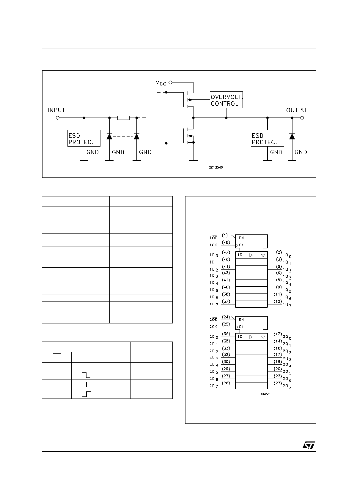
INPUT AND OUTPUT EQUIVALENT CIRCUIT
PIN DESCRIPTION
PIN No SYMBOL NAME AND FUNCTION
1 1OE
2, 3,5,6,8,9,
11, 12
13,14,16, 17,
19, 20, 22, 23
24 2OE
25 2CK Clock Input
36,35,33, 32,
30, 29, 27, 26
47,46,44, 43,
41, 40, 38, 37
48 1CK Clock Input
4, 10, 15, 21,
28, 34, 39, 45
7, 18, 31, 42 V
1Q0 to 1Q7 3-State Outputs
2Q0 to 2Q7 3-State Outputs
2D0 to 2D7 Data Inputs
1D0 to 1D7 Data Inputs
GND Ground (0V)
CC
3 State Output Enable
Input (Active LOW)
3 State Output Enable
Input (Active LOW)
Positive Supply Voltage
TRUTH TABLE
INPUTS OUTPUT
OE
HXX Z
L X NO CHANGE
LLL
LHH
X : Don‘t Care
Z : High Impedance
CK D Q
IEC LOGIC SYMBOLS
2/11
Page 3
74ALVCH16374
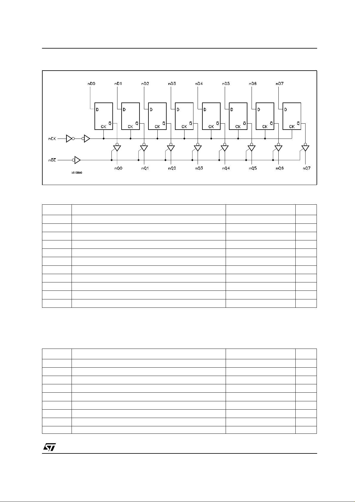
LOGIC DIAGRAM
ABSOLUTE MAXIMUM RATINGS
Symbol Parameter Value Unit
V
CC
V
V
V
I
IK
I
OK
I
or I
I
CC
P
T
stg
T
Absolute Maximum Ratings are those values beyond which damage tothe device may occur. Functional operation under these conditions is
not implied
absolute maximum rating must be observed
1) I
O
2) V
<GND,VO>V
O
Supply Voltage
DC Input Voltage
I
DC Output Voltage (OFF State)
O
DC Output Voltage (High or Low State) (note 1) -0.5 to VCC+ 0.5
O
DC Input Diode Current
DC Output Diode Current (note 2)
DC Output Current
O
DC VCCor Ground Current per Supply Pin
GND
Power Dissipation
D
Storage Temperature
Lead Temperature (10 sec)
L
CC
-0.5 to +4.6 V
-0.5 to +4.6 V
-0.5 to +4.6 V
V
-50 mA
-50 mA
± 50 mA
± 100 mA
400 mW
-65 to +150 °C
300 °C
RECOMMENDED OPERATING CONDITIONS
Symbol Parameter Value Unit
V
CC
V
V
V
I
OH,IOL
I
OH,IOL
I
OH,IOL
T
dt/dv Input Rise and Fall Time (note 1) 0 to 10 ns/V
1) VINfrom0.8V to 2Vat VCC=3.0V
Supply Voltage
Input Voltage
I
Output Voltage (OFF State)
O
Output Voltage (High or Low State) 0 to V
O
High or Low Level Output Current (VCC= 3.0 to 3.6V)
High or Low Level Output Current (VCC= 2.3 to 2.7V)
High or Low Level Output Current (VCC= 1.65V)
Operating Temperature
op
1.65 to 3.6 V
-0.3 to 3.6 V
0 to 3.6 V
CC
± 24 mA
± 12 mA
± 4mA
-55 to 125 °C
V
3/11
Page 4
74ALVCH16374
DC SPECIFICATIONS
Test Condition Value
Symbol Parameter
V
V
V
I
IHOLD
High Level Input
IH
Voltage
V
Low Level Input
IL
Voltage
High Level Output
OH
Voltage
Low Level Output
OL
Voltage
Input Leakage
I
I
Current
Bus Hold Input
Leakage Current
Power Off Leakage
I
off
Current
High Impedance
I
OZ
Output Leakage
Current
I
∆I
Quiescent Supply
CC
Current
CCICC
incr. per Input 3.0 to 3.6 VIH=VCC- 0.6V 500 750 µA
V
CC
(V)
-40 to 85 °C -55 to 125 °C
Min. Max. Min. Max.
1.65 to 1.95 0.65 Vcc 0.65 Vcc
2.3 to 2.7 1.7 1.7
2.7 to 3.6 2.0 2.0
1.65 to 1.95 0.35 Vcc 0.35 Vcc
2.3 to 2.7 0.7 0.7
2.7 to 3.6 0.8 0.8
=-100 µAVCC-0.2 VCC-0.2
1.65 to 3.6
1.65
2.3
2.3
2.7
3.0
3.0
1.65 to 3.6
1.65
2.3
2.3
2.7
3.0
3.6
1.65
1.65
2.3
2.3
3.0
3.0
3.6
0V
3.6 VI=VIHor V
3.6 VI=VCCor GND
I
O
=-4 mA
I
O
=-6 mA
I
O
I
=-12 mA
O
=-12 mA
I
O
=-12 mA
I
O
=-24 mA
I
O
IO=100 µA
=4 mA
I
O
=6 mA
I
O
=12 mA
I
O
=12 mA
I
O
=24 mA
I
O
= 0 or 3.6V
V
I
VI=0.58 V
=1.07 V
V
I
=0.7 V
V
I
=1.7 V
V
I
=0.8 V
V
I
=2 V
V
I
V
= 0 to 3.6V
I
or VO=3.6V 10 20 µA
I
VO= 0 to V
IL
CC
1.2 1.2
2.0 2.0
1.7 1.7
2.2 2.2
2.4 2.4
2.0 2.0
0.2 0.2 V
0.45 0.45
0.4 0.4
0.7 0.7
0.4 0.4
0.55 0.55
± 5 ± 5 µA
+25 +25
-25 -25
+45 +45
-45 -45
+75 +75
-75 -75
± 500 ± 500
± 5 ± 10 µA
20 40 µA
=0
I
O
Unit
V
V
µA
4/11
Page 5

AC ELECTRICAL C HARACTERISTICS
Test Condition Value
74ALVCH16374
Symbol Parameter
t
PLHtPHL
t
PZLtPZH
t
PLZtPHZ
f
MAX
Propagation Delay
Time CK to Qn
Output Enable Time 1.65 to 1.95 30 1000 2.0 1 7.5 1 7.5
Output Disable Time 1.65 to 1.95 30 1000 2.0 1 6.5 1 6.5
t
Setup TIme, HIGH or
s
LOW level Dn to CK
t
Hold Time High or
h
LOW level Dn to CK
t
CK Pulse Width,
w
HIGH
Maximum Clock
Pulse Frequency
V
CC
(V)
C
(pF)
R
L
(Ω)
= t
t
L
s
(ns)
-40 to 85 °C -55 to 125 °C
r
Min. Max. Min. Max.
1.65 to 1.95 30 1000 2.0 1 6.5 1 6.5
2.3 to 2.7 30 500 2.0 1 5.3 1 5.3
2.7 50 500 2.5 1 4.9 1 4.9
3.0 to 3.6 50 500 2.5 1 4.2 1 4.2
2.3 to 2.7 30 500 2.0 1 6.2 1 6.2
2.7 50 500 2.5 1 5.9 1 5.9
3.0 to 3.6 50 500 2.5 1 4.8 1 4.8
2.3 to 2.7 30 500 2.0 1 5.3 1 5.3
2.7 50 500 2.5 1 4.7 1 4.7
3.0 to 3.6 50 500 2.5 1 4.3 1 4.3
1.65 to 1.95 30 1000 2.0 1 1
2.3 to 2.7 30 500 2.0 1 1
2.7 50 500 2.5 1 1
3.0 to 3.6 50 500 2.5 1 1
1.65 to 1.95 30 1000 2.0 1.5 1.5
2.3 to 2.7 30 500 2.0 1.5 1.5
2.7 50 500 2.5 1.5 1.5
3.0 to 3.6 50 500 2.5 1.5 1.5
1.65 to 1.95 30 1000 2.0 4 4
2.3 to 2.7 30 500 2.0 3.3 3.3
2.7 50 500 2.5 3.3 3.3
3.0 to 3.6 50 500 2.5 3.3 3.3
1.65 to 1.95 30 1000 2.0 120 120
2.3 to 2.7 30 500 2.0 150 150
2.7 50 500 2.5 200 200
3.0 to 3.6 50 500 2.5 300 300
Unit
ns
ns
ns
ns
ns
ns
MHz
5/11
Page 6

74ALVCH16374
CAPACITIVE CHARACTERISTICS
Test Condition Value
=25°C
Symbol Parameter
V
CC
(V)
C
C
C
OUT
C
C
1) CPDis defined as the value of the IC’s internal equivalent capacitance which is calculated from the operating current consumption without
load. (Refer to Test Circuit). Average operating current can be obtained by the following equation. I
circuit)
Input Capacitance Control
IN
Inputs
Input Capacitance Data Inputs
IN
Output Capacitance
Power Dissipation Capacitance
PD
Output enabled (note 1)
Power Dissipation Capacitance
PD
Output disabled (note 1)
3.3
3.3
3.3
V
IN=VCC
VIN=VCCor GND
VIN= 0 to V
or GND
CC
3.3 fIN= 10MHz
C
V
IN
=50pF
L
= 0 or V
CC
2.5 16
3.3 5
2.5 4
TEST CIRCUIT
T
A
Min. Typ. Max.
3pF
6pF
7pF
19
CC(opr)=CPDxVCCxfIN+ICC
Unit
pF
/16 (per
TEST SWITCH
t
PLH,tPHL
t
PZL,tPLZ(VCC
t
PZL,tPLZ(VCC
t
PZH,tPHZ
RT=Z
OUT
= 3.0 to 3.6V)
= 2.3 to 2.7V) 2V
of pulse generator (typically 50Ω)
TEST CIRCUIT AND WAVE FORM SYMBOL VALUE
6/11
Symbol
V
IH
V
M
V
X
V
Y
C
L
R
L=R1
t
r=tr
3.0 to 3.6V 2.7V 2.3 to 2.7V 1.65 to 1.95V
2.7V 2.7V V
1.5V 1.5V VCC/2 VCC/2
VOL+0.3V VOL+0.3V VOL+0.15V VOL+0.15V
VOH-0.3V VOH-0.3V VOH-0.15V VOH-0.15V
50pF 50pF 30pF 30pF
500Ω 500Ω 500Ω 1000Ω
<2.5ns <2.5ns <2.0ns <2.0ns
Open
6V
CC
GND
V
CC
CC
V
CC
Page 7

74ALVCH16374
WAVEFORM 1 : PROPAGATION DEL AYS, CK MINIMUM PULSE WIDTH, Dn TO CK SETUP AND
HOLD TIMES, CK M AXIMUM FREQUENCY (f=1MHz; 50% duty cycle)
WAVEFORM 2: OUTPUT ENABLE AND DISABLE TIME (f=1MHz; 50% duty cycle)
7/11
Page 8

74ALVCH16374
WAVEFORM 3 : CK MINIMUM PULSE WIDTH (f=1MHz; 50% duty cycle)
8/11
Page 9

74ALVCH16374
TSSOP48 MECHANICAL DATA
mm. inch
DIM.
MIN. TYP MAX. MIN. TYP. MAX.
A 1.2 0.047
A1 0.05 0.15 0.002 0.006
A2 0.9 0.035
b 0.17 0.27 0.0067 0.011
c 0.09 0.20 0.0035 0.0079
D 12.4 12.6 0.488 0.496
E 8.1 BSC 0.318 BSC
E1 6. 0 6.2 0.236 0.244
e 0 .5 BSC 0.0197 BSC
K0˚ 8˚0˚ 8˚
L 0.50 0.75 0.020 0.030
A2
A
A1
b
e
D
K
c
E1
L
E
PIN 1 IDENTIFICATION
1
7065588C
9/11
Page 10

74ALVCH16374
Tape & Reel TSSOP48 MECHANICAL DATA
mm. inch
DIM.
MIN. TYP MAX. MIN. TYP. MAX.
A 330 12.992
C 12.8 13.2 0.504 0.519
D 20.2 0.795
N 60 2.362
T 30.4 1.197
Ao 8.7 8.9 0.343 0.350
Bo 13.1 13.3 0.516 0.524
Ko 1.5 1.7 0.059 0.067
Po 3.9 4.1 0.153 0.161
P 11.9 12.1 0.468 0.476
10/11
Page 11

74ALVCH16374
Information furnished is believed to be accurate and reliable. However, STMicroelectronics assumes no responsibilit y for the
consequences of use of such informatio n nor for any infringement of paten ts or o ther rig hts of t hird part ies which ma y result from
its use. No license is granted by implication or otherwise under any patent or patent rights of STMicroelectronics. Specifications
mentioned in this publication are subject to change without notice. This publication supersedes and replaces all information
previousl y suppl ied. STM icroel ectronics produc ts are not auth orized for use as c ritica l compone nts in l ife s upport dev ices or
systems without express written approval of STMicroelectronics.
Australia - Brazil - Canada - China - Finland - France - Germany - Hong Kong - India - Israel - Italy - Japan - Malaysia - Malta - Morocco
© The ST logo is a registered trademark of STMicroelectronics
© 2002 STMicroelectronics - Printed in Italy - All Rights Reserved
STMicroelectronics GROUP OF COMPANIES
Singapore - Spain - Sweden - Switzerland - United Kingdom - United States.
© http://www.st.com
11/11
 Loading...