

Page 1

74ALVCH162827
20-bit buffer/line driver, non-inverting,
with 30 termination resistors (3-State)
Product specification
IC24 Data Handbook
1998 Sep 29
INTEGRATED CIRCUITS
Page 2
Philips Semiconductors Product specification
74ALVCH162827
20-bit buffer/line driver, non-inverting, with 30Ω
termination resistors (3-State)
2
1998 Sep 29 853-2127 20100
FEA TURES
•Complies with JEDEC standard no. 8-1A.
•CMOS low power consumption
•Direct interface with TTL levels
•Current drive ± 12 mA at 3.0 V
•MULTIBYTE
TM
flow-through standard pin-out architecture
•Low inductance multiple V
CC
and GND pins for minimum noise
and ground bounce
•Integrated 30 W termination resistors
DESCRIPTION
The 74ALVCH162827 high-performance CMOS device combines
low static and dynamic power dissipation with high speed and high
output drive.
The 74ALVCH162827 20-bit buffers provide high performance bus
interface buffering for wide data/address paths or buses carrying
parity. They have NAND Output Enables (nOE
1, nOE2) for
maximum control flexibility.
The 74ALVCH162827 is designed with 30Ω series resistance in both
the pull-up and pull-down output structures. This design reduces line
noise in applications such as memory address drivers, clock drivers
and bus receivers/transmitters.
To ensure the high impedance state during power up or power
down, OE
should be tied to VCC through a pullup resistor; the
minimum value of the resistor is determined by the
current-sinking/current-sourcing capability of the driver.
Active bus-hold circuitry is provided to hold unused or floating data
inputs at a valid logic level.
QUICK REFERENCE DA TA
GND = 0V; T
amb
= 25°C; tr = tf = 2.5ns
SYMBOL
PARAMETER CONDITIONS TYPICAL UNIT
t
PHL/tPLH
Propagation delay
nAn to nYn
VCC = 2.5V , CL = 30pF
VCC = 3.3V , CL = 50pF
2.9
2.9
ns
C
I
Input capacitance 5 pF
p
p
p
1
Output enabled 14
p
CPDPower dissi ation ca acitance er latch
V
I
=
GND to V
CC
1
Output disabled 3
F
NOTES:
1. C
PD
is used to determine the dynamic power dissipation (PD in mW):
P
D
= CPD × V
CC
2
× fi + S (CL × V
CC
2
× fo) where:
f
i
= input frequency in MHz; CL = output load capacity in pF;
f
o
= output frequency in MHz; VCC = supply voltage in V;
S (C
L
× V
CC
2
× fo) = sum of outputs.
ORDERING INFORMATION
PACKAGES TEMPERATURE RANGE OUTSIDE NORTH AMERICA NORTH AMERICA DWG NUMBER
56-Pin Plastic TSSOP Type II –40°C to +85°C 74ALVCH162827DGG ACH162827DGG SOT364-1
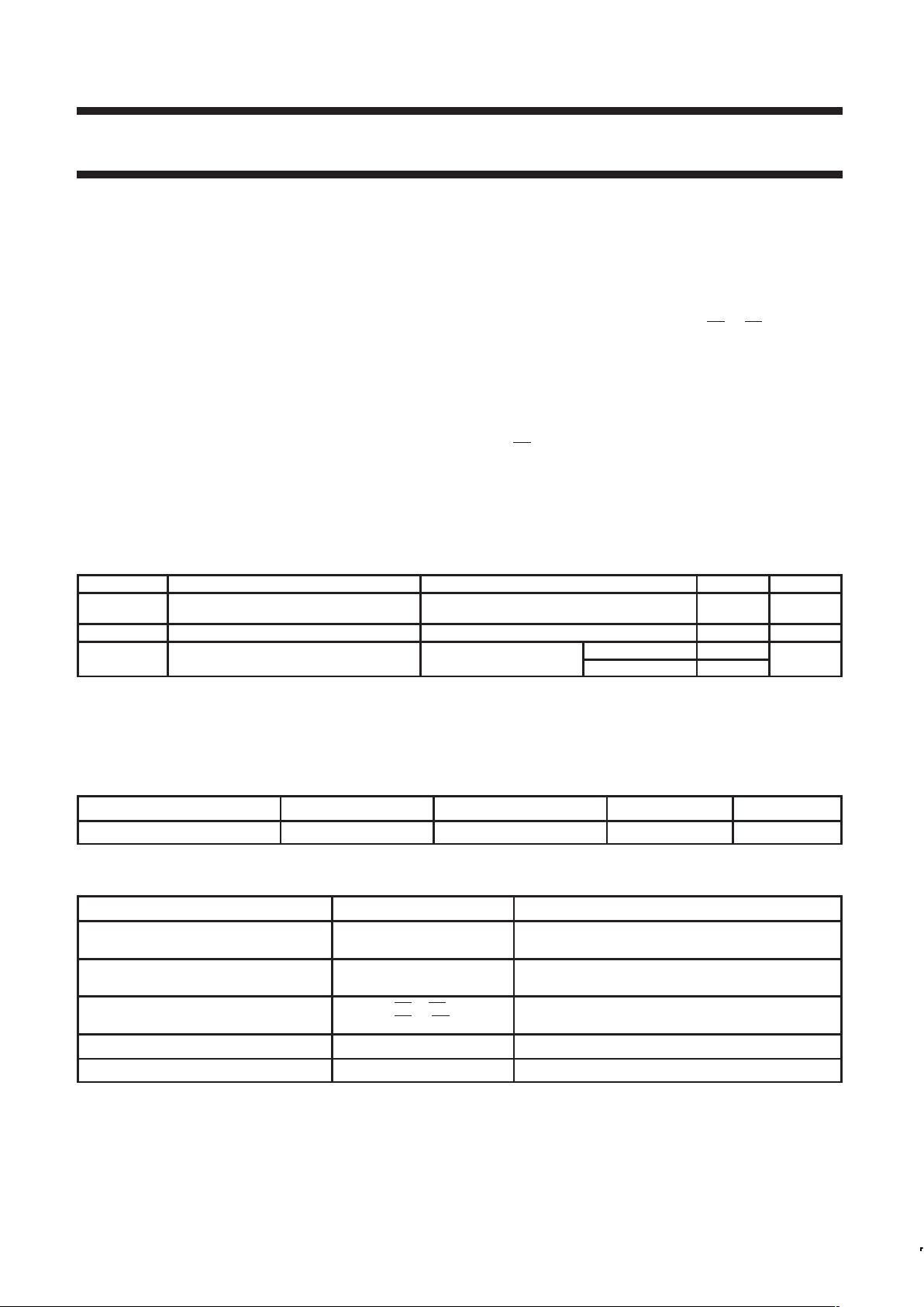
PIN DESCRIPTION
PIN NUMBER SYMBOL FUNCTION
55, 54, 52, 51, 49, 48, 47, 45, 44, 43,
42, 41, 40, 38, 37, 36, 34, 33, 31, 30
1A0 - 1A9
2A0 - 2A9
Data inputs
2, 3, 5, 6, 8, 9, 10, 12, 13, 14,
15, 16, 17, 19, 20, 21, 23, 24, 26, 27
1Y0 - 1Y9
2Y0 - 2Y9
Data outputs
1, 56,
28, 29
1OE1 1OE2,
2OE1, 2OE2
Output enable inputs (active-LOW)
4, 11, 18, 25, 32, 39, 46, 53 GND Ground (0V)
7, 22, 35, 50 V
CC
Positive supply voltage
Page 3
Philips Semiconductors Product specification
74ALVCH162827
20-bit buffer/line driver, non-inverting, with 30Ω
termination resistors (3-State)
1998 Sep 29
3
PIN CONFIGURATION
1
2
3
4
5
6
7
8
9
10
11
12
13
14
15
16
17
18
19
20
21
22
23
24
25
26
27
28 29
30
31
32
33
34
35
36
37
38
39
40
41
42
43
44
45
46
47
48
49
50
51
52
53
54
55
561OE1
1Y0
1Y1
1Y2
1Y3
1Y4
1Y5
1Y6
GND
V
CC
GND
1Y7
1Y8
1Y9
2Y0
2Y1
2Y2
GND
2Y3
2Y4
2Y5
V
CC
2Y6
2Y7
GND
2Y8
2Y9
2OE
1
1OE
2
1A0
1A1
GND
1A2
1A3
V
CC
1A4
1A5
1A6
GND
1A7
1A8
1A9
2A0
2A1
2A2
GND
2A3
2A4
2A5
V
CC
2A6
2A7
GND
2A8
2A9
2OE
2
SH00010
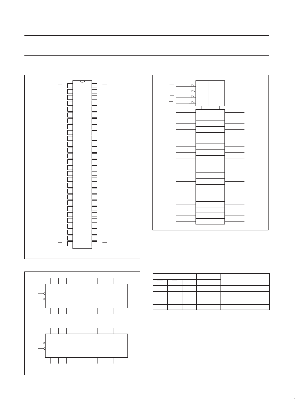
LOGIC SYMBOL
1A0 1A1 1A2 1A3 1A4 1A5 1A6 1A7
1Y0 1Y1 1Y2 1Y3 1Y4 1Y5 1Y6 1Y7
1A8 1A9
1Y8 1Y9
2A0 2A1 2A2 2A3 2A4 2A5 2A6 2A7
2Y0 2Y1 2Y2 2Y3 2Y4 2Y5 2Y6 2Y7
2A8 2A9
2Y8 2Y9
55 54 52 51 49 48 47 45 44 43
56
1
29
28
2 3 5 6 8 9 10 12 13 14
42 41 40 38 37 36 34 33 31 30
15 16 17 19 20 21 23 24 26 27
SH00011
1OE1
1OE2
2OE1
2OE2
LOGIC SYMBOL (IEEE/IEC)
EN1
1 ∇
EN2
1
2 ∇
1
SH00012
1
56
28
29
55
54
52
51
49
48
47
45
44
43
42
41
40
38
37
36
34
33
31
30
2
3
5
6
8
9
10
12
13
14
15
16
17
19
20
21
23
24
26
27
&
&
1OE1
1Y0
1Y1
1Y2
1Y3
1Y4
1Y5
1Y6
1Y7
1Y8
1Y9
2Y0
2Y1
2Y2
2Y3
2Y4
2Y5
2Y6
2Y7
2Y8
2Y9
2OE
1
1OE
2
1A0
1A1
1A2
1A3
1A4
1A5
1A6
1A7
1A8
1A9
2A0
2A1
2A2
2A3
2A4
2A5
2A6
2A7
2A8
2A9
2OE
2
FUNCTION TABLE
INPUTS OUTPUT
nOE1 nOE2 nAn nYn
OPERATING MODE
L L L L Transparent
L L H H Transparent
H X X Z High impedance
X H X Z High impedance
X = Don’t care
Z = High impedance “off” state
H = High voltage level
L = Low voltage level
Page 4

Philips Semiconductors Product specification
74ALVCH162827
20-bit buffer/line driver, non-inverting, with 30Ω
termination resistors (3-State)
1998 Sep 29
4
LOGIC DIAGRAM
nA0
nY0
nOE
1
nA1
nY1
nA2
nY2
nA3
nY3
nA4
nY4
nA5
nY5
nA6
nY6
nA7
nY7
nA8
nY8
nA9
nY9
nOE2
SH00013
RECOMMENDED OPERA TING CONDITIONS
SYMBOL PARAMETER CONDITIONS MIN MAX UNIT
DC supply voltage 2.5V range (for max. speed
performance @ 30 pF output load)
2.3 2.7
V
CC
DC supply voltage 3.3V range (for max. speed
performance @ 50 pF output load)
3.0 3.6
V
V
I
DC Input voltage range 0 V
CC
V
V
O
DC output voltage range 0 V
CC
V
T
amb
Operating free-air temperature range –40 +85 °C
tr, t
f
Input rise and fall times
VCC = 2.3 to 3.0V
VCC = 3.0 to 3.6V
0
0
20
10
ns/V
ABSOLUTE MAXIMUM RATINGS
In accordance with the Absolute Maximum Rating System (IEC 134)
Voltages are referenced to GND (ground = 0V)
SYMBOL
PARAMETER CONDITIONS RATING UNIT
V
CC
DC supply voltage –0.5 to +4.6 V
I
IK
DC input diode current
VI 0
–50 mA
V
I
DC input voltage Note 1 –0.5 to +4.6 V
I
OK
DC output diode current
V
O
VCC or VO 0
50
mA
V
O
DC output voltage Note 1 –0.5 to VCC +0.5 V
I
O
DC output source or sink current VO = 0 to V
CC 50
mA
I
GND
, I
CC
DC VCC or GND current
100
mA
T
stg
Storage temperature range –65 to +150 °C
P
TOT
Power dissipation per package
–plastic thin-medium-shrink (TSSOP)
For temperature range: –40 to +125 °C
above +55°C derate linearly with 8 mW/K 600
mW
NOTE:
1. The input and output voltage ratings may be exceeded if the input and output current ratings are observed.
Page 5

Philips Semiconductors Product specification
74ALVCH162827
20-bit buffer/line driver, non-inverting, with 30Ω
termination resistors (3-State)
1998 Sep 29
5
DC ELECTRICAL CHARACTERISTICS
Over recommended operating conditions. V oltage are referenced to GND (ground = 0 V).
LIMITS
SYMBOL PARAMETER TEST CONDITIONS Temp = -40°C to +85°C UNIT
MIN TYP
1
MAX
p
VCC = 2.3 to 2.7V 1.7 1.2
VIHHIGH level Input voltage
VCC = 2.7 to 3.6V 2.0 1.5
V
p
VCC = 2.3 to 2.7V 1.2 0.7
VILLOW level Input voltage
VCC = 2.7 to 3.6V 1.5 0.8
V
;
;
V
CC
= 2.3 to 3.6V;
V
I
=
V
IH
or
V
IL
;
I
O
= –
100µA
V
CC
0.2
V
CC
VCC = 2.3V; VI = VIH or VIL; IO = –4mA V
CC
0.4 V
CC
0.11
VCC = 2.3V; VI = VIH or VIL; IO = –6mA V
CC
0.6 V
CC
0.17
V
OH
HIGH level output voltage
VCC = 2.7V; VI = VIH or VIL; IO = –4mA V
CC
0.5 V
CC
0.09
V
VCC = 2.7V; VI = VIH or VIL; IO = –8mA V
CC
0.7 V
CC
0.19
VCC = 3.0V; VI = VIH or VIL; IO = –6mA V
CC
0.6 V
CC
0.13
VCC = 3.0V; VI = VIH or V
IL;
IO = –12mA VCC1.0 V
CC
0.27
;
;
V
CC
= 2.3 to 3.6V;
V
I
=
V
IH
or
V
IL
;
I
O
=
100µA
GND
0.20
VCC = 2.3V; VI = VIH or VIL; IO = 4mA 0.07 0.40
VCC = 2.3V; VI = VIH or VIL; IO = 6mA 0.11 0.55
V
OL
LOW level output voltage
VCC = 2.7V; VI = VIH or VIL; IO = 4mA 0.06 0.40
V
VCC = 2.7V; VI = VIH or VIL; IO = 8mA 0.13 0.60
VCC = 3.0V; VI = VIH or V
IL;
IO = 6mA 0.09 0.55
VCC = 3.0V; VI = VIH or V
IL;
IO = 12mA 0.19 0.80
;
I
I
Input leakage current
V
CC
= 2.3 to 3.6V;
0.1 5
µ
A
I
g
V
I
=
V
CC
or
GND
µ
I
OZ
3-State output OFF-state current
VCC = 2.3 to 3.6V; VI = VIH or VIL;
V
O
= VCC or GND
0.1 10 µA
I
CC
Quiescent supply current VCC = 2.3 to 3.6V; VI = VCC or GND; IO = 0 0.2 40 µA
∆I
CC
Additional quiescent supply current VCC = 2.3V to 3.6V; VI = VCC – 0.6V; IO = 0 150 750 µA
I
BHL
Bus hold LOW sustaining current VCC = 2.3V; VI = 0.7V
2
45 – µA
VCC = 2.3V; VI = 1.7V
2
–45
I
BHH
Bus hold HIGH sustaining current
VCC = 3.0V; VI = 2.0V
2
–75 –175
µ
A
I
BHLO
Bus hold LOW overdrive current VCC = 3.6V
2
500 µA
I
BHHO
Bus hold HIGH overdrive current VCC = 3.6V
2
–500 µA
NOTES:
1. All typical values are at T
amb
= 25°C.
2. Valid for data inputs of bus hold parts.
Page 6

Philips Semiconductors Product specification
74ALVCH162827
20-bit buffer/line driver, non-inverting, with 30Ω
termination resistors (3-State)
1998 Sep 29
6
AC CHARACTERISTICS FOR VCC = 2.5V ± 0.2V
GND = 0V; tr = tf ≤ 2.0ns; CL = 30pF
LIMITS
SYMBOL PARAMETER WAVEFORM VCC = 2.5 ± 0.2V UNIT
MIN TYP
1
MAX
t
PHL/tPLH
Propagation delay
nAn to nYn
1, 3 1.0 2.9 4.6 ns
t
PZH/tPZL
3-State output enable time
nOEn to nYn
2, 3 1.4 3.9 6.4 ns
t
PHZ/tPLZ
3-State output disable time
nOEn to nYn
2,3 1.7 2.2 5.9 ns
NOTE:
1. All typical values are at V
CC
= 2.5V and T
amb
= 25°C.
AC CHARACTERISTICS FOR VCC = 3.0V ± 0.3V
GND = 0V; tr = tf ≤ 2.5ns; CL = 50pF
LIMITS LIMITS
SYMBOL PARAMETER WAVEFORM VCC = 3.3 ± 0.3V VCC = 2.7V UNIT
MIN TYP
1, 2
MAX TYP
1
MAX
t
PHL/tPLH
Propagation delay
nAn to nYn
1, 3 1.5 2.9 4.2 3.1 4.7 ns
t
PZH/tPZL
3-State output enable time
nOEn to nYn
2, 3 1.6 3.7 5.4 4.4 6.5 ns
t
PHZ/tPLZ
3-State output disable time
nOEn to nYn
2, 3 1.8 3.0 4.7 3.2 5.2 ns
NOTES:
1. All typical values are at V
CC Tamb
= 25°C.
2. Typical value is measured at V
CC
= 3.3V .
Page 7

Philips Semiconductors Product specification
74ALVCH162827
20-bit buffer/line driver, non-inverting, with 30Ω
termination resistors (3-State)
1998 Sep 29
7
AC WAVEFORMS FOR VCC = 2.3V TO 2.7V
VM = 0.5 V
CC
VX = VOL + 0.15V
VY = VOH –0.15V
VOL and VOH are the typical output voltage drop that occur with the
output load.
V
I
= V
CC
AC WAVEFORMS FOR VCC = 3.0V TO 3.6V AND
VCC = 2.7V RANGE
VM = 1.5 V
V
X
= VOL + 0.3V
VY = VOH –0.3V
VOL and VOH are the typical output voltage drop that occur with the
output load.
V
I
= 2.7V
A
n
INPUT
t
PHL
t
PLH
V
OL
V
I
GND
V
OH
Y
n
OUTPUT
SH00132
V
M
V
M
Waveform 1. Input (nAx) to Output (nYx) Propagation Delays
t
PLZ
t
PZL
V
I
nOE INPUT
GND
V
CC
OUTPUT
LOW-to-OFF
OFF-to-LOW
V
OL
V
OH
OUTPUT
HIGH-to-OFF
OFF-to-HIGH
GND
outputs
enabled
outputs
enabled
outputs
disabled
t
PHZ
V
M
V
M
V
M
t
PZH
V
X
V
Y
SH00137
Waveform 2. 3-State Output Enable and Disable Times
TEST CIRCUIT AND WAVEFORM
SWITCH POSITION
PULSE
GENERATOR
R
T
V
I
D.U.T.
V
O
C
L
V
CC
RL = 500 Ω
Test Circuit for switching times
Open
GND
S
1
DEFINITIONS
V
CC
V
I
< 2.7V V
CC
TEST S
1
t
PLH/tPHL
Open
R
L
= Load resistor
C
L
= Load capacitance includes jig and probe capacitance
R
T
= Termination resistance should be equal to Z
OUT
of pulse generators.
2 V
CC
t
PLZ/tPZL
2.7V2.7–3.6V
t
PHZ/tPZH
GND
RL = 500 Ω
2 * V
CC
SV00906
Waveform 3. Load circuitry for switching times
Page 8

Philips Semiconductors Product specification
74AL VCH162827
20-bit buffer/line driver, non-inverting, with 30
termination resistors (3-State)
1998 Sep 29
8
TSSOP56: plastic thin shrink small outline package; 56 leads; body width 6.1mm SOT364-1
Page 9

Philips Semiconductors Product specification
74AL VCH162827
20-bit buffer/line driver, non-inverting, with 30
termination resistors (3-State)
1998 Sep 29
9
NOTES
Page 10

Philips Semiconductors Product specification
74AL VCH162827
20-bit buffer/line driver, non-inverting, with 30
termination resistors (3-State)
1998 Sep 29
10
Philips Semiconductors and Philips Electronics North America Corporation reserve the right to make changes, without notice, in the products,
including circuits, standard cells, and/or software, described or contained herein in order to improve design and/or performance. Philips
Semiconductors assumes no responsibility or liability for the use of any of these products, conveys no license or title under any patent, copyright,
or mask work right to these products, and makes no representations or warranties that these products are free from patent, copyright, or mask
work right infringement, unless otherwise specified. Applications that are described herein for any of these products are for illustrative purposes
only. Philips Semiconductors makes no representation or warranty that such applications will be suitable for the specified use without further testing
or modification.
LIFE SUPPORT APPLICA TIONS
Philips Semiconductors and Philips Electronics North America Corporation Products are not designed for use in life support appliances, devices,
or systems where malfunction of a Philips Semiconductors and Philips Electronics North America Corporation Product can reasonably be expected
to result in a personal injury. Philips Semiconductors and Philips Electronics North America Corporation customers using or selling Philips
Semiconductors and Philips Electronics North America Corporation Products for use in such applications do so at their own risk and agree to fully
indemnify Philips Semiconductors and Philips Electronics North America Corporation for any damages resulting from such improper use or sale.
This data sheet contains preliminary data, and supplementary data will be published at a later date. Philips
Semiconductors reserves the right to make changes at any time without notice in order to improve design
and supply the best possible product.
Philips Semiconductors
811 East Arques Avenue
P.O. Box 3409
Sunnyvale, California 94088–3409
Telephone 800-234-7381
DEFINITIONS
Data Sheet Identification Product Status Definition
Objective Specification
Preliminary Specification
Product Specification
Formative or in Design
Preproduction Product
Full Production
This data sheet contains the design target or goal specifications for product development. Specifications
may change in any manner without notice.
This data sheet contains Final Specifications. Philips Semiconductors reserves the right to make changes
at any time without notice, in order to improve design and supply the best possible product.
Copyright Philips Electronics North America Corporation 1998
All rights reserved. Printed in U.S.A.
Date of release: 06-98
Document order number: 9397-750-04603
 Loading...