

Page 1
1/10July 2003
■ 3.6V TOLERANT INPUTS A N D OUTPUTS
■ HIGH SPEED:
t
PD
= 3.0 ns (MAX.) at VCC=3.0to3.6V
t
PD
= 3.7 ns (MAX.) at VCC=2.3to2.7V
t
PD
=6 ns (MAX.) at VCC= 1.65V
■ POWER DOWN PROTECTION ON INPUTS
AND OUTPUTS
■ SYMMETRICAL OUTPUT IMPEDANCE:
|I
OH
|=IOL= 24mA (MIN) at VCC=3.0V
|I
OH
|=IOL= 12mA (MIN) at VCC=2.3V
|I
OH
|=IOL=4mA(MIN)atVCC= 1.65V
■ OPERATING VOLTAGE RANGE:
V
CC
(OPR) = 1.65V to 3.6V
■ BUS HOLD PROVIDED ON DATA INPUTS
■ PIN AND FUNCTION COMPATIBLE WITH
74 SERIES 16245
■ LATCH-UP PERFORMANCE EXCEEDS
300mA (JESD 17)
■ ESD PERFORMANCE:
HBM > 2 000V (MIL STD 883 method 3015);
MM > 200V
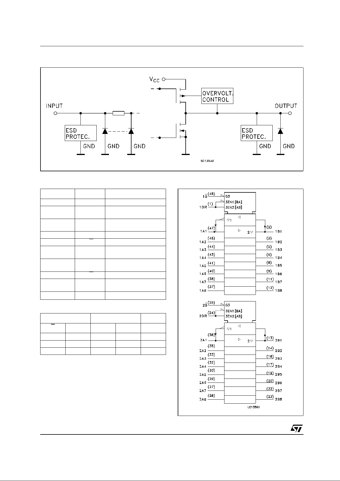
DESCRIPTION
The 74ALVCH16245 is a low voltage CMOS 16
BIT BUS TRANSCEIVER fabricated with
sub-micron silicon gate and five-layer metal wiring
C
2
MOS tec hnology. It is ideal for low p ower and
very high speed 1.65 to 3.6V applications; it can
be interfaced to 3.6V signal env ironment for both
inputs and outputs.
This IC is intended for two-way asynchronous
communication between data busses; the
direction of data transmission is determined by
DIR input. The enable input G
canbeusedto
disable the device so that the busses are
effectively isolated.
Bus hold on data inputs is prov ided in order to
eliminate the need for exte rnal pull-up or
pull-down resistor.
All inputs and outputs are equipped with
protection circuits against st atic discharge, giving
them 2KV ESD immunity and transient excess
voltage.
74ALVCH16245
LOW VOLTAGE CMOS 16-BIT TRANSCEIVER (3-STATE)
WITH 3.6V TOLERANT INPUTS AN D OUTPUTS
ORDER CODES
PACKAGE TUBE T & R
TSSOP 74ALVCH16245TTR
TSSOP
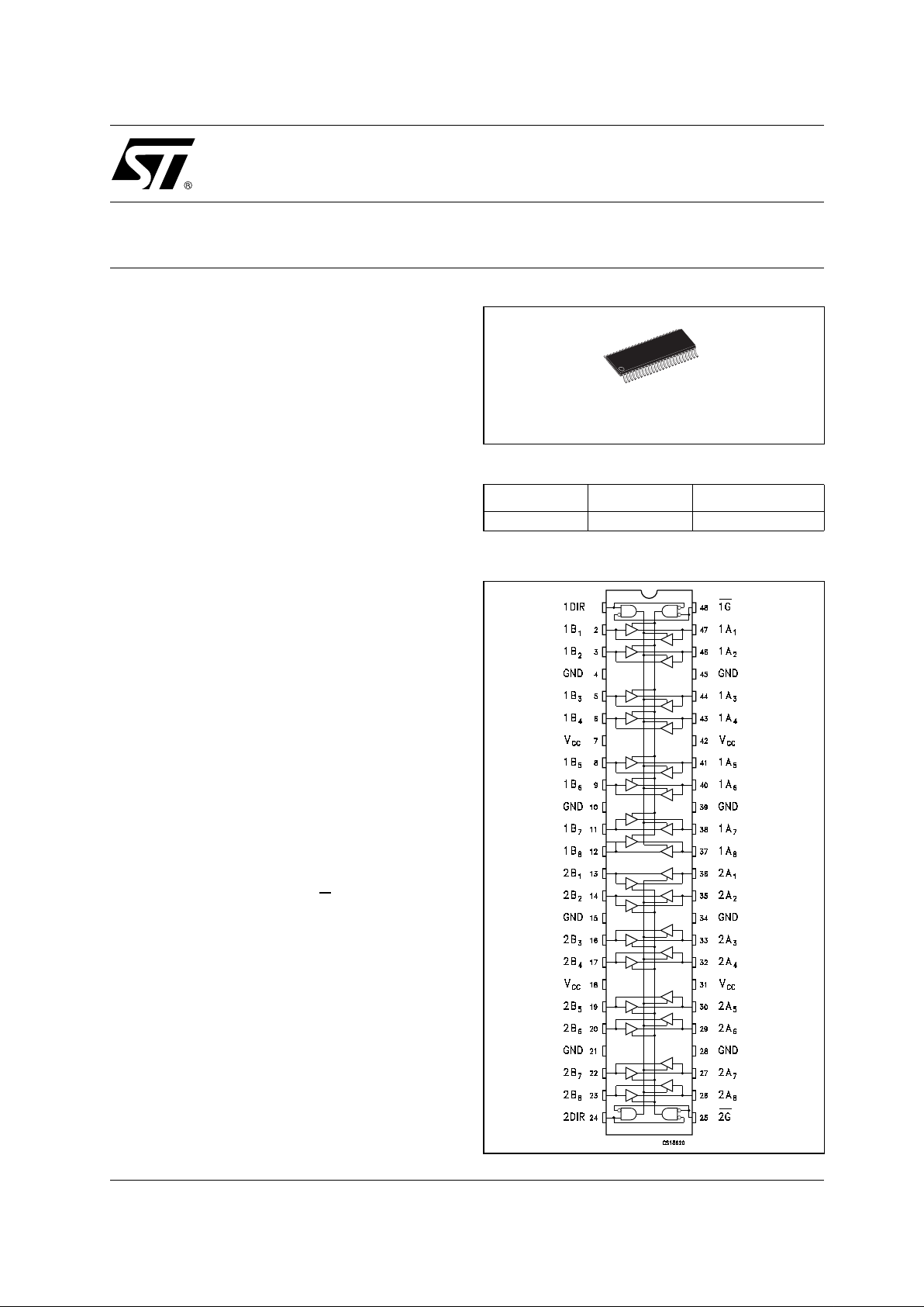
PIN CONNECTION
Page 2
74ALVCH16245
2/10
INPUT AND OUTPUT EQUIVALENT CIRCUIT
PIN DESCRIPTION
TRUTH TABLE
Z : High Impedance
X : Don‘tCare
IEC L OGIC SYMBOLS
PIN No SYMBOL NAME AND FUNCTION
1 1DIR Directional Control
2, 3, 5, 6, 8, 9,
11, 12
1B1 to 1B8 Data Inputs/Outputs
13,14,16,17,
19, 20, 22, 23
2B1 to 2B8 Data Inputs/Outputs
24 2DIR Directional Control
25 2G
Output Enable Input
36,35,33,32,
30, 29, 27, 26
2A1 to 2A8 Data Inputs/Outputs
47,46,44,43,
41, 40, 38, 38
1A1 to 1A8 Data Inputs/Outputs
48 1G
Output Enable Input
4, 10, 15, 21,
28, 34, 39, 45
GND Ground (0V)
7, 18, 31, 42
V
CC
Positive Supply Voltage
INPUTS FUNCTION OUTPUT
G
DIR A BUS B BUS Yn
L L OUTPUT INPUT A = B
L H INPUT OUTPUT B = A
HXZZZ
Page 3
74ALVCH16245
3/10
ABSOLUTE MAXIMUM RATINGS
Absolute Maximum Ratings are those values beyond which damage to the device may occur. Functional operation under these conditions is
not implied
1) I
O
absolute maximum rating must be observed
2) V
O
<GND,VO>V
CC
RECOMMENDED OPERATING CONDITIONS
1) VINfrom0.8V to 2V at VCC=3.0V
Symbol Parameter Value Unit
V
CC
Supply Voltage
-0.5 to +4.6 V
V
I
DC Input Voltage
-0.5 to +4.6 V
V
O
DC Output Voltage (OFF State)
-0.5 to +4.6 V
V
O
DC Output Voltage (High or Low State) (note 1) -0.5 to VCC+ 0.5
V
I
IK
DC Input Diode Current
-50 mA
I
OK
DC Output Diode Current (note 2)
-50 mA
I
O
DC Output Current
± 50 mA
I
CC
or I
GND
DC VCCor Ground Current per Supply Pin
± 100 mA
P
D
Power Dissipation
400 mW
T
stg
Storage Temperature
-65 to +150 °C
T
L
Lead Temperature (10 sec)
300 °C
Symbol Parameter Value Unit
V
CC
Supply Voltage
1.65 to 3.6 V
V
I
Input Voltage
-0.3 to 3.6 V
V
O
Output Voltage (OFF State)
0 to 3.6 V
V
O
Output Voltage (High or Low State) 0 to V
CC
V
I
OH,IOL
High or Low Level Output Current (VCC= 3.0 to 3.6V)
± 24 mA
I
OH,IOL
High or Low Level Output Current (VCC= 2.3 to 2.7V)
± 12 mA
I
OH,IOL
High or Low Level Output Current (VCC= 1.65V)
± 4mA
T
op
Operating Temperature
-55 to 125 °C
dt/dv Input Rise and Fall Time (note 1) 0 to 10 ns/V
Page 4

74ALVCH16245
4/10
DC SPECIFICATIONS
Symbol Parameter
Test Condition Value
Unit
V
CC
(V)
-40 to 85 °C -55 to 125 °C
Min. Max. Min. Max.
V
IH
High Level Input
Voltage
1.65 to 1.95 0.65 Vcc 0.65 Vcc
V
2.3 to 2.7 1.7 1.7
2.7 to 3.6 2.0 2.0
V
IL
Low Level Input
Voltage
1.65 to 1.95 0.35 Vcc 0.35 Vcc
2.3 to 2.7 0.7 0.7
2.7 to 3.6 0.8 0.8
V
OH
High Level Output
Voltage
1.65 to 3.6
IO=-100 µAVCC-0.2 VCC-0.2
V
1.65
I
O
=-4 mA
1.2 1.2
2.3
I
O
=-6 mA
2.0 2.0
2.3
I
O
=-12 mA
1.7 1.7
2.7
I
O
=-12 mA
2.2 2.2
3.0
I
O
=-12 mA
2.4 2.4
3.0
I
O
=-24 mA
2.0 2.0
V
OL
Low Level Output
Voltage
1.65 to 3.6
I
O
=100 µA
0.2 0.2 V
1.65
I
O
=4 mA
0.45 0.45
2.3
I
O
=6 mA
0.4 0.4
2.3
I
O
=12 mA
0.7 0.7
2.7
I
O
=12 mA
0.4 0.4
3.0
I
O
=24 mA
0.55 0.55
I
I
Input Leakage
Current
3.6
V
I
= 0 or 3.6V
± 5 ± 5 µA
I
IHOLD
Input Hold Current
1.65
VI=0.58 V
+25 +25
µA
1.65
V
I
=1.07 V
-25 -25
2.3
V
I
=0.7 V
+45 +45
2.3
V
I
=1.7 V
-45 -45
3.0
V
I
=0.8 V
+75 +75
3.0
V
I
=2 V
-75 -75
3.6
V
I
= 0 to 3.6V
± 500 ± 500
I
off
Power Off Leakage
Current
0V
I
or VO= 3.6V 10 20 µA
I
OZ
High Impedance
Output Leakage
Current
3.6 V
I=VIH
or V
IL
VO= 0 to V
CC
± 5 ± 10 µA
I
CC
Quiescent Supply
Current
3.6 VI=VCCor GND
I
O
=0
20 40 µA
∆I
CCICC
incr. per Input 3.0 to 3.6 VIH=VCC- 0.6V 500 750 µA
Page 5

74ALVCH16245
5/10
AC ELECTRICAL CHARACTERISTICS
1) Skew is defined as the absolute value of the difference between the actual propagation delay for any two outputs of the same device switching in the same direction, either HIGH or LOW (t
OSLH
=|t
PLHm-tPLHn
|, t
OSHL
=|t
PHLm-tPHLn
|)
2) Parameter guaranteed by design
CAPACITIVE CHARACTERISTICS
1) CPDis defined as the value of the IC’s internal equivalent capacitance which is calculated from the operating current consumption without
load. (Refer to Test Circuit). Average operating current can be obtained by the following equation. I
CC(opr)=CPDxVCCxfIN+ICC
/16 (per
circuit)
Symbol Parameter
Test Condition Value
Unit
V
CC
(V)
C
L
(pF)
R
L
(Ω)
t
s
= t
r
(ns)
-40 to 85 °C -55 to 125 °C
Min. Max. Min. Max.
t
PLHtPHL
Propagation Delay
Time
1.65 to 1.95 30 1000 2.0 1616
ns
2.3 to 2.7 30 500 2.0 1 3.7 1 3.7
2.7 50 500 2.5 1 3.6 1 3.6
3.0 to 3.6 50 500 2.5 1 3.0 1 3.0
t
PZLtPZH
Output Enable Time 1.65 to 1.95 30 1000 2.0 1 7.1 1 7.1
2.3 to 2.7 30 500 2.0 1 5.7 1 5.7
2.7 50 500 2.5 1 5.4 1 5.4
3.0 to 3.6 50 500 2.5 1 4.4 1 4.4
t
PLZtPHZ
Output Disable Time 1.65 to 1.95 30 1000 2.0 1 7.0 1 7.0
2.3 to 2.7 30 500 2.0 1 5.2 1 5.2
2.7 50 500 2.5 1 4.6 1 4.6
3.0 to 3.6 50 500 2.5 1 4.1 1 4.1
Symbol Parameter
Test Condition Value
Unit
V
CC
(V)
T
A
=25°C
Min. Typ. Max.
C
IN
Input Capacitance Control
Inputs
3.3
V
IN=VCC
or GND
4pF
C
I/O
Input Capacitance A or B ports
3.3
VIN=VCCor GND
8pF
C
PD
Power Dissipation Capacitance
Output enabled (note 1)
3.3 fIN= 10MHz
C
L
=50pF
V
IN
= 0 or V
CC
29
pF
2.5 22
C
PD
Power Dissipation Capacitance
Output disabled (note 1)
3.3 5
2.5 4
Page 6

74ALVCH16245
6/10
TEST CIRCUIT
RT=Z
OUT
of pulse generator (typically 50Ω)
TEST CIRCUIT AND WAVEFORM SYMBOL VALUE
TEST SWITCH
t
PLH,tPHL
Open
t
PZL,tPLZ(VCC
= 3.0 to 3.6V)
6V
t
PZL,tPLZ(VCC
= 2.3 to 2.7V) 2V
CC
t
PZH,tPHZ
GND
Symbol
V
CC
3.0 to 3.6V 2.7V 2.3 to 2.7V 1.65 to 1.95V
V
IH
2.7V 2.7V V
CC
V
CC
V
M
1.5V 1.5V VCC/2 VCC/2
V
X
VOL+0.3V VOL+0.3V VOL+0.15V VOL+0.15V
V
Y
VOH-0.3V VOH-0.3V VOH-0.15V VOH-0.15V
C
L
50pF 50pF 30pF 30pF
R
L=R1
500Ω 500Ω 500Ω 1000Ω
t
r=tr
<2.5ns <2.5ns <2.0ns <2.0ns
Page 7

74ALVCH16245
7/10
WAVEFORM 1: PROPAG ATION DE LAYS (f=1MHz; 50% duty cycle)
WAVEFORM 2: OUTPUT ENABLE AND DISABLE TIME (f=1MHz; 50% duty cycle)
Page 8

74ALVCH16245
8/10
DIM.
mm. inch
MIN. TYP MAX. MIN. TYP. MAX.
A 1.2 0.047
A1 0.05 0.15 0.002 0.006
A2 0.9 0.035
b 0.17 0.27 0.0067 0.011
c 0.09 0.20 0.0035 0.0079
D 12.4 12.6 0.488 0.496
E 8.1 BSC 0.318 BSC
E1 6.0 6.2 0.236 0.244
e 0 .5 BSC 0.0197 BSC
K0˚ 8˚0˚ 8˚
L 0.50 0.75 0.020 0.030
TSSOP48 MECHANICAL DATA
c
E
b
A2
A
E1
D
1
PIN 1 IDENTIFICATION
A1
L
K
e
7065588C
Page 9

74ALVCH16245
9/10
DIM.
mm. inch
MIN. TYP MAX. MIN. TYP. MAX.
A 330 12.992
C 12.8 13.2 0.504 0.519
D 20.2 0.795
N 60 2.362
T 30.4 1.197
Ao 8.7 8.9 0.343 0.350
Bo 13.1 13.3 0.516 0.524
Ko 1.5 1.7 0.059 0.067
Po 3.9 4.1 0.153 0.161
P 11.9 12.1 0.468 0.476
Tape & Reel TSSOP48 MECHANICAL DATA
Page 10

74ALVCH16245
10/10
Information furnished is believed to be accurate and reliable. H owever, STMicroelectronics assumes no responsibility for t he
consequences of use of such informatio n nor for any infringement of paten ts or o ther rig hts of t hird part ies which ma y result from
its use. No license is granted by implication or otherwise under any patent or patent rights of STMicroelectronics. Specifications
mentioned in this publicatio n are subject t o change without notice. This publication supersedes and replaces all in formation
previousl y suppl ied. STM icroel ectronics produc ts are not auth orized for use as c ritica l compone nts in l ife s upport dev ices or
systems without express written approval of STMicroelectronics.
© The ST logo is a registered trademark of STMicroelectronics
© 2002 STMicroelectronics - Printed in Italy - All Rights Reserved
STMicroelectronics GROUP OF COMPANIES
Australia - Brazil - Canada - China - Finland - France - Germany - Hong Kong - India - Israel - Italy - Japan - Malaysia - Malta - Morocc o
Singapore - Spain - Sweden - Switzerland - United Kingdom - United States.
© http://www.st.com
 Loading...