

Page 1
LOW VOLTAGE CMOS 16-BIT BUS BUFFER (3-STATE)
WITH 3.6V TOLERANT INPUTS AND OUTPUTS
■ 3.6V TOLERANT INPUTS AND OUTPUTS
■ HIGH SPEED :
t
= 3.9 ns (MAX.) at VCC=3.0to3.6V
PD
t
= 5.3 ns (MAX.) at VCC=2.3to2.7V
PD
t
= 7.5 ns (MAX.) at VCC=1.65V
PD
■ POWER DOWN PROTECTION ON INPUTS
AND OUTPUTS
■ SYMMETRICAL OUTPUT IMPEDANCE:
|=IOL= 24mA (MIN) at VCC=3.0V
|I
OH
|I
|=IOL= 18mA (MIN) at VCC=2.3V
OH
|I
|=IOL=4mA(MIN)atVCC= 1.65V
OH
■ OPERATING VOLTAGE RAN GE:
V
(OPR) = 1.65V to 3.6V
CC
■ BUS HOLD PROVIDED ON DATA INPUTS
■ PIN AND FUNCTION COMPATIBLE WITH
74 SERIES 16240
■ LATCH-UP PERFORMANCE EXCEEDS
300mA (JESD 17)
■ ESD PERFORMANCE:
HBM > 2000V (MIL STD 883 method 3015);
MM > 200V
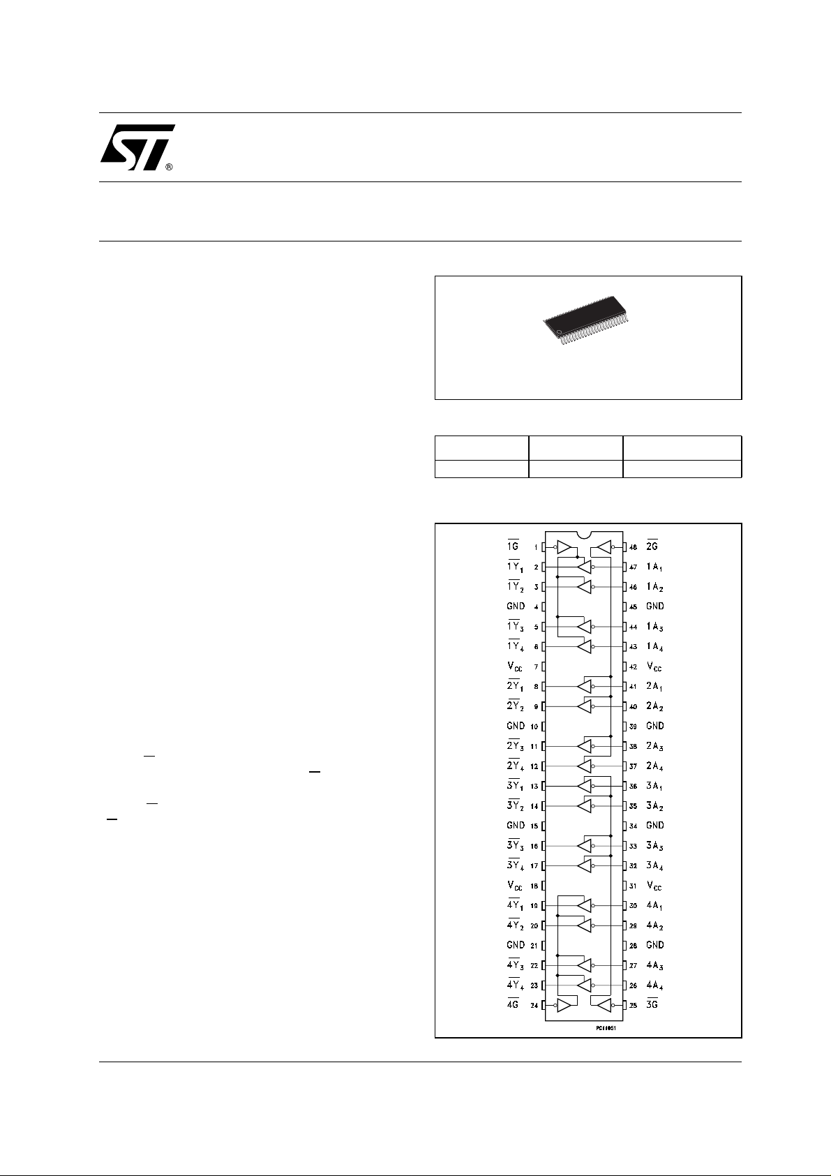
74ALVCH16240
TSSOP
ORDER CODES
PACKAGE TUBE T & R
TSSOP 74ALVCH16240TTR
PIN CO NNE CTION
DESCRIPTION
The 74ALVCH16240 is a low voltage CMOS 16
BIT BUS BUFFER (INVERTED) fabricated with
sub-micron silicon gate and five-layer metal wiring
2
C
MOS technology. It is ideal for low power and
very high speed 1.65 to 3.6V applications; it can
be interfaced to 3.6V s ignal environment for both
inputs and outputs.
Any nG
BUFFERS. Output Enable input (nG
output con trol governs four BUS
) tied together
gives full 16-bit operation.
When nG
nG
is LO W, the outputs are enabled. When
is HIGH, the output are in high impedance
state.
Active bus-hold circuitry is provided to hold
unused or floating data inputs at a valid logic level.
This device is designed to be used with 3 state
memory address drivers, etc.
All inputs and outputs are equipped with
protection circuits aga inst static discharge, giving
them 2KV ESD immunity and transient excess
voltage.
1/10February 2003
Page 2
74ALVCH16240
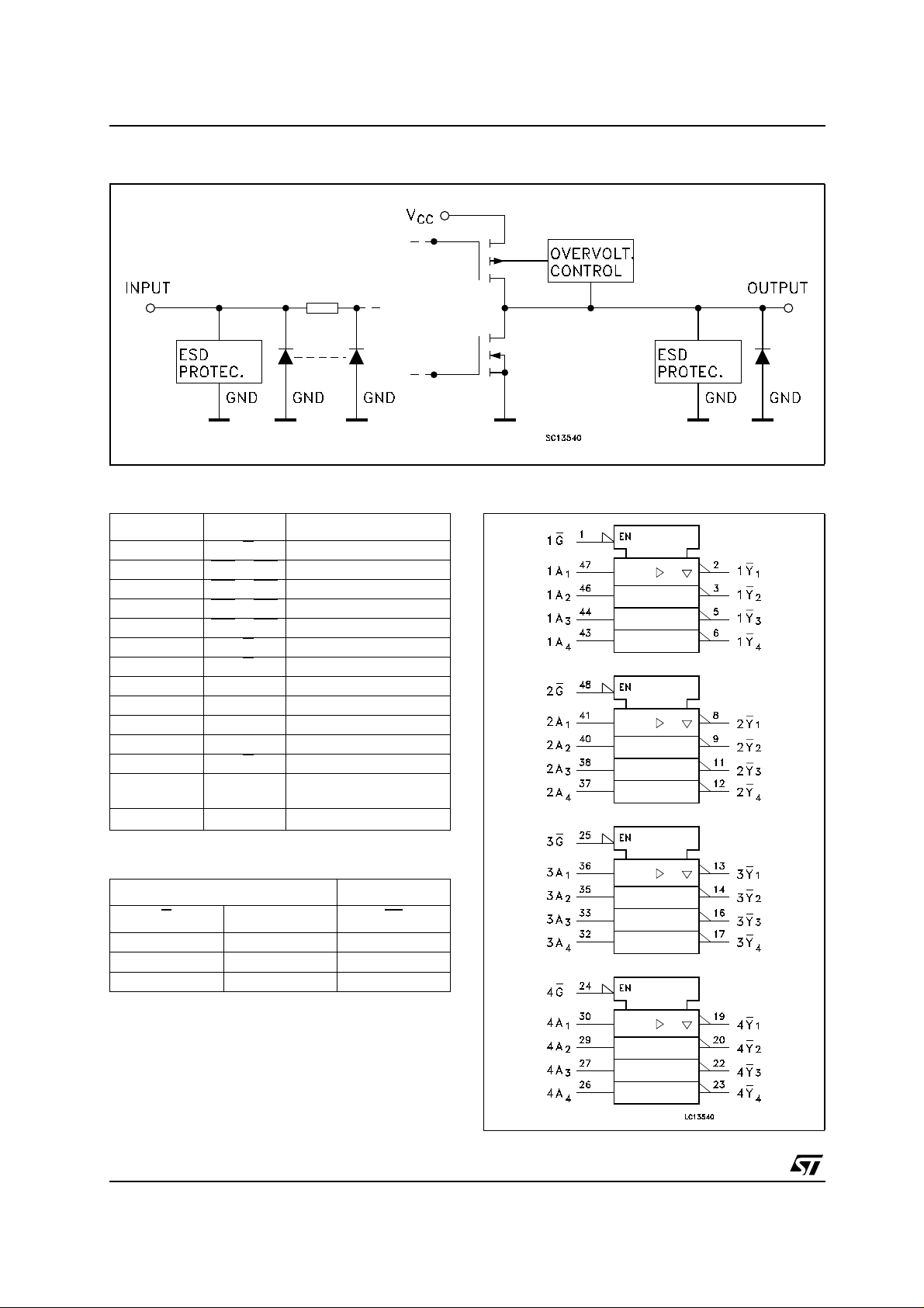
INPUT AND OUTPUT EQUIVALENT CIRCUIT
PIN DESCRIPTION
PIN No SYMBOL NAME AND FUNCTION
11G
2, 3, 5, 6 1Y1
8, 9, 11, 12 2Y1
13, 14, 16, 17 3Y1
19, 20, 22, 23 4Y1
24 4G
25 3G
30, 29, 27, 26 4A1 to 4A4 Data Outputs
36, 35, 33, 32 3A1 to 3A4 Data Outputs
41, 40, 38, 37 2A1 to 2A4 Data Outputs
47, 46, 44, 43 1A1 to 1A4 Data Outputs
48 2G
4, 10, 15, 21,
28, 34, 39, 45
7, 18, 31, 42
to 1Y4 Data Outputs
to 2Y4 Data Outputs
to 3Y4 Data Outputs
to 4Y4 Data Outputs
GND Ground (0V)
V
CC
Output Enable Input
Output Enable Input
Output Enable Input
Output Enable Input
Positive Supply Voltage
TRUTH TABLE
INPUTS OUTPUT
G
LLH
LHL
HXZ
X : Don‘t Care
Z : High Impedance
An Yn
IEC LOGIC SYMBOLS
2/10
Page 3
74ALVCH16240
ABSOLUTE MAXIMUM RATINGS
Symbol Parameter Value Unit
V
V
V
V
I
I
OK
I
or I
I
CC
P
T
T
Absolute Maximum Ratings are those values beyond which damage tothe device may occur. Functional operation under these conditions is
not implied
1) I
absolute maximum rating must be observed
O
2) V
<GND,VO>V
O
RECOMMENDED OPERATING CONDITIONS
Symbol Parameter Value Unit
V
V
V
V
I
OH,IOL
I
OH,IOL
I
OH,IOL
T
dt/dv Input Rise and Fall Time (note 1) 0 to 10 ns/V
1) VINfrom0.8V to 2Vat VCC=3.0V
Supply Voltage
CC
DC Input Voltage
I
DC Output Voltage (OFF State)
O
DC Output Voltage (High or Low State) (note 1) -0.5 to VCC+ 0.5
O
DC Input Diode Current
IK
DC Output Diode Current (note 2)
DC Output Current
O
DC VCCor Ground Current per Supply Pin
GND
Power Dissipation
D
Storage Temperature
stg
Lead Temperature (10 sec)
L
CC
Supply Voltage
CC
Input Voltage
I
Output Voltage (OFF State)
O
Output Voltage (High or Low State) 0 to V
O
High or Low Level Output Current (VCC= 3.0 to 3.6V)
High or Low Level Output Current (VCC= 2.3 to 2.7V)
High or Low Level Output Current (VCC= 1.8V)
Operating Temperature
op
-0.5 to +4.6 V
-0.5 to +4.6 V
-0.5 to +4.6 V
V
-50 mA
-50 mA
± 50 mA
± 100 mA
400 mW
-65 to +150 °C
300 °C
1.65 to 3.6 V
-0.3 to 3.6 V
0 to 3.6 V
CC
V
± 24 mA
± 12 mA
± 6mA
-55 to 125 °C
3/10
Page 4

74ALVCH16240
DC SPECIFICATIONS
Test Condition Value
Symbol Parameter
V
V
V
I
IHOLD
High Level Input
IH
Voltage
V
Low Level Input
IL
Voltage
High Level Output
OH
Voltage
Low Level Output
OL
Voltage
Input Leakage
I
I
Current
Bus Hold Input
Leakage Current
Power Off Leakage
I
off
Current
I
High Impedance
OZ
Output Leakage
Current
I
∆I
Quiescent Supply
CC
Current
CCICC
incr. per Input 3.0 to 3.6 VIH=VCC- 0.6V 500 750 µA
V
CC
(V)
-40 to 85 °C -55 to 125 °C
Min. Max. Min. Max.
1.65 to 1.95 0.65 Vcc 0.65 Vcc
2.3 to 2.7 1.7 1.7
2.7 to 3.6 2.0 2.0
1.65 to 1.95 0.35 Vcc 0.35 Vcc
2.3 to 2.7 0.7 0.7
2.7 to 3.6 0.8 0.8
1.65 to 3.6
1.65
2.3
2.3
2.7
3.0
3.0
1.65 to 3.6
1.65
2.3
2.3
2.7
3.0
3.6
1.65
1.65
2.3
2.3
3.0
3.0
3.6
0V
3.6 V
3.6 VI=VCCor GND
IO=-100 µAVCC-0.2 VCC-0.2
I
=-4 mA
O
=-6 mA
I
O
=-12 mA
I
O
=-12 mA
I
O
=-12 mA
I
O
=-24 mA
I
O
=100 µA
I
O
=4 mA
I
O
=6 mA
I
O
=12 mA
I
O
=12 mA
I
O
=24 mA
I
O
= 0 or 3.6V
V
I
VI=0.58 V
=1.07 V
V
I
=0.7 V
V
I
=1.7 V
V
I
=0.8 V
V
I
=2 V
V
I
= 0 to 3.6 V ± 500
V
I
or VO= 3.6V 10 20 µA
I
or V
I=VIH
VO= 0 to V
IL
CC
1.2 1.2
2.0 2.0
1.7 1.7
2.2 2.2
2.4 2.4
2.0 2.0
0.2 0.2
0.45 0.45
0.4 0.4
0.7 0.7
0.4 0.4
0.55 0.55
± 5 ± 5 µA
+25 +25
-25 -25
+45 +45
-45 -45
+75 +75
-75 -75
± 500
± 10 ± 10 µA
20 40 µA
I
=0
O
Unit
V
V
V
µA
4/10
Page 5

AC ELECTRICAL C HARACTERISTICS
Test Condition Value
74ALVCH16240
Symbol Parameter
t
PLHtPHL
Propagation Delay
Time
V
CC
(V)
C
(pF)
R
L
(Ω)
= t
t
L
s
(ns)
1.65 to 1.95 30 1000 2.0 1 7.5 1 7.5
2.3 to 2.7 30 500 2.0 1 5.3 1 5.3
-40 to 85 °C -55 to 125 °C
r
Min. Max. Min. Max.
Unit
2.7 50 500 2.5 1 5.3 1 5.3
3.0 to 3.6 50 500 2.5 1 3.9 1 3.9
t
PZLtPZH
Output Enable Time 1.65 to 1.95 30 1000 2.0 1 8.0 1 8.0
2.3 to 2.7 30 500 2.0 1 6.4 1 6.4
2.7 50 500 2.5 1 6.1 1 6.1
ns
3.0 to 3.6 50 500 2.5 1 5.0 1 5.0
t
PLZtPHZ
Output Disable Time 1.65 to 1.95 30 1000 2.0 1 7.5 1 7.5
2.3 to 2.7 30 500 2.0 1 5.4 1 5.4
2.7 50 500 2.5 1 4.8 1 4.8
3.0 to 3.6 50 500 2.5 1 4.4 1 4.4
1) Skew isdefined astheabsolute value ofthedifference betweentheactual propagation delay for any twooutputs ofthesamedevice switching in the same direction, either HIGH or LOW (t
2) Parameter guaranteed by design
OSLH
=|t
PLHm-tPLHn
|, t
OSHL
=|t
PHLm-tPHLn
|)
CAPACITIVE CHARACTERISTICS
Test Condition Value
=25°C
Symbol Parameter
V
CC
(V)
C
C
C
OUT
C
C
1) CPDis defined as the value of the IC’s internal equivalent capacitance which is calculated from the operating current consumption without
load. (Refer to Test Circuit). Average operating current can be obtained by the following equation. I
circuit)
Input Capacitance Control
IN
Inputs
Input Capacitance Data Inputs
IN
Output Capacitance
Power Dissipation Capacitance
PD
Output enabled (note 1)
Power Dissipation Capacitance
PD
Output disabled (note 1)
3.3
3.3
3.3
V
IN=VCC
VIN=VCCor GND
VIN= 0 to V
or GND
CC
3.3 fIN= 10MHz
C
V
IN
=50pF
L
= 0 or V
CC
2.5 16
3.3 5
2.5 4
T
A
Min. Typ. Max.
3pF
6pF
7pF
19
CC(opr)=CPDxVCCxfIN+ICC
Unit
pF
/16 (per
5/10
Page 6

74ALVCH16240
TEST CIRCUIT
TEST SWITCH
t
PLH,tPHL
t
PZL,tPLZ(VCC
t
PZL,tPLZ(VCC
t
PZH,tPHZ
RT=Z
OUT
TEST CIRCUIT AND WAVE FORM SYMBOL VALUE
= 3.0 to 3.6V)
= 2.3 to 2.7V) 2V
of pulse generator (typically 50Ω)
Open
6V
CC
GND
Symbol
V
IH
V
M
V
X
V
Y
C
L
R
L=R1
t
r=tr
V
CC
3.0 to 3.6V 2.7V 2.3 to 2.7V 1.65 to 1.95V
2.7V 2.7V V
CC
V
CC
1.5V 1.5V VCC/2 VCC/2
VOL+0.3V VOL+0.3V VOL+0.15V VOL+0.15V
VOH-0.3V VOH-0.3V VOH-0.15V VOH-0.15V
50pF 50pF 30pF 30pF
500Ω 500Ω 500Ω 1000Ω
<2.5ns <2.5ns <2.0ns <2.0ns
6/10
Page 7

WAVEFORM 1 : PROPAGATION DEL AYS (f=1MHz; 50% duty cycle)
WAVEFORM 2 : OUTPUT ENABL E AND DISABLE TIME (f=1MHz; 50% duty cycle)
74ALVCH16240
7/10
Page 8

74ALVCH16240
TSSOP48 MECHANICAL DATA
mm. inch
DIM.
MIN. TYP MAX. MIN. TYP. MAX.
A 1.2 0.047
A1 0.05 0.15 0.002 0.006
A2 0.9 0.035
b 0.17 0.27 0.0067 0.011
c 0.09 0.20 0.0035 0.0079
D 12.4 12.6 0.488 0.496
E 8.1 BSC 0.318 BSC
E1 6. 0 6.2 0.236 0.244
e 0 .5 BSC 0.0197 BSC
K0˚ 8˚0˚ 8˚
L 0.50 0.75 0. 020 0.030
A2
A
A1
b
e
D
K
c
E1
L
E
PIN 1 IDENTIFICATION
8/10
1
7065588C
Page 9

74ALVCH16240
Tape & Reel TSSOP48 MECHANICAL DATA
mm. inch
DIM.
MIN. TYP MAX. MIN. TYP. MAX.
A 330 12.992
C 12.8 13.2 0.504 0.519
D 20.2 0.795
N 60 2.362
T 30.4 1.197
Ao 8.7 8.9 0.343 0.350
Bo 13.1 13.3 0.516 0.524
Ko 1.5 1.7 0.059 0.067
Po 3.9 4.1 0.153 0.161
P 11.9 12.1 0.468 0.476
9/10
Page 10

74ALVCH16240
Information furnished is believed to be accurate and reliable. However, STMicroelectronics assumes no responsibilit y for the
consequences of use of such informatio n nor for any infringement of paten ts or o ther rig hts of t hird part ies which ma y result from
its use. No license is granted by implication or otherwise under any patent or patent rights of STMicroelectronics. Specifications
mentioned in this publication are subject to change without notice. This publication supersedes and replaces all information
previousl y suppl ied. STM icroel ectronics produc ts are not auth orized for use as c ritica l compone nts in l ife s upport dev ices or
systems without express written approval of STMicroelectronics.
Australia - Brazil - Canada - China - Finland - France - Germany - Hong Kong - India - Israel - Italy - Japan - Malaysia - Malta - Morocco
© The ST logo is a registered trademark of STMicroelectronics
© 2002 STMicroelectronics - Printed in Italy - All Rights Reserved
STMicroelectronics GROUP OF COMPANIES
Singapore - Spain - Sweden - Switzerland - United Kingdom - United States.
© http://www.st.com
10/10
 Loading...