

Page 1
INTEGRATED CIRCUITS
74ALS74A
Dual D-type flip-flop with set and reset
Product specification 1996 Jul 01
IC05 Data Handbook
Page 2
Philips Semiconductors Product specification
74ALS74ADual D-type flip-flop with set and reset
DESCRIPTION
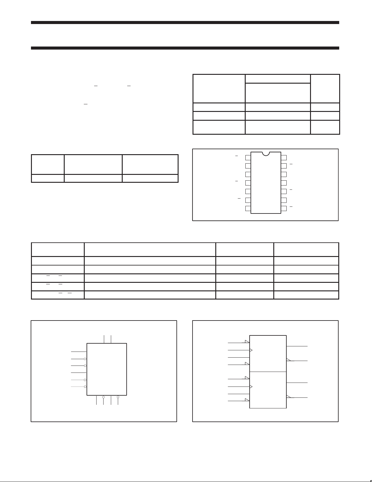
The 74ALS74 is a dual positive edge-triggered D-type flip-flop
featuring individual data, clock, set, and reset inputs; also true and
complementary outputs. Set (S
active-Low inputs and operate independently of the clock input.
When set and reset are inactive (High), data at the D input is
transferred to the Q and Q
the clock. Data must be stable just one setup time prior to the
Low-to-High transition of the clock for predictable operation. Clock
triggering occurs at a voltage level and is not directly related to the
transition time of the positive-going pulse. Following the hold time
D) and reset (RD) are asynchronous
outputs on the Low-to-High transition of
ORDERING INFORMATION
ORDER CODE
DESCRIPTION COMMERCIAL RANGE
14-pin plastic DIP 74ALS74AN SOT27-1
14-pin plastic SO 74ALS74AD SOT108-1
14-pin plastic SSOP
Type II
= 5V ±10%,
V
CC
T
= 0°C to +70°C
amb
74ALS74ADB SOT337-1
interval, data at the D input may be changed without affecting the
levels of the output.
TYPE
TYPICAL f
MAX
SUPPLY CURRENT
74ALS74A 150MHz 3.0mA
TYPICAL
(TOTAL)
PIN CONFIGURATION
1
D0
R
2
D0
CP0
3
D0
S
4
Q0
5
Q
0
6
GND
14
13
12
11
10
9
87
SF00045
V
R
D1
CP1
SD1
Q1
Q1
CC
D1
INPUT AND OUTPUT LOADING AND FAN-OUT TABLE
PINS DESCRIPTION
74ALS (U.L.)
HIGH/LOW
D0, D1 Data inputs 1.0/2.0 20µA/0.2mA
CP0, CP1 Clock inputs (active rising edge) 1.0/2.0 20µA/0.2mA
SD0, SD1 Set inputs (active-Low) 2.0/4.0 40µA/0.4mA
RD0, RD1 Reset inputs (active-Low) 2.0/4.0 40µA/0.4mA
Q0, Q1, Q0, Q1 Data outputs 20/80 0.4mA/8mA
NOTE: One (1.0) ALS unit load is defined as: 20µA in the High state and 0.1mA in the Low state.
LOAD VALUE
HIGH/LOW
DRAWING
NUMBER
LOGIC SYMBOL
212
3
4
1
11
10
13
VCC = Pin 14
GND = Pin 7
1996 Jul 01 853–1278 01670
D0 D1
CP0
SD0
RD0
CP1
SD1
RD1
Q0 Q0 Q1 Q1
56 98
SF00046
IEC/IEEE SYMBOL
2
4
3
2
1
10
11
12
13
&
S
C1
1D
R
S
C2
2D
R
5
6
9
8
SF00047
Page 3
Philips Semiconductors Product specification
SYMBOL
PARAMETER
UNIT
74ALS74ADual D-type flip-flop with set and reset
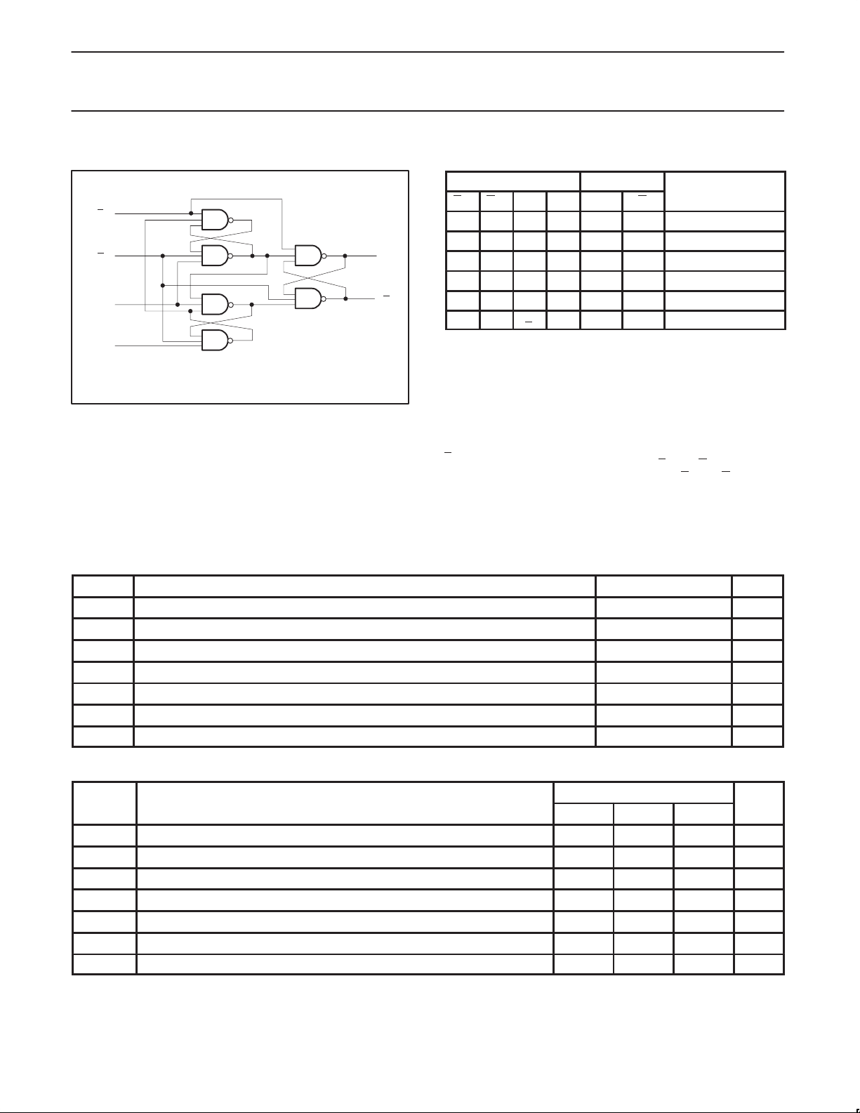
LOGIC DIAGRAM
FUNCTION TABLE
INPUTS OUTPUTS OPERATING
4, 10
S
D
1, 13
D
R
5, 9
Q
SD RD CP D Q Q MODE
L H X X H L Asynchronous set
H L X X L H Asynchronous reset
L L X X H H Undetermined*
H H ↑ h H L Load “1”
6, 8
CP
3, 11
Q
H H ↑ l L H Load “0”
H H ↑ X NC NC Hold
D
VCC = Pin 14
GND = Pin 7
2, 12
SF00048
H = High voltage level
h = High state must be present one setup time prior to
Low-to-High clock transition
L = Low voltage level
l = Low state must be present one setup time prior to
Low-to-High clock transition
NC= No change from the previous setup
X = Don’t care
↑ = Low-to-High clock transition
= Not Low-to-High clock transition
↑
* = Both outputs will be High while both S
but the output states are unpredictable if S
High simultaneously
ABSOLUTE MAXIMUM RATINGS
(Operation beyond the limit set forth in this table may impair the useful life of the device.
Unless otherwise noted these limits are over the operating free-air temperature range.)
SYMBOL
V
CC
V
IN
I
IN
V
OUT
I
OUT
T
amb
T
stg
Supply voltage –0.5 to +7.0 V
Input voltage –0.5 to +7.0 V
Input current –30 to +5 mA
Voltage applied to output in High output state –0.5 to V
Current applied to output in Low output state 16 mA
Operating free-air temperature range 0 to +70 °C
Storage temperature range –65 to +150 °C
PARAMETER RATING UNIT
D and RD are Low,
D and RD go
CC
V
RECOMMENDED OPERATING CONDITIONS
V
V
V
I
OH
I
OL
T
amb
1996 Jul 01
Supply voltage 4.5 5.0 5.5 V
CC
High-level input voltage 2.0 V
IH
Low-level input voltage 0.8 V
IL
I
Input clamp current –18 mA
Ik
High-level output current –0.4 mA
Low-level output current
Operating free-air temperature range 0 +70 °C
LIMITS
MIN NOM MAX
8 mA
3
Page 4
Philips Semiconductors Product specification
SYMBOL
PARAMETER
TEST CONDITIONS
1
UNIT
VOLLow-level output voltage
CC
,
IL
,
I
V
MAX, V
0V
IIHHigh–level input current
V
MAX, V
7V
IILLow–level input current
V
MAX, V
4V
74ALS74ADual D-type flip-flop with set and reset
DC ELECTRICAL CHARACTERISTICS
(Over recommended operating free-air temperature range unless otherwise noted.)
LIMITS
MIN TYP
V
High-level output voltage
OH
p
V
I
I
CC
Input clamp voltage VCC = MIN, II = I
IK
Input current at maximum input
I
voltage
p
Output current
O
Supply current (total)
p
3
4
Dn, CPn
SDn, RDn
Dn, CPn
SDn, RDn
Dn, CPn
SDn, RDn
VCC = ±10%,
V
= MAX, VIH = MIN
IL
VCC = MIN, VIL = MAX,
VIH = MIN
IK
CC
CC
CC
=
=
=
= 7.
I
= 2.
I
= 0.
I
IOH = MAX V
I
= 4mA 0.25 0.40 V
OL
I
= 8mA 0.35 0.50 V
OL
VCC = MAX, VO = 2.25V –30 –112 mA
VCC = MAX 3.0 4.0 mA
– 2 V
CC
NOTES:
1. For conditions shown as MIN or MAX, use the appropriate value specified under recommended operating conditions for the applicable type.
2. All typical values are at V
3. The output conditions have been chosen to produce a current that closely approximates one half of the true short–circuit output current, I
4. Measure I
with the Dn, CPn, and SDn grounded, then with Dn, CPn, and RDn grounded.
CC
= 5V, T
CC
amb
= 25°C.
2
MAX
–0.73 –1.5 V
0.1 mA
0.2 mA
20 µA
40 µA
–0.2 mA
–0.4 mA
OS
.
AC ELECTRICAL CHARACTERISTICS
LIMITS
T
= 0°C to +70°C
amb
= +5.0V ± 10%
SYMBOL PARAMETER TEST CONDITION
V
CC
= 50pF, RL = 500Ω
C
L
MIN MAX
f
max
t
PLH
t
PHL
t
PLH
t
PHL
Maximum clock frequency Waveform 1 80 MHz
Propagation delay
CPn to Qn or Q
n
Propagation delay
S
Dn or RD to Qn or Qn
Waveform 1
Waveform 2, 3
3.0
3.0
1.0
3.0
14.0
14.0
10.0
AC SETUP REQUIREMENTS
LIMITS
T
= 0°C to +70°C
amb
= +5.0V ± 10%
SYMBOL PARAMETER TEST CONDITION
t
(H)
su
t
su
t
(H)
h
t
(L)
h
t
w
t
w
t
w
t
rec
Setup time, High or Low
Dn to CPn
(L)
Hold time, High or Low
Dn to CPn
(H)
CPn Pulse width
High or Low
(L)
Waveform 1
Waveform 1
Waveform 1
(L) SDn or RDn Pulse width, Low Waveform 2, 3 6.0 ns
Recovery time, SDn or RDn to CPn Waveform 2, 3 6.0 ns
V
CC
= 50pF, RL = 500Ω
C
L
MIN MAX
6.0
6.0
0.0
0.0
6.0
6.0
8.0
UNIT
ns
ns
UNIT
ns
ns
ns
1996 Jul 01
4
Page 5
Philips Semiconductors Product specification
74ALS74ADual D-type flip-flop with set and reset
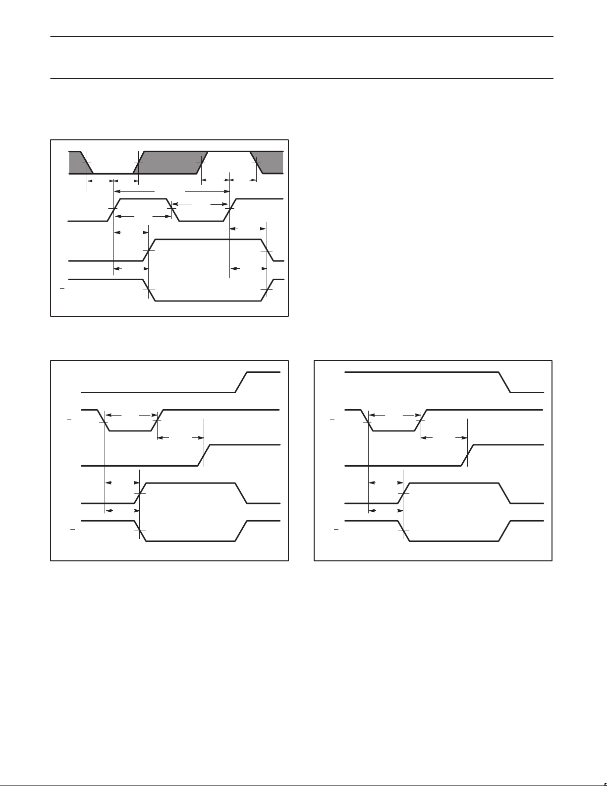
AC WAVEFORMS
For all waveforms, VM = 1.3V.
The shaded areas indicate when the input is permitted to change for predictable output performance.
Dn
CPn
Qn
Qn
V
M
tsu(L) th(L)
V
M
V
t
t
M
PLH
PHL
tw(H)
V
M
tsu(H) th(H)
1/f
max
(L)
t
V
M
V
M
V
M
w
Waveform 1. Propagation Delay for Data to Output,
Data Setup and Hold Times, Clock Width,
and Maximum Clock Frequency
Dn
SDn
CPn
V
M
tw(L)
V
M
t
REC
V
M
V
M
V
M
t
PHL
V
M
t
PLH
V
M
SF00049
Dn
RDn
CPn
V
M
tw(L)
V
M
t
REC
V
M
t
Qn
Qn
PLH
t
PHL
V
M
V
M
Waveform 2. Propagation Delay for Set to Output,
Set Pulse Width and Recovery Time for Set to Clock
1996 Jul 01
SC00040
t
Qn
Qn
PLH
t
PHL
V
M
V
M
Waveform 3. Propagation Delay for Reset to Output,
Reset Pulse Width and Recovery Time for Reset to Clock
5
SC00041
Page 6
Philips Semiconductors Product specification
74ALS74ADual D-type flip-flop with set and reset
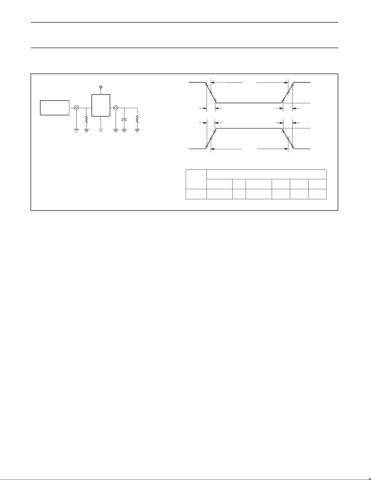
TEST CIRCUIT AND WAVEFORMS
V
CC
PULSE
GENERATOR
V
IN
R
T
D.U.T.
V
OUT
C
R
L
L
Test Circuit for Totem-pole Outputs
DEFINITIONS:
R
= Load resistor;
L
see AC electrical characteristics for value.
C
= Load capacitance includes jig and probe capacitance;
L
see AC electrical characteristics for value.
= Termination resistance should be equal to Z
R
T
pulse generators.
OUT
of
NEGATIVE
PULSE
POSITIVE
PULSE
Family
74ALS
90%
10%
V
M
10%
t
THL (tf
t
TLH (tr
90%
V
M
Input Pulse Definition
Amplitude
3.5V
t
w
10%
)
f
)
t
w
t
TLH (tr
t
THL (tf
)
)
90%
90%
V
M
V
M
10%
INPUT PULSE REQUIREMENTS
V
M
1.3V
Rep.Rate
1MHz
500ns
t
w
t
TLHtTHL
2.0ns 2.0ns
AMP (V)
0.3V
AMP (V)
0.3V
SC00005
1996 Jul 01
6
Page 7
Philips Semiconductors Product specification
74ALS74ADual D-type flip-flop with set and reset
DEFINITIONS
Data Sheet Identification Product Status Definition
Objective Specification
Preliminary Specification
Product Specification
Formative or in Design
Preproduction Product
Full Production
Philips Semiconductors and Philips Electronics North America Corporation reserve the right to make changes, without notice, in the products,
including circuits, standard cells, and/or software, described or contained herein in order to improve design and/or performance. Philips
Semiconductors assumes no responsibility or liability for the use of any of these products, conveys no license or title under any patent, copyright,
or mask work right to these products, and makes no representations or warranties that these products are free from patent, copyright, or mask
work right infringement, unless otherwise specified. Applications that are described herein for any of these products are for illustrative purposes
only. Philips Semiconductors makes no representation or warranty that such applications will be suitable for the specified use without further testing
or modification.
LIFE SUPPORT APPLICA TIONS
Philips Semiconductors and Philips Electronics North America Corporation Products are not designed for use in life support appliances, devices,
or systems where malfunction of a Philips Semiconductors and Philips Electronics North America Corporation Product can reasonably be expected
to result in a personal injury. Philips Semiconductors and Philips Electronics North America Corporation customers using or selling Philips
Semiconductors and Philips Electronics North America Corporation Products for use in such applications do so at their own risk and agree to fully
indemnify Philips Semiconductors and Philips Electronics North America Corporation for any damages resulting from such improper use or sale.
Philips Semiconductors
811 East Arques Avenue
P.O. Box 3409
Sunnyvale, California 94088–3409
Telephone 800-234-7381
This data sheet contains the design target or goal specifications for product development. Specifications
may change in any manner without notice.
This data sheet contains preliminary data, and supplementary data will be published at a later date. Philips
Semiconductors reserves the right to make changes at any time without notice in order to improve design
and supply the best possible product.
This data sheet contains Final Specifications. Philips Semiconductors reserves the right to make changes
at any time without notice, in order to improve design and supply the best possible product.
Copyright Philips Electronics North America Corporation 1997
All rights reserved. Printed in U.S.A.
1991 Jul 01
7
Page 8

Philips Semiconductors Product specification
74ALS74ADual D-type flip-flop with set and reset
DIP14: plastic dual in-line package; 14 leads (300 mil) SOT27-1
1996 Jul 01
8
Page 9

Philips Semiconductors Product specification
74ALS74ADual D-type flip-flop with set and reset
SO14: plastic small outline package; 14 leads; body width 3.9 mm SOT108-1
1996 Jul 01
9
Page 10

Philips Semiconductors Product specification
74ALS74ADual D-type flip-flop with set and reset
NOTES
1996 Jul 01
10
 Loading...