

Datasheet 74ACT843SPC, 74ACT843SCX, 74ACT843SC, 74ACT843CW Datasheet (Fairchild Semiconductor)
Page 1
© 2000 Fairchild Semiconductor Corporation DS009800 www.fairchildsemi.com
July 1988
Revised September 2000
74ACT843 9-Bit Transparent Latch
74ACT843
9-Bit Transparent Latch
General Description
The ACT843 bus inter face latch is designed to e liminate
the extra packages required to buffer existing latch es and
provide extra data width for wider address/data paths.
Features
■ TTL compatible inputs
■ 3-STATE outputs for bus interfacing
Ordering Code:
Device also available in Tape and Reel. Specify by appending s uffix let te r “X” to the ordering code. (SPC not available in Tape and Reel.)
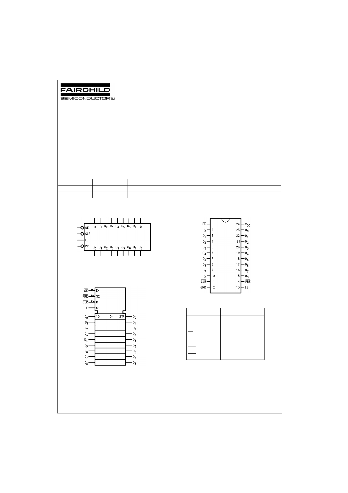
Logic Symbols
IEEE/IEC
Connection Diagram
Pin Descriptions
FACT is a trademark of Fairchild Semiconductor Corporation
Order Number Package Number Package Description
74ACT843SC M24B 24-Lead Small Outline Integrated Circuit (SOIC), JEDEC MS-013, 0.300 Wide
74ACT843SPC N24C 24-Lead Plastic Dual-In-Line Package (PDIP), JEDEC MS-001, 0.300 Wide
Pin Names Description
D
0–D8
Data Inputs
O
0–O8
Data Outputs
OE
Output Enable
LE Latch Enable
CLR
Clear
PRE
Preset
Page 2
www.fairchildsemi.com 2
74ACT843
Functional Description
The ACT843 consists of nine D-t ype latches with 3 -STATE
outputs. The flip-flops a ppe ar tran spa ren t to th e da ta w he n
Latch Enable (LE) is HIGH. This allows asynchronous
operation, as the output transition follows the data in transition. On the LE HIGH-to-LOW transition, the data that
meets the setup times is latched. Data appears on the bus
when the Output Enabl e (OE
) is LOW. When OE is HIGH,
the bus output is in the high impedance state. In addition to
the LE and OE
pins, the ACT843 has a Clear (CLR) pin
and a Preset (PRE
) pin. These pins are idea l f or p ari t y bus
interfacing in high performance systems. When CLR
is
LOW, the outputs are LOW if OE
is LOW. When CLR is
HIGH, data can be entere d into the latch. When PRE
is
LOW, the outputs are HIGH if OE
is LOW. Preset overrides
CLR
.
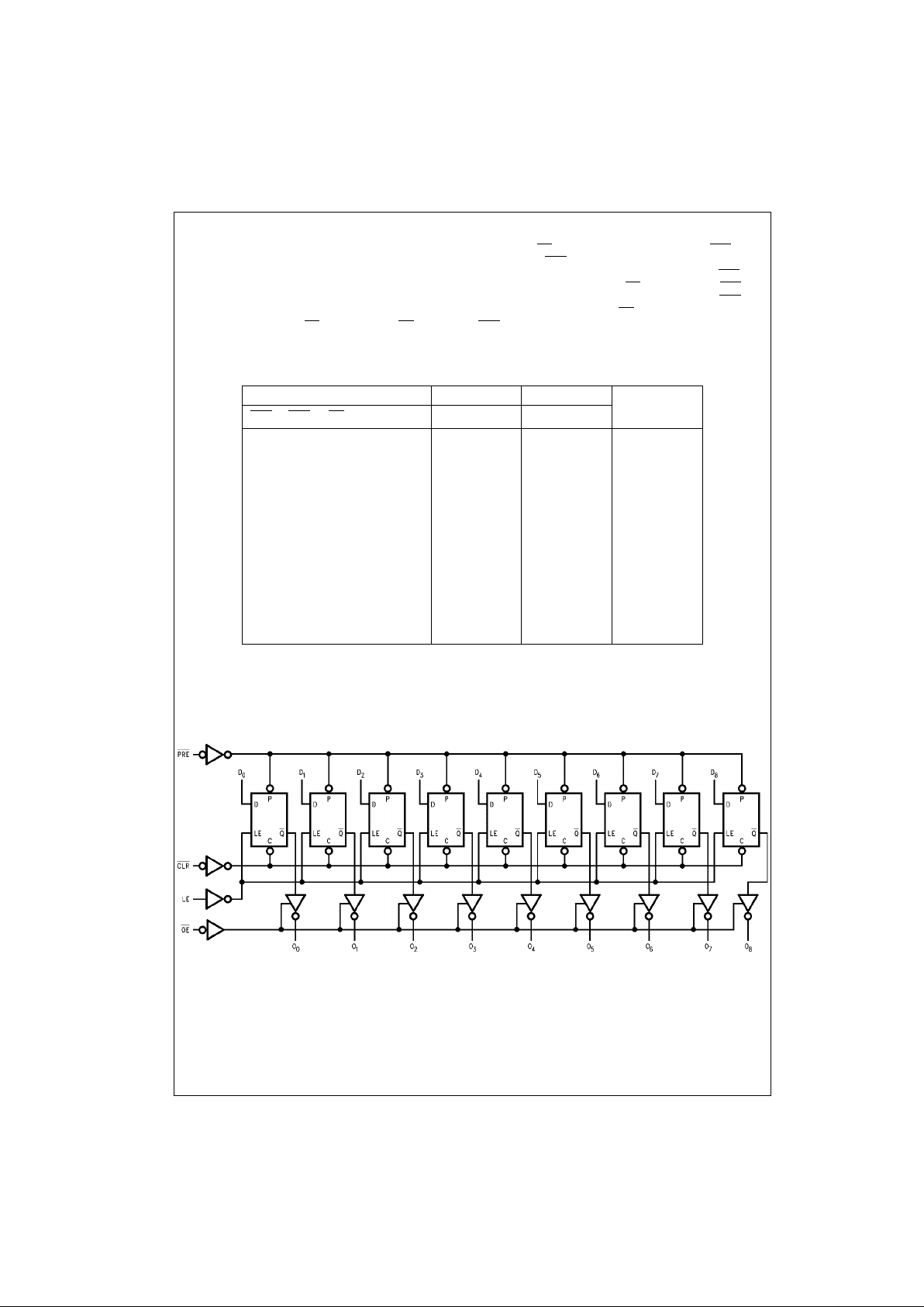
Function Tables
H = HIGH Voltage Level
L = LOW Voltage Level
X = Immaterial
Z = High Impedance
NC = No Change
Logic Diagram
Inputs Internal Outputs
Function
CLR
PRE OE LE D Q O
HHHHL L Z High Z
HHHHH H Z High Z
H H H L X NC Z Latched
H H L H L L L Transparent
H H L H H H H Transparent
H H L L X NC NC Latched
H L L X X H H Preset
L H L X X L L Clear
LLLXX H H Preset
L H H L X L Z Clear/High Z
H L H L X H Z Preset/High Z
Page 3

3 www.fairchildsemi.com
74ACT843
Absolute Maximum Ratings(Note 1) Recommended Operating
Conditions
Note 1: Absolute max imum ratings are t hose values bey ond which damage
to the device may occu r. The databook spe cificatio ns shou ld be met, wit hout exception, to ensure that the system de sign is relia ble over its p ower
supply, temperature, and output/input loading variables. Fairchild does not
recommend operation of FACT circuits outside databook specificatio ns .
DC Electrical Characteristics
Note 2: All outputs loaded; thres holds on input associate d w it h output under test.
Note 3: Maximum test duration 2.0 ms, one output loaded at a time.
Supply Voltage (VCC) −0.5V to +7.0V
DC Input Diode Current (I
IK
)
V
I
= −0.5V −20 mA
V
I
= VCC +0.5V +20 mA
DC Input Voltage (V
I
) −0.5V to VCC +0.5V
DC Output Diode Current (I
OK
)
V
O
= −0.5V −20 mA
V
O
= VCC +0.5V +20 mA
DC Output Voltage (V
O
) −0.5V to VCC +0.5V
DC Output Source
or Sink Current (I
O
) ±50 mA
DC V
CC
or Ground Current
per Output Pin (I
CC
or I
GND
) ±50 mA
Storage Temperature (T
STG
) −65°C to +150°C
Junction Temperature (T
J
)
PDIP 140
°C
Supply Voltage (V
CC
) 4.5V to 5.5V
Input Voltage (V
I
)0V to V
CC
Output Voltage (VO)0V to V
CC
Operating Temperature (TA) −40°C to +85°C
Minimum Input Edge Rate (
∆V/∆t) 125 mV/ns
V
IN
from 0.8V to 2.0V
V
CC
@ 4.5V, 5.5V
Symbol Parameter
V
CC
TA = +25°CT
A
= −40°C to +85°C
Units Conditions
(V) Typ Guaranteed Limits
V
IH
Minimum HIGH Level 4.5 1.5 2.0 2.0
V
V
OUT
= 0.1V
Input Voltage 5.5 1.5 2.0 2.0 or VCC − 0.1V
V
IL
Maximum LOW Level 4.5 1.5 0.8 0.8
V
V
OUT
= 0.1V
Input Voltage 5.5 1.5 0.8 0.8 or VCC − 0.1V
V
OH
Minimum HIGH Level 4.5 4.49 4.4 4.4
VI
OUT
= −50 µA
Output Voltage 5.5 5.49 5.4 5.4
VIN = V
IL
or V
IH
4.5 3.86 3.76 V IOH = −24 mA
5.5 4.86 4.76 IOH = −24 mA (Note 2)
V
OL
Maximum LOW Level 4.5 0.001 0.1 0.1
VI
OUT
= 50 µA
Output Voltage 5.5 0.001 0.1 0.1
VIN = V
IL
or V
IH
4.5 0.36 0.44 V IO = 24 mA
5.5 0.36 0.44 I
OL
= 24 mA (Note 2)
I
IN
Maximum Input
5.5 ±0.1 ±1.0 µAV
I
= VCC, GND
Leakage Current
I
OZ
Maximum 3- STATE
5.5 ±0.5 ±5.0 µA
VI = VIL, V
IH
Leakage Current VO = VCC, GND
I
CCT
Maximum
5.5 0.6 1.5 mA VI = VCC − 2.1V
ICC/Input
I
OLD
Minimum Dynamic 5.5 75 mA V
OLD
= 1.65V Max
I
OHD
Output Current (Note 3) 5.5 −75 mA V
OHD
= 3.85V Min
I
CC
Maximum Quiescent
5.5 8.0 80.0 µA
VIN = V
CC
Supply Current or GND
Page 4

www.fairchildsemi.com 4
74ACT843
AC Electrical Characteristics
Note 4: Voltage Range 5.0 is 5.0V ± 0.5V
AC Operating Requirements
Note 5: Voltage Range 5.0 is 5.0V ± 0.5V
Capacitance
V
CC
TA = +25°CT
A
= −40°C to +85°C
Symbol Parameter (V)
C
L
= 50 pF CL = 50 pF
Units
(Note 4) Min Typ Max Min Max
t
PLH
Propagation Delay
5.0 2.5 5.5 9.5 2.0 10.0 ns
D
n
to O
n
t
PHL
Propagation Delay
5.0 2.5 5.5 9.5 2.0 10.0 ns
D
n
to O
n
t
PLH
Propagation Delay
5.0 2.5 5.5 9.0 2.0 10.0 ns
LE to O
n
t
PHL
Propagation Delay
5.0 2.5 5.5 9.0 2.0 10.0 ns
LE to O
n
t
PLH
Propagation Delay
5.0 2.5 6.5 14.0 2.0 16.0 ns
PRE
to O
n
t
PHL
Propagation Delay
5.0 2.5 7.5 15.5 2.0 17.5 ns
CLR to O
n
t
PZH
Output Enable Time
5.0 2.5 5.5 9.5 2.0 10.5 ns
OE
to O
n
t
PZL
Output Enable Time
5.0 2.5 5.5 9.5 2.0 10.5 ns
OE
to O
n
t
PHZ
Output Disable Time
5.0 2.5 6.0 10.5 2.0 11.0 ns
OE to O
n
t
PLZ
Output Disable Time
5.0 2.5 6.0 10.5 2.0 11.0 ns
OE
to O
n
t
PHL
Propagation Delay
5.0 2.5 6.0 10.5 2.0 11.0 ns
PRE
to O
n
t
PLH
Propagation Delay
5.0 2.5 5.5 9.5 2.0 10.5 ns
CLR to O
n
V
CC
TA = +25°C T
A
= −40°C to +85°C
Symbol Parameter (V)
CL = 50 pF CL = 50 pF
Units
(Note 5) Typ Guaranteed Minimum
t
S
Setup Time, HIGH or LOW
5.0 −0.5 0.5 1.0 ns
D
n
to LE
t
H
Hold Time, HIGH or LOW
5.0 0.5 2.0 2.0 ns
D
n
to LE
t
W
LE Pulse Width, HIGH 5.0 2.0 3.5 3.5 ns
t
W
PRE Pulse Width, LOW 5.0 5.0 8.5 10.0 ns
t
W
CLR Pulse Width, LOW 5.0 5.5 9.5 11.0 ns
t
rec
PRE Recovery Time 5.0 0.5 2.0 2.0 ns
t
rec
CLR Recovery Time 5.0 −0.5 1.0 1.0 ns
Symbol Parameter Typ Units Conditions
C
IN
Input Capacitance 4.5 pF VCC = OPEN
C
PD
Power Dissipation Capacitance 44 pF VCC = 5.0V
Page 5

5 www.fairchildsemi.com
74ACT843
Physical Dimensions inches (millimeters) unless otherwise noted
24-Lead Small Outline Integrated Circuit (SOIC), JEDEC MS-013, 0.300 Wide
Package Number M24B
Page 6

www.fairchildsemi.com 6
74ACT843 9-Bit Transparent Latch
Physical Dimensions inches (millimeters) unless otherwise noted (Continued)
24-Lead Plastic Dual-In-Line Package (PDIP), JEDEC MS-001, 0.300 Wide
Package Number N24C
Fairchild does not assume any responsibility for use of any circuitr y described, no circuit patent licenses are implied and
Fairchild reserves the right at any time without notice to change said circuitry and specifications.
LIFE SUPPORT POLICY
FAIRCHILD’S PRODUCTS ARE NOT AUTHORIZED FOR USE AS CRITICAL COMPONENTS IN LIFE SUPPORT
DEVICES OR SYSTEMS WITHOUT THE EXPRESS WRITTEN APPROVAL OF THE PRESIDENT OF FAIRCHILD
SEMICONDUCTOR CORPORATION. As used herein:
1. Life support devices or systems are devices or syste ms
which, (a) are intended for surgical implant into the
body, or (b) support or sustain life, and (c) whose failure
to perform when properly used in accordance with
instructions for use provided in the labeling, can be reasonably expected to result in a significant inju ry to the
user.
2. A critical component in any compon ent of a lif e supp ort
device or system whose failure t o perform can be reasonably expected to ca use the failure of the life supp ort
device or system, or to affect its safety or effectiveness.
www.fairchildsemi.com
 Loading...