

Datasheet 74ACT899SC, 74ACT899QCX, 74ACT899QC, 74ACT899CW Datasheet (Fairchild Semiconductor)
Page 1
January 1990
Revised December 1998
74ACT899 9-Bit Latchable Transceiver with Parity Generator/Checker
© 1999 Fairchild Semiconductor Corporation DS010637.prf www.fairchildsemi.com
74ACT899
9-Bit Latchable Transceiver with Parity
Generator/Checker
General Description
The ACT899 is a 9- bit to 9 -b it p ar ity t ransce i ver with tran sparent latches. The d evice can operate as a feed-through
transceiver or it can generate/ check parity from the 8-bit
data busses in either direction . Th e ACT899 features ind ependent latch enables for the A-to-B direction and the B-toA direction, a select pin for ODD/EVEN
parity, and sepa-
rate error signal output pins for checking parity.
Features
■ Latchable transceiver with output sink of 24 mA
■ Option to select generate parity and check or
“feed-through” data/parity in directions A-to-B or B-to-A
■ Independent latch enable for A-to-B and B-to-A
directions
■ Select pin for ODD/EVEN
parity
■ ERRA
and ERRB output pins for parity checking
■ Ability to simultaneously generate and check parity
■ May be used in system applications in place of the 280
■ May be used in system applic ations in plac e of the 657
and 373 (no need to change T/R
to check parity)
Ordering Code:
Device also available in Tape and Reel. Specify by appendin g s uf f ix let te r “X” to the ordering cod e.
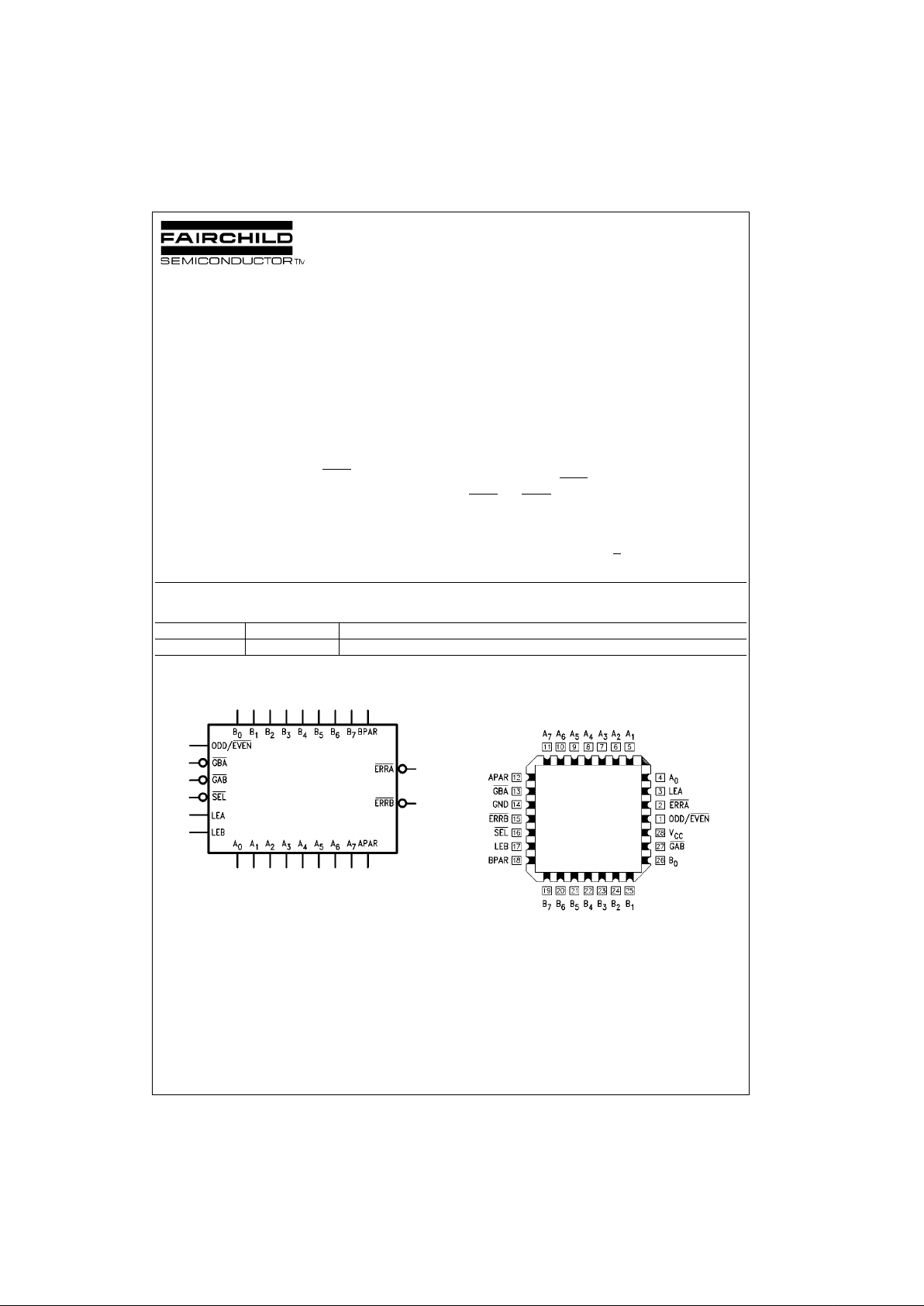
Logic Symbol Connection Diagram
Pin Assignment for PCC
FACT is a tra demark of Fairchild Semico nductor Corporation.
Order Number Package Number Package Description
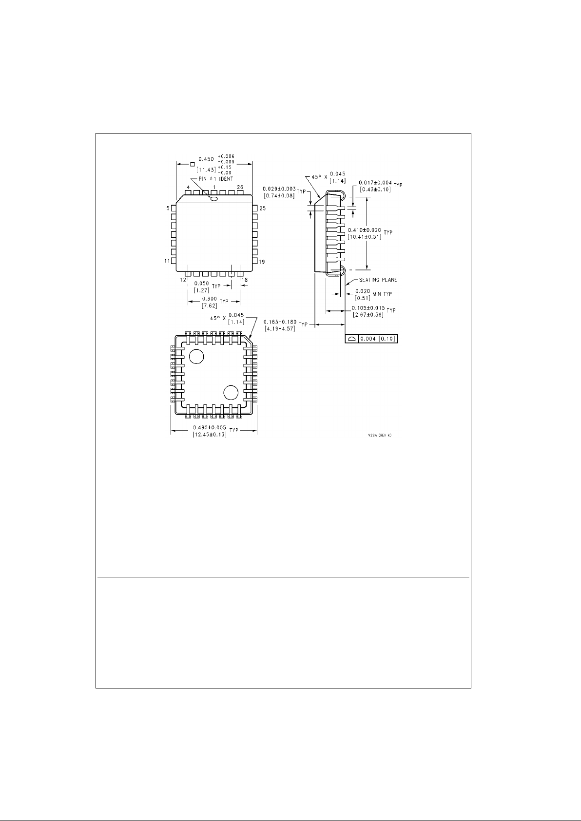
74ACT899QC V28A 28-Lead Plastic Lead Chip Carrier (PLCC), JEDEC MO-047, 0.450” Square
Page 2
www.fairchildsemi.com 2
74ACT899
Pin Descriptions Functional Description
The ACT899 has three prin cipal m odes o f opera tion which
are outlined below. These modes apply t o both the A- to-B
and B-to-A directions.
• Bus A (B) communicates to Bus B ( A), parity is generated and passed on to the B (A) Bus as BPAR (APAR). If
LEB (LEA) is HIGH and t he Mode Sele ct ( SEL
) is LOW,
the parity generated from B[0:7] (A[0:7]) can be checked
and monitored by ERRB
(ERRA).
• Bus A (B) communicates to Bus B (A) in a feed-through
mode if SEL
is HIGH. Parity is still generated and
checked as ERRA
and ERRB in the feed-th rough mo de
(can be used as an interru pt to signal a data/parity bit
error to the CPU).
• Independent Latch E nables (LEA and LEB) allow oth er
permutations of generating/checking (see Function
Table).
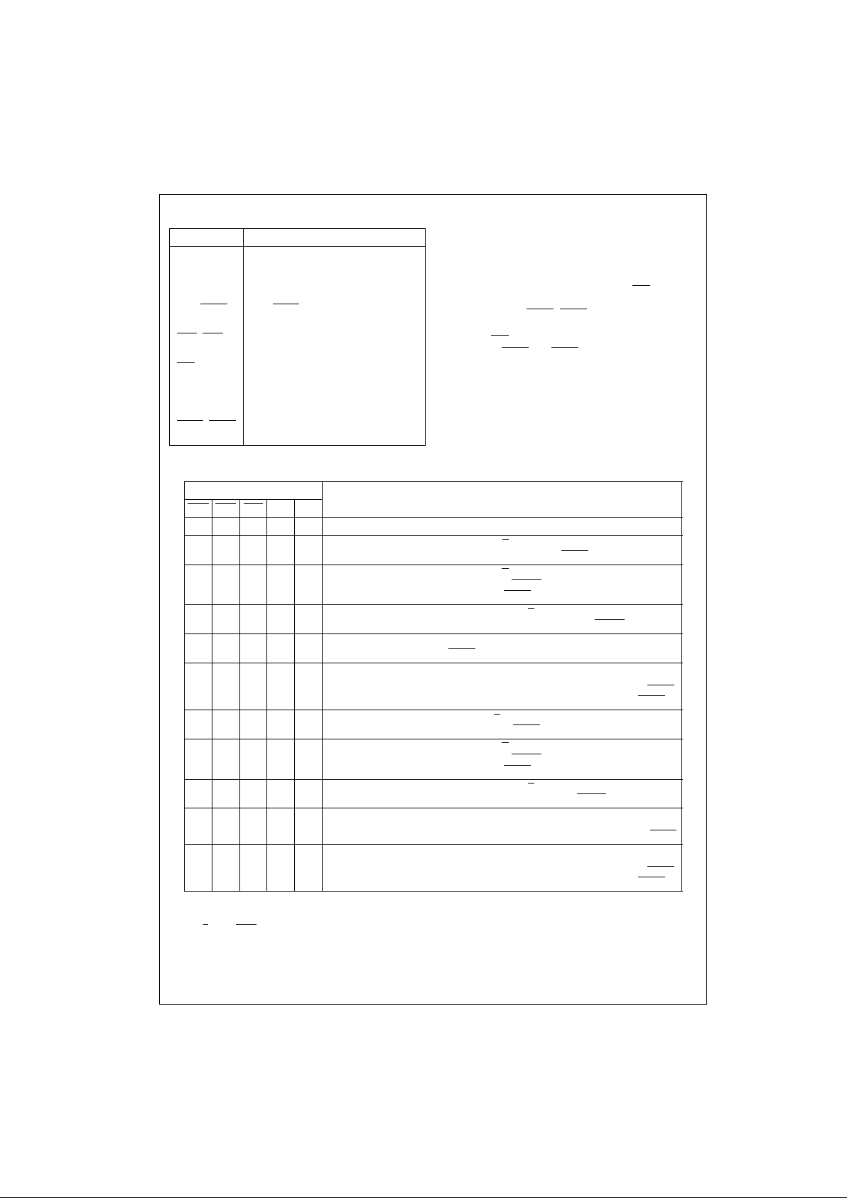
Function Table
H = HIGH Voltage Level
L = LOW V oltage Level
X = Immaterial
Note 1: O/E
= ODD/EVEN
Pin Names Description
A
0–A7
A Bus Data Inputs/Data Outputs
B
0–B7
B Bus Data Inputs/Data Outputs
APAR, BPAR A and B Bus Parity Inputs
ODD/EVEN
ODD/EVEN Parity Select,
Active LOW for EVEN Parity
GBA
, GAB Output Enables for A or B Bus,
Active LOW
SEL
Select Pin for Feed-Through or Generate
Mode, LOW for Generate Mode
LEA, LEB Latch Enables for A and B Latches,
HIGH for Transparent Mode
ERRA
, ERRB Error Signals for Checking Generated
Parity with Parity In, LOW if Error Occurs
Inputs Operation
GAB
GBA SEL LEA LEB
H H X X X Busses A and B are 3-STATE.
H L L L H Generates parity from B[0:7] based on O/E
(Note 1). Generated parity → APAR.
Generated parity checked against BPAR and output as ERRB
.
H L L H H Generates parity from B[0:7] based on O/E
. Generated parity → APAR. Generated
parity checked against BPAR and output as ERRB
. Generated parity also fed back
through the A latch for generate/check as ERRA
.
H L L X L Generates parity from B latch data based on O/E
. Generated parity → APAR.
Generated parity checked against latched BPAR and output as ERRB
.
HLHXHBPAR/B[0:7] → APAR/A0:7] Feed-through mode. Generated parity checked
against BPAR and output as ERRB
.
HLHHHBPAR/B[0:7] → APAR/A[0:7]
Feed-through mode. Generated parity checked against BPAR and output as ERRB
.
Generated parity also fed back through the A latch for generate/check as ERRA
.
L H L H L Generates parity for A[0:7] based on O/E
. Generated parity → BPAR. Generated
parity checked against APAR and output as ERRA
.
L H L H H Generates parity from A[0:7] based on O/E
. Generated parity → BPAR. Generated
parity checked against APAR and output as ERRA
. Generated parity also fed back
through the B latch for generate/check as ERRB
.
L H L L X Generates parity from A latch data based on O/E
. Generated parity → BPAR. Gen-
erated parity checked against latched APAR and output as ERRA
.
LHHHLAPAR/A[0:7] → BPAR/B[0:7]
Feed-through mode. Generated parity checked against APAR and output as ERRA
.
LHHHHAPAR/A[0:7] → BPAR/B[0:7]
Feed-through mode. Generated parity checked against APAR and output as ERRA
.
Generated parity also fed back through the B latch for generate/check as ERRB
.
Page 3
3 www.fairchildsemi.com
74ACT899
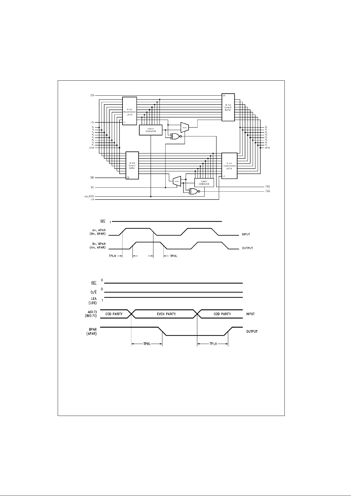
Functional Block Diagram
AC Path
An, APAR → Bn, BPAR
(B
n
, BPAR → An, APAR)
FIGURE 1.
An → BPAR
(B
n
→ APAR)
FIGURE 2.
Page 4
www.fairchildsemi.com 4
74ACT899
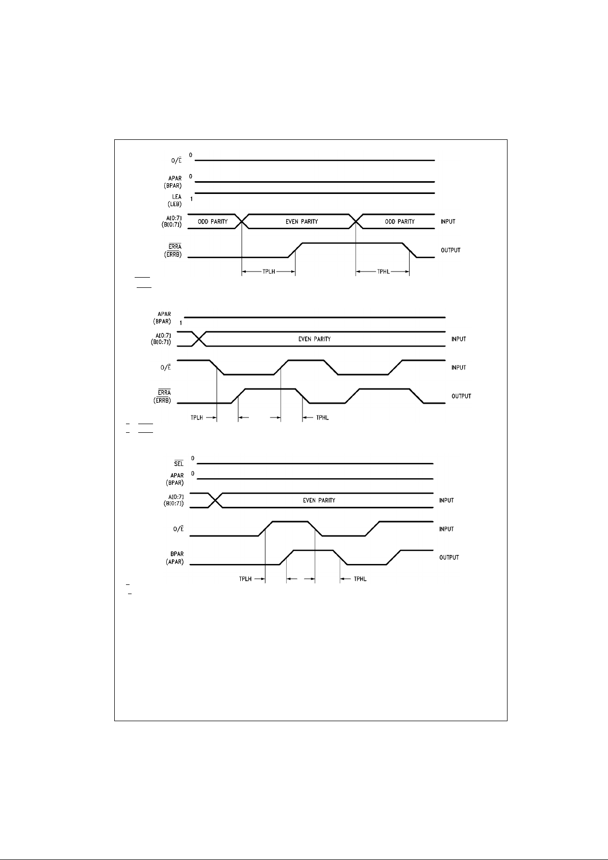
An → ERRA
(Bn → ERRB)
FIGURE 3.
O/E → ERRA
O/E → ERRB
FIGURE 4.
O/E → BPAR
(O/E
→ APAR)
FIGURE 5.
Page 5
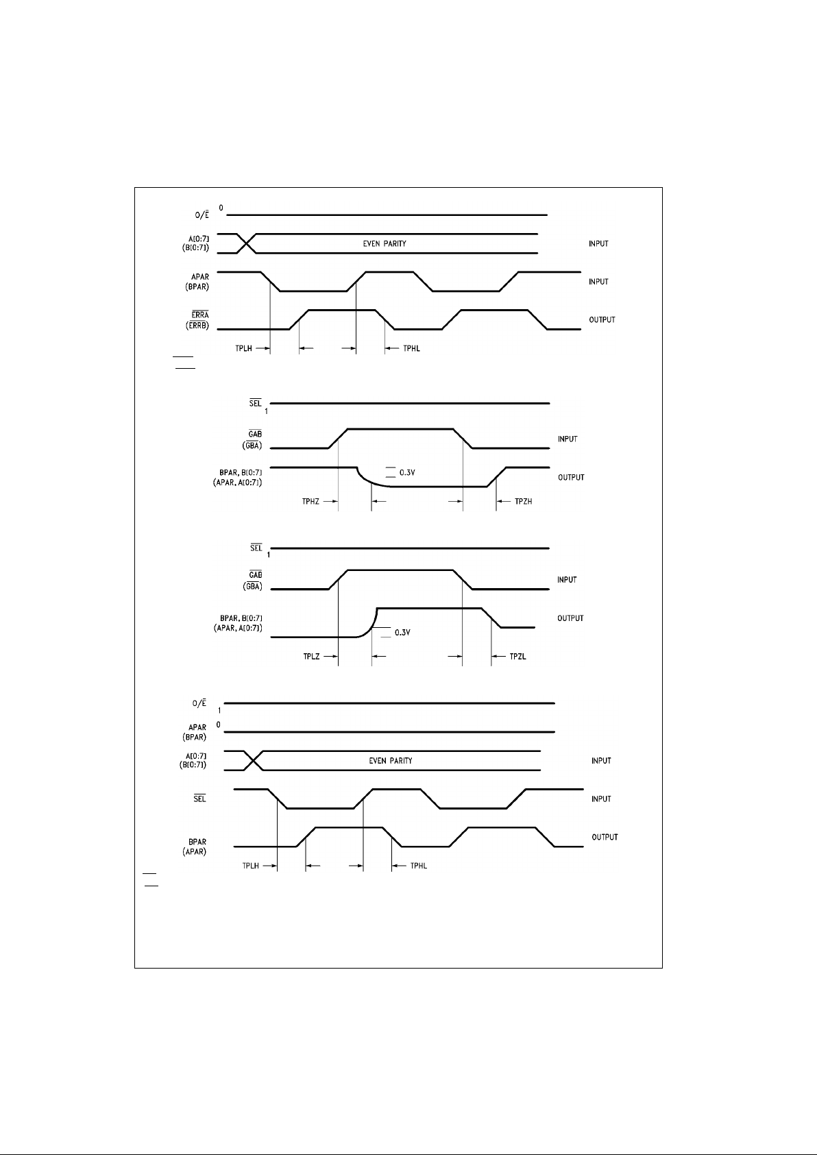
5 www.fairchildsemi.com
74ACT899
APAR → ERRA
(BPAR → ERRB)
FIGURE 6.
ZH, HZ
FIGURE 7.
ZL, LZ
FIGURE 8.
SEL → BPAR
(SEL
→ APAR)
FIGURE 9.
Page 6
www.fairchildsemi.com 6
74ACT899
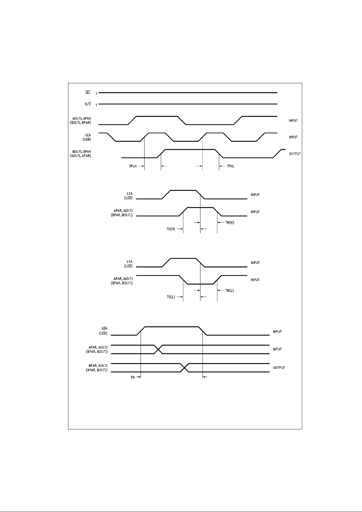
LEA → BPAR, B[0:7]
(LEB → APAR, A[0:7])
FIGURE 10.
TS(H), TH(H)
LEA → APAR, A[0:7]
(LEB → BPAR, B[0:7])
FIGURE 11.
TS(L), TH(L)
LEA → APAR, A[0:7]
(LEB → BPAR, B[0:7])
FIGURE 12.
FIGURE 13.
Page 7
7 www.fairchildsemi.com
74ACT899
Absolute Maximum Ratings(Note 2)
Recommended Operating
Conditions
Note 2: Absolute maximum ratings are those values beyond which damage
to the device may occur. The databook specifications should be met, without exception, to ensure that the system design is reliable over its power
supply, temperature, and output/in put loading variables. Fairchild does n ot
recommend operat ion of FACT circuits outside databook specifications.
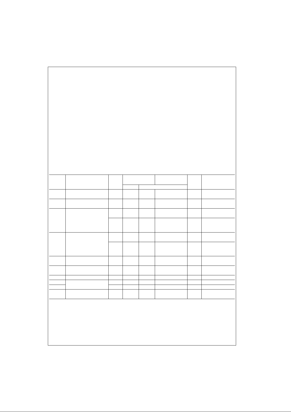
DC Electrical Characteristics
Note 3: Maximum of 9 outputs loaded; thresholds on input associated with output under test.
Note 4: Maximum test duration 2.0 ms, one output loaded at a time.
Supply Voltage (VCC) −0.5V to +7.0V
DC Input Diode Current (I
IK
)
V
I
= −0.5V −20 mA
V
I
= VCC + 0.5V +20 mA
DC Input Voltage (V
I
) −0.5V to VCC + 0.5V
DC Output Diode Current (I
OK
)
V
O
= −0.5V −20 mA
V
O
= VCC + 0.5V +20 mA
DC Output Voltage (V
O
) −0.5V to VCC + 0.5V
DC Output Source
or Sink Current (I
O
) ±50 mA
DC V
CC
or Ground Current
per Output Pin (I
CC
or I
GND
) ±50 mA
Storage Temperature (T
STG
) −65°C to +150°C
DC Latch-Up Source or
Sink Current ±300 mA
Junction Temperature (T
J
)140°C
Supply Voltage (V
CC
) 4.5V to 5.5V
Input Voltage (V
I
) 0V to V
CC
Output Voltage (VO) 0V to V
CC
Operating Temperature (TA) −40°C to +85°C
Minimum Input Edge Rate ∆V/∆t 125 mV/ns
V
IN
from 0.8V to 2.0V
V
CC
@ 4.5V, 5.5V
Symbol Parameter
V
CC
TA = +25°CTA = −40°C to +85°C
Units Conditions
(V) Typ Guaranteed Limits
V
IH
Minimum HIGH Level 4.5 1.5 2.0 2.0 V V
OUT
= 0.1V
Input Voltage 5.5 1.5 2.0 2.0 or VCC − 0.1V
V
IL
Maximum LOW Level 4.5 1.5 0 .8 0.8 V V
OUT
= 0.1V
Input Voltage 5.5 1.5 0.8 0.8 or VCC − 0.1V
V
OH
Minimum HIGH Level 4.5 4.49 4.4 4.4 V I
OUT
= −50 µA
Output Voltage 5.5 5.49 5.4 5.4
VIN = V
IL
or V
IH
4.5 3.86 3.76 V IOH = −24 mA
5.5 4.86 4.76 IOH = −24 mA (Note 3)
V
OL
Maximum LOW Level 4.5 0.001 0.1 0.1 V I
OUT
= 50 µA
Output Voltage 5.5 0.001 0.1 0.1
VIN = VIL or V
IH
4.5 0.36 0.44 V IOL = 24 mA
5.5 0.36 0.44 IOL = 24 mA (Note 3)
I
IN
Maximum Input 5.5 ±0.1 ±1.0 µAVI = VCC, GND
Leakage Current
I
OZ
Maximum 3-STATE 5.5 ±0.5 ±5.0 µAVI = VIL, V
IH
Leakage Current VO = VCC, GND
I
CCT
Maximum ICC/Input 5.5 0.6 1.5 mA VI = VCC − 2.1V
I
OLD
Minimum Dynamic 5.5 75 mA V
OLD
= 1.65V Max
I
OHD
Output Current (Note 4) 5.5 −75 mA V
OHD
= 3.85V Min
I
CC
Maximum Quiescent 5.5 8.0 80.0 µAVIN = V
CC
Supply Current or GND
Page 8
www.fairchildsemi.com 8
74ACT899
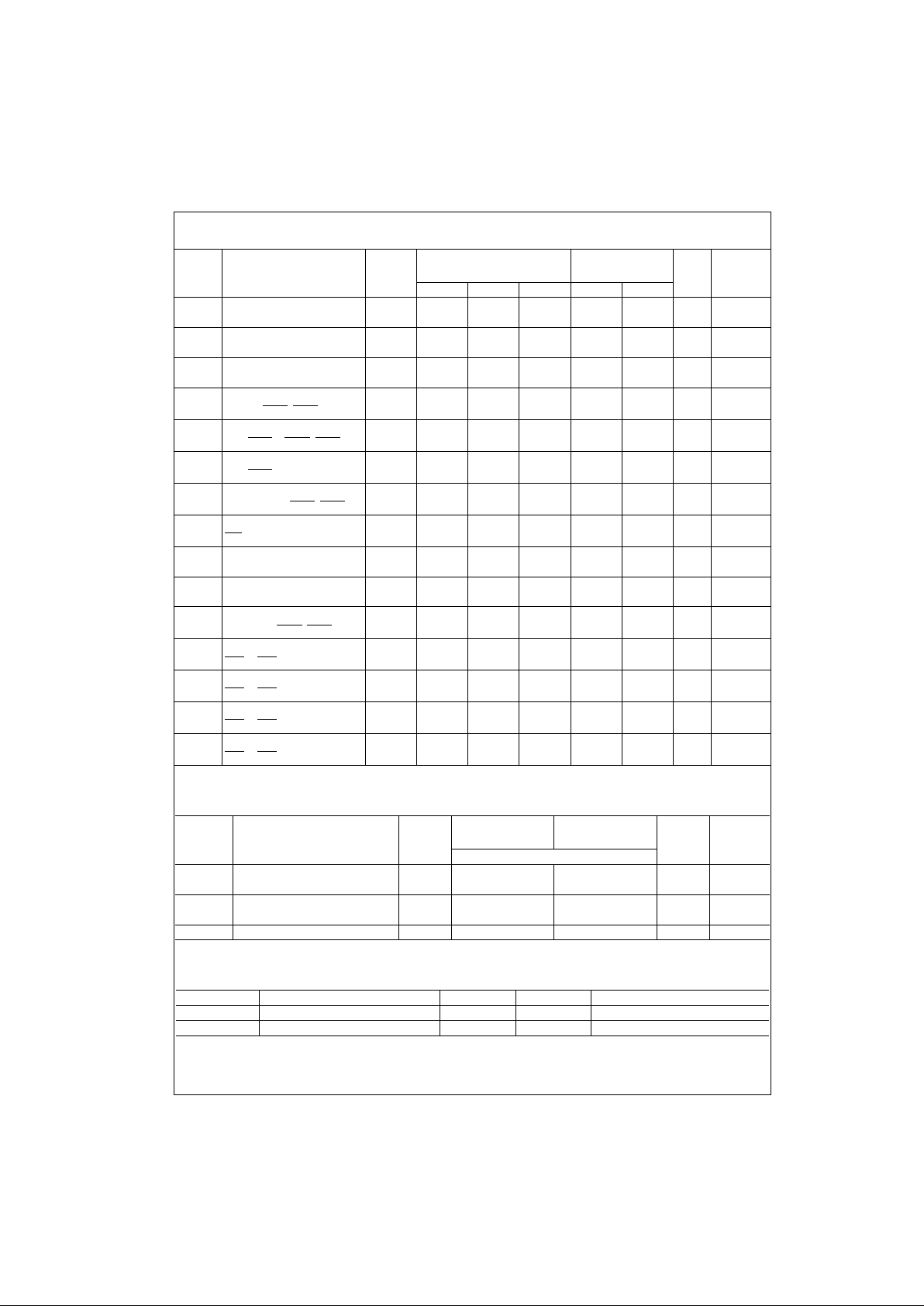
AC Electrical Charac teristics
Note 5: Voltage Range 5.0 is 5.0V ± 0.5V.
AC Operating Requirements
Note 6: Voltage Range 5.0 = 5.0V ± 0.5V.
Capacitance
V
CC
TA = +25°CT
A
= −40°C to +85°C
Symbol Parameter (V)
CL = 50 pF CL = 50 pF
Units Fig. No.
(Note 5) Min Typ Max Min Max
t
PLH
Propagation Delay 5.0 2.5 7.5 11.5 2.5 12.0 ns Figure 1
t
PHL
An, Bn to Bn, A
n
t
PLH
Propagation Delay 5.0 1.5 6.0 8.5 1.5 9.0 ns Figure 1
t
PHL
APAR, BPAR to BPAR, APAR
t
PLH
Propagation Delay 5.0 2.5 8.5 12.0 2.5 12.5 ns Figure 2
t
PHL
An, Bn to BPAR, APAR
t
PLH
Propagation Delay 5.0 2.0 8.0 11.5 2.0 12.0 ns Figure 3
t
PHL
An, Bn to ERRA, ERRB
t
PLH
Propagation Delay 5.0 2.0 8.0 11.5 2.0 12.0 ns Figure 4
t
PHL
ODD/EVEN to ERRA, ERRB
t
PLH
Propagation Delay 5.0 2.5 8.0 11.5 2.5 12.0 ns Figure 5
t
PHL
ODD/EVEN to APAR, BPAR
t
PLH
Propagation Delay 5.0 1.5 7.5 10.5 1.5 11.5 ns Figure 6
t
PHL
APAR, BPAR to ERRA, ERRB
t
PLH
Propagation Delay 5.0 1.5 6.5 9.0 1.5 9.5 ns Figure 9
t
PHL
SEL to APAR, BPAR
t
PLH
Propagation Delay 5.0 2.5 7.0 10.5 2.5 11.0 ns Figure 10
t
PHL
LEB to An, B
n
Figure 11
t
PLH
Propagation Delay 5.0 2.0 8.0 11.5 2.0 12.0 ns Figure 10
t
PHL
LEA to APAR, BPAR Figure 11
t
PLH
Propagation Delay 5.0 2.5 8.0 11.5 2.5 12.0 ns Figure 12
t
PHL
LEA, LEB to ERRA, ERRB
t
PZH
Output Enable Time 5.0 2.5 7.0 10.5 2.5 11.0 ns Figure 7
t
PZL
GBA or GAB to An, B
n
Figure 8
t
PZH
Output Enable Time 5.0 1.5 6.0 9.0 1.5 9.5 ns Figure 7
t
PZL
GBA or GAB to BPAR or APAR
Figure 8
t
PHZ
Output Disable Time 5.0 1.5 6.5 9.5 1.5 9.5 ns Figure 7
t
PHL
GBA or GAB to An, B
n
Figure 8
t
PHZ
Output Disable Time 5.0 1.5 6.5 9.5 1.5 9.5 ns Figure 7
t
PLZ
GBA or GAB to BPAR, APAR
Figure 8
V
CC
TA = +25°C TA = −40°C to +85°C
Symbol Parameter (V)
CL = 50 pF CL = 50 pF
Units Fig. No.
(Note 6) Guaranteed Minimum
t
S
Setup Time, HIGH or LOW 5.0 3.0 3.0 ns Figure 11
An, Bn, PAR to LEA, LEB Figure 12
t
H
Hold Time, HIGH or LOW 5.0 1.5 1.5 ns Figure 11
An, Bn, PAR to LEA, LEB Figure 12
t
W
Pulse Width for LEB, LEA 5.0 4.0 4.0 ns Figure 13
Symbol Parameter Typ Units Conditions
C
IN
Input Capacitance 4.5 pF VCC = 5.0V
C
PD
Power Dissipation Capacitance 210 pF VCC = 5.0V
Page 9
Fairchild does not assume any responsibility for use of any circuitry described, no circuit patent licenses are implied and Fairchild reser ves the right at any time without notice to change said circuitry and specifications.
74ACT899 9-Bit Latchable Transceiver with Parity Generator/Checker
LIFE SUPPORT POLICY
FAIRCHILD’S PRODUCTS ARE NOT AUTHORIZED FOR USE AS CRITICAL COMPONENTS IN LIFE SUPPORT
DEVICES OR SYSTEMS WITHOUT THE EXPRESS WRITTEN APPROVAL OF THE PRESIDENT OF FAIRCHILD
SEMICONDUCTOR CORPORATION. As used herein:
1. Life support devices or systems are devices or syste ms
which, (a) are intended for surgical implant into the
body, or (b) support or sustain life, and (c) whose failure
to perform when properly used in accordance with
instructions for use provided in the labeli n g, can be re asonably expected to result i n a significant injur y to the
user.
2. A critical com ponen t in any com ponen t of a li fe support
device or system whose failure to perform can be reasonably expected to cause the failure of the life support
device or system, or to affect its safety or effectiveness.
www.fairchildsemi.com
Physical Dimensions inches (millimeters) unless otherwise noted
28-Lead Plastic Lead Chip Carrier (PLCC), JEDEC MO-047, 0.450” Square
Package Number V28A
 Loading...