

Page 1
■ OPERATES4 LATCHINGRELAIS, 1SINGLE
SIDESTABLERELAYAND1 LED
■ VERYLOWPOWERCONSUMPTION
■
TTL COMPATIBLEINPUT THRESHOLDS
■ IMPROVEDLATCH-UP IMMUNITY UPTO
300mA
■
TSSOP-20PACK AGE
DESCRIPTION
The device is a relais driver for line card
application. It is able to operate four latching
relais, one single side stable relay and one LED
connected either to GND or VCC. All the outputs
can be set to LOW with the RST input as shown
in thetrue table.
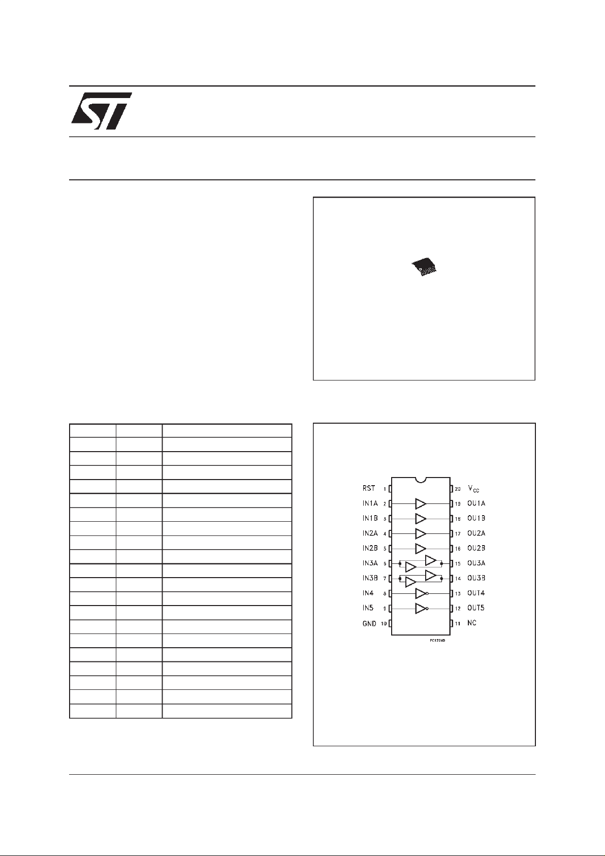
74ACT8244
RELAY DRIVER IC
T
(TSSOPPackage)
ORDERCODES :
74ACT8244TTR
PIN DESCRIPTION
PI N No SYMB O L NAM E AND F UNCT ION
1 RST Master Reset
2 IN1A Input of 1st latched relay drv
3 IN1B Input of 1st latched relay drv
4 IN2A Input of 2nd latched relay drv
5 IN2B Input of 2nd latched relay drv
6 IN3A Input of 3rd latched relay drv
7 IN3B Input of 3rd latched relay drv
8 IN4 Input of 1st relay driver
9 IN5 Input LED driver
10 GND Ground
11 NC Not Connected
12 OUT5 Output of LED driver
13 OUT4 Output of 1st relay driver
14 OU3B Output 3rd latched relay drv
15 OU3A Output 3rd latched relay drv
16 OU2B Output 2nd latched relay drv
17 OU2A Output 2nd latched relay drv
18 OU1B Output 1st latched relay drv
19 OU1A Output 1st latched relay drv
20 V
CC
Supply Voltage
LOGICDIAGRAM
November 1999
1/6
Page 2

74ACT8244
ABSOLUTE MAXIMUMRATINGS
Symb o l Para met er Val u e Uni t
V
V
V
I
I
OK
I
orI
I
CC
T
AbsoluteMaximumRatingsarethosevaluesbeyond whichdamagetothedevicemayoccur. Functionaloperationunderthesecondition isnotimplied.
RECOMMENDEDOPERATINGCONDITIONS
Symb o l Parameter Val u e Uni t
V
V
V
T
dt/dv Input Rise and Fall Time V
1)VINfrom0.8V to2.0V
Supply Voltage -0.5to+7 V
CC
DC Input Voltage -0.5toVCC+0.5 V
I
DC Output Voltage -0.5toVCC+0.5 V
O
DC Input Diode Current ±50 mA
IK
DC Output Diode Current ±50 mA
DC Output Current
O
DC VCCor Ground Current
GND
Storage Temperature -65to+150
stg
Supply Voltage 4.75to5.25 V
CC
Input Voltage 0toV
I
Output Voltage 0toV
O
Operating Temperature: -30to+80
op
= 4.5 to 5.5V (note1) 10 ns/V
CC
100 mA
±
400 mA
±
CC
CC
o
C
V
V
o
C
DC SPECIFICATIONS (Electricalcharacteristics over recommendedoperating conditions)
Symb o l Parame t er Test Cond ition s Value Unit
Min. T yp. Max.
High Level Input Threshold VO=0.1V or VCC- 0.1 V 2.0 1.4 V
V
IH
Low Level Input Threshold VO=0.1V or VCC- 0.1 V 1.4 0.8
V
IL
High Level Output Voltage for
V
OH
Single Driver
Low Level Output Voltage for
V
OL
Single Driver
High Level Output Voltage for
V
OH
Double Relay Driver
Low Level Output Voltage for
V
OL
Double Relay Driver
High Level Output Voltage for
V
OH
Single Side Relay or LED
Low Level Output Voltage for
V
OL
Single Side Relay or LED
Input Leakage Current VI=VCCor GND ±1 µA
I
I
Max ICC/Input VI=VCC-2.1V 0.6 1.5 mA
I
CCT
Quiescent Supply Current VI=VCCor GND 4 40 µA
I
CC
I
=-35mA VCC-0.68 VCC-0.3 V
OUT
I
= 35mA 0.25 0.68 V
OUT
I
=-70mA VCC-0.68 VCC-0.3 V
OUT
I
= 70mA 0.25 0.68 V
OUT
I
=-50mA VCC-0.8 VCC-0.4 V
OUT
I
=50mA 0.3 0.8 V
OUT
V
2/6
Page 3

74ACT8244
AC ELECTRICAL CHARACTERISTICS
Symbol Parameter Test Condition Value Unit
t
Propagation Delay Time Overrecommendedoperating
PLH
t
PHL
TRUTH TABLE FOR LATCHINGRELAY
DRIVER
INPUT OUTPUT Condition
RST INn A INn B O U n A OUnB
HXXLLStorage
LLLLLStorage
LLHLHOperate
L H L H L Release
LHHHHStorage
Z = High Impedance
X=Don’tCare
n=1,2,3
= 50 pF, RL= 500 Ω, Inputtr=tf=3 ns)
(C
L
Min. T yp. Max.
conditions
TRUTH TABLE FORSINGLE SIDE RELAY
INPUT OUTPU T
IN4 OUT4
LH
HL
TRUTH TABLE FORLED DRIVER
INPUT OUTPU T
IN5 OUT5
LH
HL
7.0 11.0 ns
OUTPUT CIRCUIT FOR LATCHING RELAYDRIVER
OUTPUT CIRCUIT FOR SINGLESIDE RELAY OUTPUT CIRCUIT FOR LED DRIVER
3/6
Page 4

74ACT8244
OutputCharacteristics of a DoubleRelay Driver
N-channelwith All OutputsLoaded
OutputCharacteristics of a SingleSide Relay or
Led Driver N-channelwith All OutputsLoaded
OutputCharacteristics of a DoubleRelay Driver
P-channelwith All OutputsLoaded
OutputCharacteristics of a Single Side Relayor
Led Driver P-channelwith All OutputsLoaded
4/6
Page 5
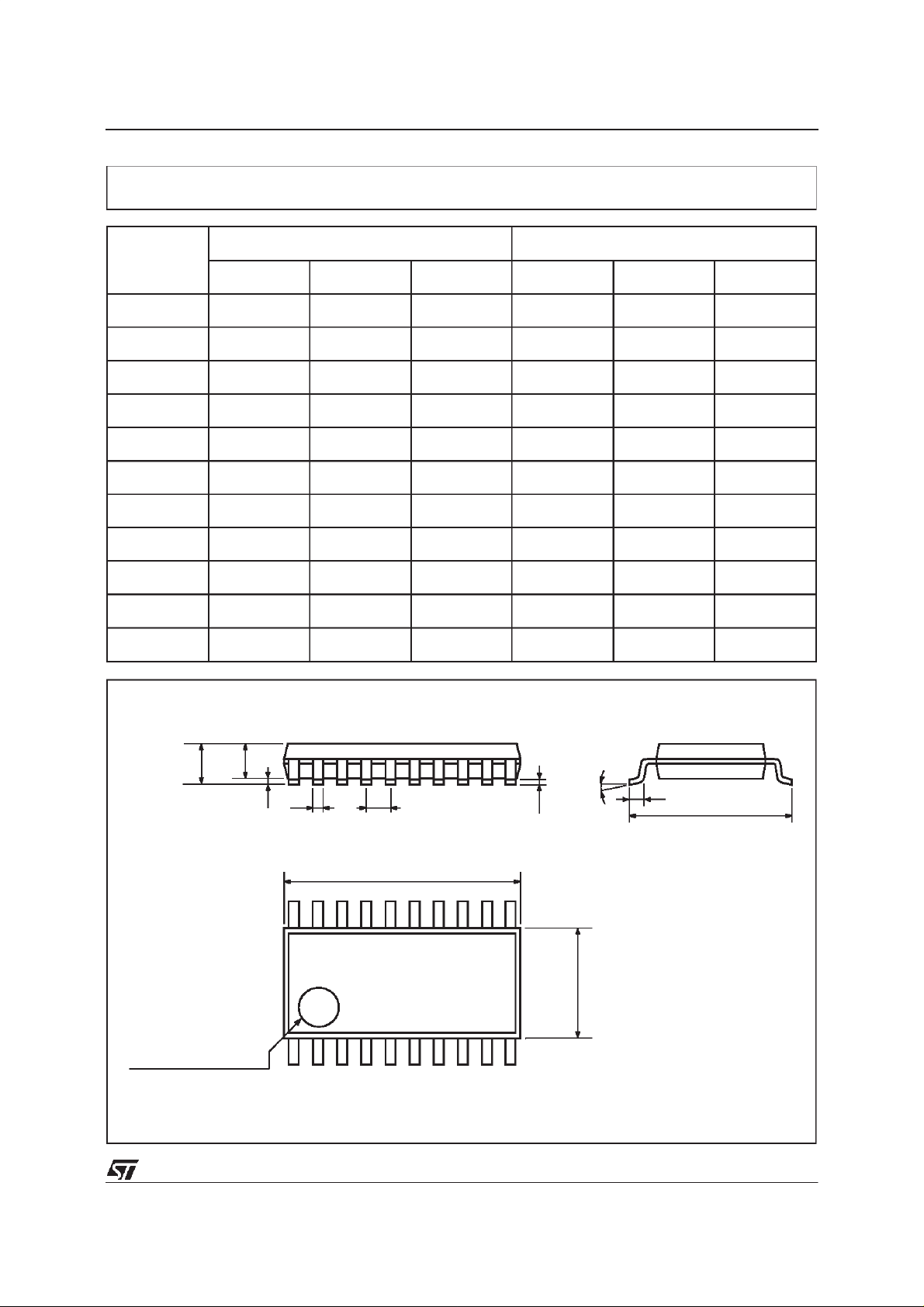
TSSOP20 MECHANICAL DATA
74ACT8244
DIM.
mm inch
MIN. TYP. MAX. MIN. TYP. MAX.
A 1.1 0.433
A1 0.05 0.10 0.15 0.002 0.004 0.006
A2 0.85 0.9 0.95 0.335 0.354 0.374
b 0.19 0.30 0.0075 0.0118
c 0.09 0.2 0.0035 0.0079
D 6.4 6.5 6.6 0.252 0.256 0.260
E 6.25 6.4 6.5 0.246 0.252 0.256
E1 4.3 4.4 4.48 0.169 0.173 0.176
e 0.65 BSC 0.0256 BSC
K0
o
o
4
o
8
o
0
o
4
L 0.50 0.60 0.70 0.020 0.024 0.028
o
8
A2
A
A1
PIN 1 IDENTIFICATION
b
e
K
c
L
E
D
E1
1
5/6
Page 6

74ACT8244
Information furnished is believed to be accurate and reliable.However, STMicroelectronics assumes no responsibility for the consequences
of use of such information nor for any infringement of patents or other rights of third parties which may result from its use. No license is
granted by implicationor otherwise under any patent or patent rightsof STMicroelectronics. Specification mentioned in this publication are
subject to change without notice. This publicationsupersedes andreplacesallinformation previously supplied. STMicroelectronics products
are not authorized for use ascritical components in life support devices or systems withoutexpress written approval of STMicroelectronics.
The ST logois a registered trademark of STMicroelectronics
1999 STMicroelectronics – Printedin Italy– AllRights Reserved
STMicroelectronics GROUP OF COMPANIES
Australia - Brazil -China - Finland- France- Germany - Hong Kong - India - Italy - Japan-Malaysia - Malta - Morocco
Singapore - Spain - Sweden - Switzerland - United Kingdom- U.S.A.
http://www.st.com
.
6/6
 Loading...