

Page 1
© 2000 Fairchild Semiconductor Corporation DS009801 www.fairchildsemi.com
July 1988
Revised September 2000
74ACT818 8-Bit Diagnostic Register
74ACT818
8-Bit Diagnostic Register
General Description
The ACT818 is a high-speed, general-purpose pipeline
register with an on-bo ar d dia gno sti c re giste r fo r performing
serial diagnostics and/or writable control store loading.
The D-to-Y path pr ovides an 8-b it parallel data path pipeline register for normal system operation. The diagnostic
register can load parallel data to or fro m the pipel ine register and can output data through the D input por t (as in
WCS loading).
The 8-bit diagnostic register has multiplexer inputs that
select parallel inp uts from the Y-port or adjacent bi ts i n the
diagnostic register to operate as a right -shift-only regist er.
This register can then participate in a serial loop throughout
the system where normal da ta, a ddr ess, statu s and cont rol
registers are replaced with ACT818 diagnostic pipeline registers. The loop can be used to scan in a complete test routine starting point (Data, Address, etc.). Then after a
specified number of machine cycles it scans out the results
to be inspected for the expect ed resu lts. WC S load ing c an
be accomplished usin g the same t echniqu e. An i nstruct ion
word can be serially shifted into the shadow register and
written into the WCS RAM by enabling the D output.
Features
■ On-line and off-line system diagnostics
■ Swaps the contents of diagnostic register and output
register
■ Diagnostic register and diagnostic testing
■ Cascadable for wide control word s as use d in mi crop ro-
gramming
■ Edge-triggered D registers
■ Outputs source/sink 24 mA
■ ACT818 has TTL-compatible inputs
■ ACT818 is functionally- and pin-compatible to AMD
Am29818 and MMI 74S818
Applications
• Register for microprogram control store
• Status register
• Data register
• Instruction register
• Interrupt mask register
• Pipeline register
• General purpose register
• Parallel-serial/serial-parallel converter
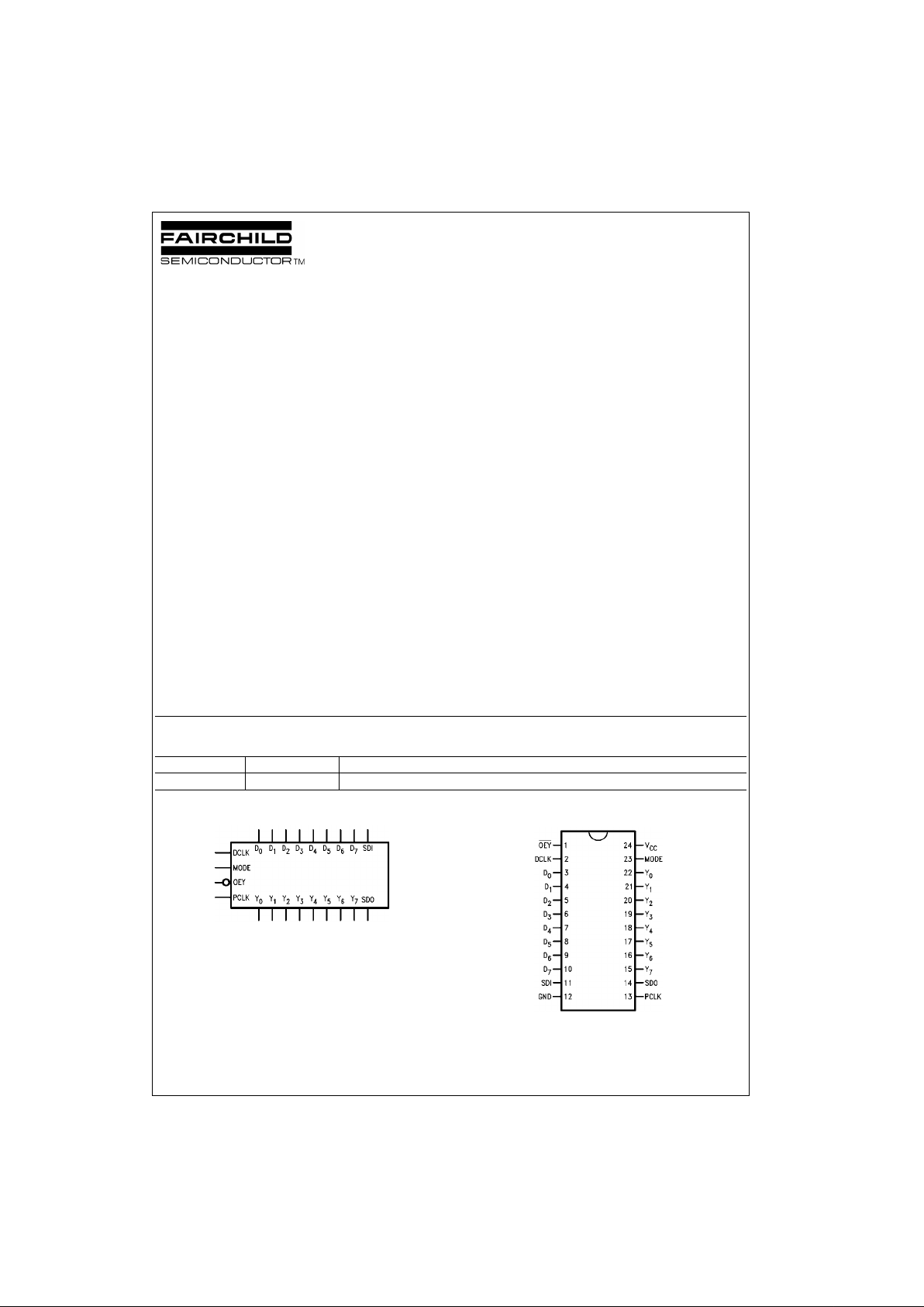
Ordering Code:
Logic Symbol Connection Diagram
FACT is a trademark of Fairchild Semiconductor Corporation.
Order Number Order Package Package Description
74ACT818SPC N24C 24-Lead Plastic Dual-In-Line Package (PDIP), JEDEC MS-001, 0.300 Wide
Page 2
www.fairchildsemi.com 2
74ACT818
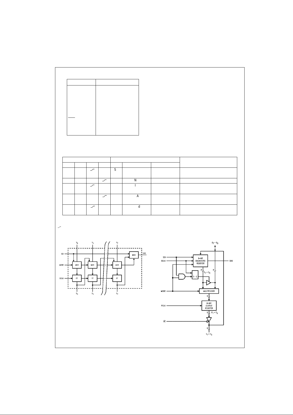
Pin Descriptions Functional Description
Data transfers into the diagnostic register occur on the
LOW-to-HIGH transition of DCLK. Mode and SDI determine what data source will be loaded. The pipeline register
is loaded on the LOW-to-HIGH tr ansition of PCLK. Mode
selects whether the d ata source is the data input or the
diagnostic register output. Because of the independence of
the clock inputs, data can be shifted in the diagnostic register via DCLK and loaded i nto t he pipel ine re giste r from the
data input via PCLK simultaneously, as long as no setup or
hold times are violated. This simultaneous operation is
legal.
Function Table
H = HIGH Voltage Level
L = LOW Voltage Level
X = Immaterial
= LOW-to-HIGH Clo c k Transi ti on
Diagnostic Register Block Diagram
Pin Names Description
D
0–D7
Data Inputs
SDI Serial Data Input
DCLK Diagnostics Clock
MODE Control Input
PCLK Pipeline Register Clock
OEY
Output Enable Input
SDO Serial Data Output
Y
0–Y7
Data Outputs
Inputs Outputs
Operation
SDI MODE DCLK PCLK SDO Diagnostic Reg. Pipeline Reg.
XL
XS7 SI<SI − 1, NA Serial Shift; D7–D0 Disabled
SO
<SD
I
XLX
S7 NA PI<DI Normal Load Pipeline Register
LH
XL SI<YI NA Load Diagnostic Register from Y;
DI Disabled
XHX
SDI NA PI<SI Load Pipeline Register from
Diagnostic Register
HH
X H Hold NA Hold Diagnostic Register; DI
Enabled
Page 3

3 www.fairchildsemi.com
74ACT818
Absolute Maximum Ratings(Note 1) Recommended Operating
Conditions
Note 1: Absolute max imum rating s are those va lues beyon d which damag e
to the device may occu r. The databook spe cificatio ns shou ld be met, wit hout exception, to ensure that the system de sign is relia ble over its p ower
supply, temperature, and output/input loading variables. Fairchild does not
recommend operation of FACT circuits outside databook specificat ions.
DC Electrical Characteristics
Note 2: All outputs loaded; thres holds on input associate d w it h output under test.
Note 3: Test load 50 pF, 500Ω to ground.
Supply Voltage (VCC) −0.5V to +7.0V
DC Input Diode Current (I
IK
)
V
I
= −0.5V −20 mA
V
I
= VCC +0.5V +20 mA
DC Input Voltage (V
I
) −0.5V to VCC +0.5V
DC Output Diode Current (I
OK
)
V
O
= −0.5V −20 mA
V
O
= VCC + 0.5V +20 mA
DC Output Voltage (V
O
) −0.5V to VCC + 0.5V
DC Output S ource
or Sink Current (I
O
) ± 50 mA
DC V
CC
or Ground Current
per Output Pin (I
CC
or I
GND
) ± 50 mA
Storage Temperature (T
STG
) −65°C to +150°C
Junction Temperature (T
J
)
PDIP 140
°C
Supply Voltage (V
CC
) 4.5V to 5.5V
Input Voltage (V
I
)0V to V
CC
Output Voltage (VO)0V to V
CC
Operating Temperature (TA) −40°C to +85°C
Minimum Input Edge Rate (
∆V/∆t) 125 mV/ns
V
IN
from 0.8V to 2.0V
V
CC
@ 4.5V, 5.5V
Symbol Parameter
V
CC
TA = +25°CT
A
= −40°C to +85°C
Units Conditions
(V) Typ Guaranteed Limits
V
IH
Minimum HIGH Level 4.5 1.5 2.0 2.0
V
V
OUT
= 0.1V
Input Voltage 5.5 1.5 2.0 2.0 or VCC − 0.1V
V
IL
Maximum LOW Level 4.5 1.5 0.8 0.8
V
V
OUT
= 0.1V
Input Voltage 5.5 1.5 0.8 0.8 or V
CC
− 0.1V
I
IN
Maximum Input Leakage Current 5.5 ± 0.1 ± 1.0 µAVIN = V
CC
I
OZ
Maximum 3- STATE
5.5 ± 0.5 ± 5.0 µA
OE = V
IH
Leakage Current V
OUT
= 0V, V
CC
I
CC
Maximum Quiescent Supply Current 5.5 8.0 80.0 µAVIN = VCC or GND
I
CCT
Maximum Additional
5.5 1.5 mA
VIN = VCC − 2.1V
I
CC
/Input VCC = 5.5V
V
OH
Minimum HIGH VIN = V
IL
or V
IH
Level Output Voltage, 4.5 3.86 3.76 V IOH = −24 mA
Y
0–Y7
Outputs 5.5 4.86 4.76 V IOH =−24 mA (Note 2)
Minimum HIGH
Level Output Voltage, 4.5 3.86 3.76 V I
OH
= −8 mA
D0–D7, SDO Outputs 5.5 4.86 4.76 V IOH = −8 mA
V
OL
Maximum LOW VIN = VIL or V
IH
Level Output Voltage, 4.5 0.36 0.44 V IOL = 24 mA
Y0–Y7 Outputs 5.5 0.36 0.44 V IOL = 24 mA (Note 2)
Maximum LOW Level Output Voltage, 4.5 0.36 0.44 V IOL = 8 mA
D0–D7, SDO Outputs 5.5 0.36 0.44 V IOL = 8 mA
I
OLD
Minimum Dynamic Output Current
5.5 75 mA V
OLD
= 1.65V Max
Y0–Y7 Outputs
I
OHD
Minimum Dynamic Output Current
5.5
−75
mA V
OHD
= 3.85V Min
Y0–Y7 Outputs
I
OLD
Minimum Dynamic Output Current
5.5 32 mA V
OLD
= 1.65V Max
D0–D7, SDO Outputs (Note 3)
I
OHD
Minimum Dynamic Output Current
5.5 −32 mA V
OHD
= 3.85V Min
D0–D7, SDO Outputs (Note 3)
Page 4

www.fairchildsemi.com 4
74ACT818
AC Electrical Characteristics
Note 4: Voltage Range 5.0 is 5.0V ± 0.5V.
V
CC
TA = +25°CT
A
= −40°C to +85°C
Symbol Parameter (V)
C
L
= 50 pF CL = 50 pF
Units
(Note 4) Min Typ Max Min Max
t
PHL
Propagation Delay
5.0 3.0 6.0 9.0 2.5 9.5 ns
PCLK to Y
t
PLH
Propagation Delay
5.0 3.0 6.5 9.0 2.5 10.0 ns
PCLK to Y
t
PHL
Propagation Delay
5.0 4.0 8.0 11.0 3.5 12.0 ns
MODE to SDO
t
PLH
Propagation Delay
5.0 4.0 8.0 11.5 4.0 12.5 ns
MODE to SDO
t
PHL
Propagation Delay
5.0 3.5 7.5 10.5 3.0 12.0 ns
SDI to SDO
t
PLH
Propagation Delay
5.0 3.5 7.5 10.5 3.5 12.0 ns
SDI to SDO
t
PHL
Propagation Delay
5.0 4.5 9.0 12.5 4.0 14.0 ns
DCLK to SDO
t
PLH
Propagation Delay
5.0 4.5 9.5 13.0 4.0 14.5 ns
DCLK to SDO
t
PZL
Output Enable Time
5.0 2.5 6.0 9.0 2.5 10.0 ns
OEY to Y
n
t
PLZ
Output Disable Time
5.0 1.5 5.5 8.0 1.0 9.0 ns
OEY
to Y
n
t
PZL
Output Enable Time
5.0 3.0 8.0 12.0 3.0 13.5 ns
DCLK to D
n
t
PLZ
Output Disable Time
5.0 2.0 8.5 11.0 1.5 12.0 ns
DCLK to D
n
t
PZH
Output Enable Time
5.0 3.0 8.0 10.0 2.5 11.0 ns
OEY to Y
n
t
PHZ
Output Disable Time
5.0 2.5 9.0 11.0 2.0 11.5 ns
OEY
to Y
n
t
PZH
Output Enable Time
5.0 3.0 6.5 11.5 3.0 13.0 ns
DCLK to D
n
t
PHZ
Output Disable Time
5.0 3.0 7.5 12.0 2.0 13.0 ns
DCLK to D
n
Page 5

5 www.fairchildsemi.com
74ACT818
AC Operating Requirements
Note 5: Voltage range 5.0 is 5.0V ± 0.5V.
Capacitance
V
CC
TA = +25°CT
A
= −40°C to +85°C
Symbol Parameter (V)
C
L
= 50 pF CL = 50 pF
Units
(Note 5) Typ Guaranteed Minimum
t
S
Setup Time
5.0 1.0 4.0 5.0 ns
D to PCLK
t
H
Hold Time
5.0 0.0 1.0 1.0 ns
D to PCLK
t
H
Setup Time
5.0 2.5 4.5 5.5 ns
MODE to PCLK
t
H
Hold Time
5.0 −1.0 0.0 0.0 ns
MODE to PCLK
t
S
Setup Time
5.0 0.5 2.5 2.5 ns
Y to DCLK
t
S
Hold Time
5.0 0 1.0 1.5 ns
Y to DCLK
t
S
Setup Time
5.0 2.0 4.0 4.0 ns
MODE to DCLK
t
H
Hold Time
5.0 −0.5 1.0 1.0 ns
MODE to DCLK
t
S
Setup Time
5.0 2.0 3.5 4.5 ns
SDI to DCLK
t
H
Hold Time
5.0 −0.5 1.0 1.0 ns
SDI to DCLK
t
S
Setup Time
5.0 6.0 9.0 10.5 ns
DCLK to PCLK
t
S
Setup Time
5.0 6.0 11.0 11.5 ns
PCLK to DCLK
t
W
Pulse Width
5.0 2.0 3.0 3.0 ns
PCLK HIGH or LOW
t
W
Pulse Width
5.0 2.0 3.0 3.0 ns
DCLK HIGH or LOW
Symbol Parameter Typ Units Conditions
C
IN
Input Capacitance 4.5 pF VCC = OPEN
C
PD
Power Dissipation Capacitance 20 pF VCC = 5.0V
Page 6

www.fairchildsemi.com 6
74ACT818 8-Bit Diagnostic Register
Physical Dimensions inches (millimeters) unless otherwise noted
24-Lead Plastic Dual-In-Line Package (PDIP), JEDEC MS-001, 0.300 Wide
Package Number N24C
Fairchild does not assume any responsibility for use of any circuitr y described, no circuit patent licenses are implied and
Fairchild reserves the right at any time without notice to change said circuitry and specifications.
LIFE SUPPORT POLICY
FAIRCHILD’S PRODUCTS ARE NOT AUTHORIZED FOR USE AS CRITICAL COMPONENTS IN LIFE SUPPORT
DEVICES OR SYSTEMS WITHOUT THE EXPRESS WRITTEN APPROVAL OF THE PRESIDENT OF FAIRCHILD
SEMICONDUCTOR CORPORATION. As used herein:
1. Life support devices or systems are devices or syste ms
which, (a) are intended for surgical implant into the
body, or (b) support or sustain life, and (c) whose failure
to perform when properly used in accordance with
instructions for use provided in the labeling, can be reasonably expected to result in a significant inju ry to the
user.
2. A critical component in any compon ent of a l ife supp ort
device or system whose failure t o perform can be reasonably expected to ca use the failure of the life supp ort
device or system, or to affect its safety or effectiveness.
www.fairchildsemi.com
 Loading...