

Page 1
16-BIT D-TYPE LATCH PULS 16-BIT BUS BUFFER
WITH 3-STATE OUTPUTS (NON INVERTED)
■ HIGH SPEED: t
■ LOW POWER DISSIPATION:
I
=8µA(MAX.) atTA=25°C
CC
■ COMPATIBLE WITHTTL OUTPUTS
V
=2V(MIN.),VIL= 0.8V (MAX.)
IH
■ SYMMETRICAL OUTPUT IMPEDANCE:
|I
|=IOL= 24mA (MIN) at VCC=4.5V
OH
■ BALANCED PROPAGATION DELAYS:
t
≅ t
PLH
PHL
■ OPERATING VOLTAGE RANG E:
V
(OPR) = 4.5V to 5.5V
CC
■ FUNCTION COMPATIBLE WITH SERIES
16373 AND 16245 (244)
■ IMPROVED LATCH-UP IMMUNITY
■ IMPROVED ESD IMMUNITY
DESCRIPTION
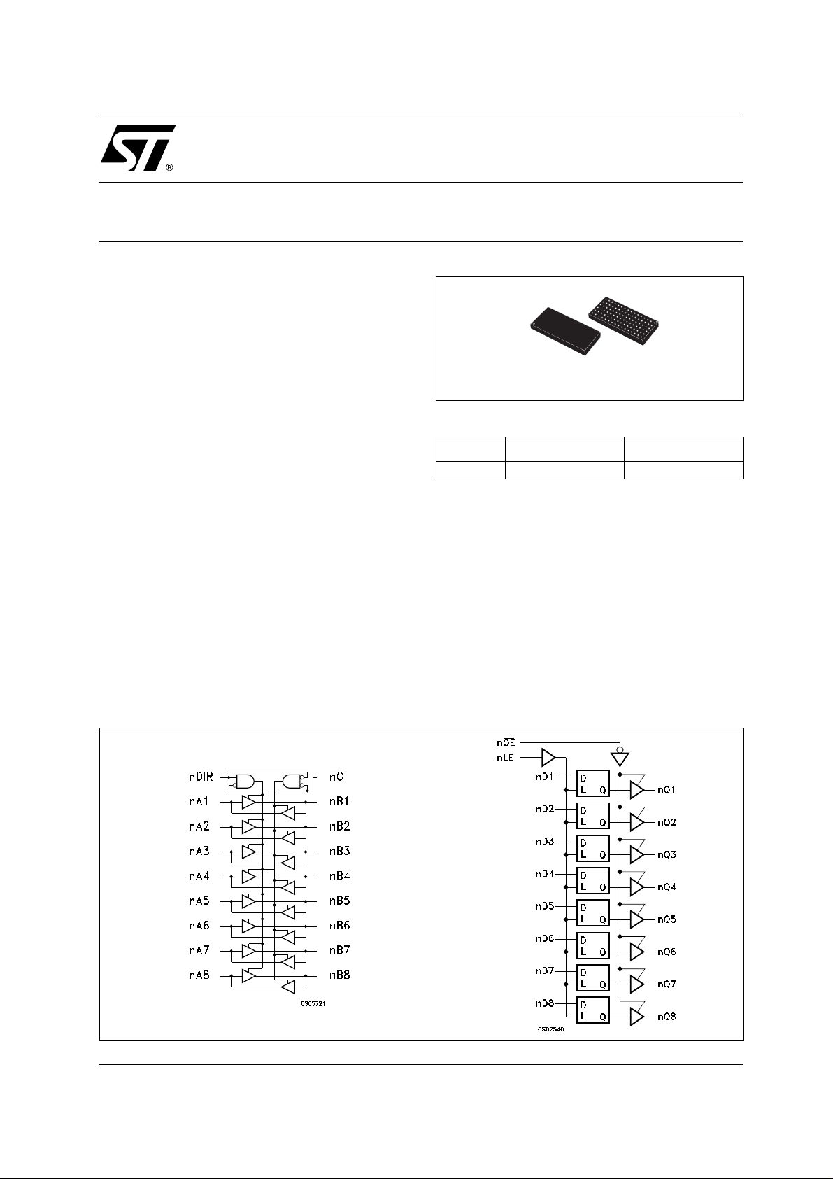
The 74ACT16244 is a low voltage CMOS 16-BIT
D-TYPE LATCHand 16 BIT BUS TRANSCEIVER
with 3-STATE ou tput non inverting fabricated with
sub-micron silicon gate and double-layer metal
wiring C
2
MOS technology.
Both functions can be used as 16 bit or dual octal
devices,so the 16 bittransceivercan be used ad 8
bit bus buffer plus 8 bit tran scei ver, or only 16 bit
buffer in selec t direction.
= 4.8ns (TYP.) at VCC=5V
PD
74ACT32701
PRELIMINARY DATA
LFBGA96
(Top and Bottom view)
ORDER CODES
PACKAGE TRAY T & R
LFBGA96 74ACT32701LB 74ACT32701LBR
This d ev ice can be used to integrate in one chip
the internal logic component required to S TV 0701
to work ad P.O.D. interface in Digital TV
application. It is ideal for low power and high
speed 4.5 to 5.5. applications.
All inputs and outputs are equipped with
protection circuits against st atic discharge, giving
them ESD immunity and transient excess voltage.
LOGIC DIAGRAM
1/9July 2003
This is preliminary information on a new product now in development are or undergoing evaluation. Details subject to change without notice.
Page 2
74ACT32701
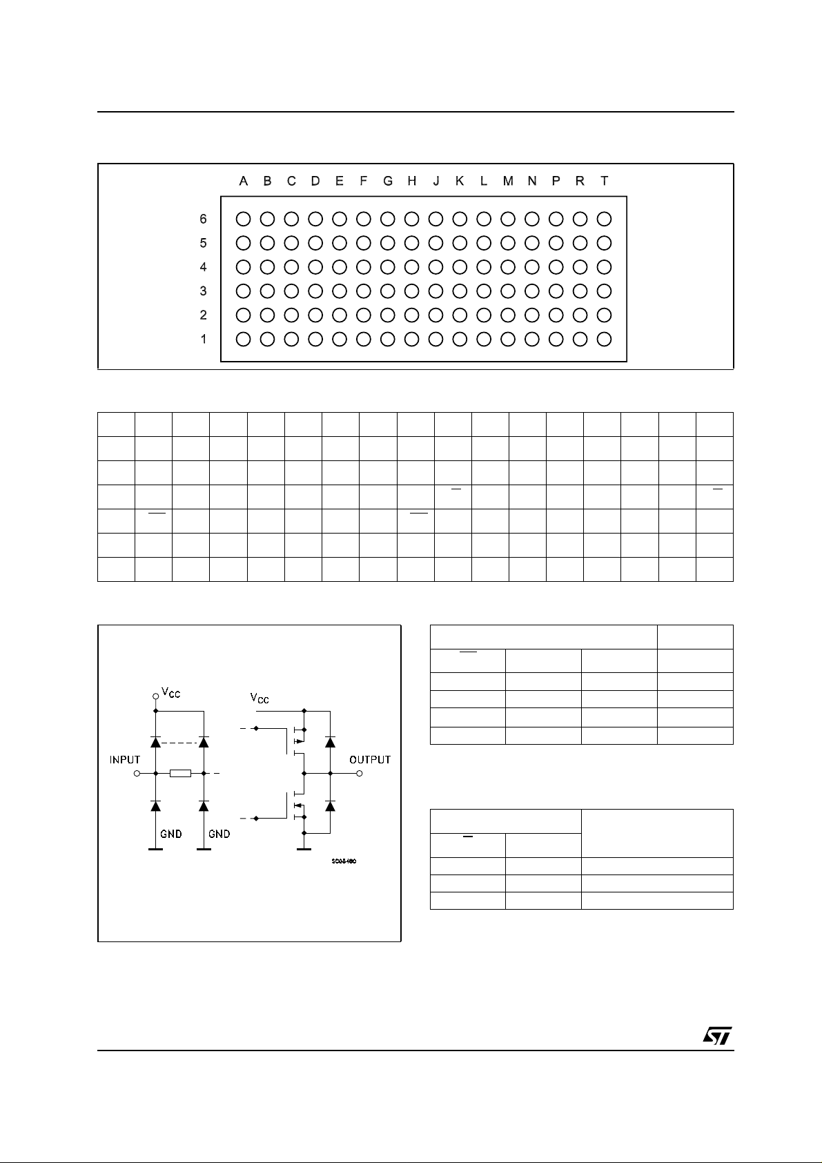
PIN CONNECTION (Top view)
TERMINAL ASSIGNMENT
ABCDEFGHJKLMNPRT
61D2 1D4 1D6 1D8 2D2 2D4 2D6 2D7 3A2 3A4 3A6 3A8 4A2 4A4 4A6 4A7
5 1D1 1D3 1D5 1D7 2D1 2D3 2D5 2D8 3A1 3A3 3A5 3A7 4A1 4A3 4A5 4A8
4 1LE GND
3 1OE GND
V
CC
V
CC
GND GND
GND GND
V
GND 2LE 3G GND
CC
V
GND 2OE 3DIR GND
CC
2 1Q1 1Q3 1Q5 1Q7 2Q1 2Q3 2Q5 2B8 3B1 3B3 3B5 3B7 4B1 4B3 4B5 4B8
V
CC
V
CC
GND GND
GND GND
V
CC
V
CC
GND 4G
GND 4DIR
1 1Q2 1Q4 1Q6 1Q8 2Q2 2Q4 2Q6 2B7 3B2 3B4 3B6 3B8 4B2 4B4 4B6 4B7
INPUT AND OUTPUT EQUIVALENT CIRCUIT TRUTH TABLE (e ac h 8bit section of 16bit Latch)
INPUTS OUTPUT
OE
LE D Q
LHHH
LHLL
LLX
Q
0
HXXZ
TRUTH TABLE (each 8bit s ection of 16bit
Transceiver)
INPUTS
G
DIR
L L B data to A bus
L H A data to B bus
H X Isolation
X : Don‘tCare
Z : High Impedance
OPERATION
2/9
Page 3
74ACT32701
ABSOLUTE MAXIMUM RATINGS
Symbol Parameter Value Unit
V
V
V
I
I
OK
I
or I
I
CC
T
T
Absolute Maximum Ratings are those values beyond which damage to the device may occur. Functional operation under these conditions is
not implied.
RECOMMENDED OPERATING CONDITIONS
Symbol Parameter Value Unit
V
V
V
T
dt/dv
1) VINfrom0.8V to 2.0V
Supply Voltage
CC
DC Input Voltage -0.5 to VCC+ 0.5
I
DC Output Voltage -0.5 to VCC+ 0.5
O
DC Input Diode Current
IK
DC Output Diode Current
DC Output Current
O
DC VCCor Ground Current
GND
Storage Temperature
stg
Lead Temperature (10 sec)
L
Supply Voltage
CC
Input Voltage 0 to V
I
Output Voltage 0 to V
O
Operating Temperature
op
Input Rise and Fall Time V
= 4.5 to 5.5V (note 1)
CC
-0.5 to +7 V
± 20 mA
± 20 mA
± 50 mA
± 400 mA
-65 to +150 °C
300 °C
4.5 to 5.5 V
CC
CC
-40 to 85 °C
8 ns/V
V
V
V
V
3/9
Page 4

74ACT32701
DC SPECIFICATIONS
Test Condition Value
Symbol Parameter
V
V
V
I
I
I
OHD
1) Maximum test duration 2ms, one output loaded at time
2) Incident wave switching is guaranteed on transmission lines with impedances as low as 50Ω
High Level Input Voltage 4.5
IH
V
Low Level Input Voltage 4.5
IL
High Level Output Voltage
OH
Low Level Output Voltage
OL
Input Leakage Current
I
I
High Impedance Output
I
OZ
Leakage Current
Max ICC/Input
CCT
Quiescent Supply Current
I
CC
OLD
Dynamic Output Current
(note 1, 2)
V
CC
(V)
= 0.1 V or VCC-0.1V
V
O
= 0.1 V or VCC-0.1V
V
5.5 0.8 0.8
4.5
5.5
4.5
5.5
4.5
5.5
4.5
5.5
5.5
5.5
5.5
5.5
5.5
O
IO=-50 µA
=-50 µA
I
O
=-24 mA
I
O
=-24 mA
I
O
IO=50 µA
=50 µA
I
O
=24 mA
I
O
=24 mA
I
O
VI=VCCor GND
VI=VIHor V
V
or GND
CC
VI=VCC- 2.1V
VI=VCCor GND
= 1.65 V max
V
OLD
V
= 3.85 V min.
OHD
VO=
IIL
Min. Typ. Max. Min. Max.
2.0 2.0
4.4 4.49 4.4
5.4 5.49 5.4
3.86 3.76
4.86 4.76
= 25°C
T
A
-40 to 85°C
0.8 0.8
0.001 0.1 0.1
0.001 0.1 0.1
0.36 0.44
0.36 0.44
± 0.1 ± 1 µA
± 0.5 ± 5 µA
0.9 1 mA
880µA
75 mA
-75 mA
Unit
V5.5 2.0 2.0
V
V
AC ELECTRICAL CHARACTERISTICS (CL=50pF,RL= 500 Ω, In put tr=tf=3ns)
Test Condition Value
= 25°C
Symbol Parameter
t
t
t
t
t
t
(*) Voltage range is5.0V ± 0.5V
Propagation Delay Time
PLH
PHL
Output Enable Time
PZL
PZH
Output Disable Time
PLZ
PHZ
V
(V)
5.0
5.0
5.0
CC
(*)
(*)
(*)
T
A
Min. Typ. Max. Min. Max.
2.0 3.3 5.0 2.0 6.0
3.0 4.8 6.5 3.0 8.0
4.0 6.5 8.7 4.0 9.7
3.0 5.5 7.7 3.0 8.8
4.0 6.0 8.0 4.0 9.2
3.0 4.6 6.4 3.0 7.3
-40 to 85°C
Unit
ns
ns
ns
4/9
Page 5

74ACT32701
CAPACITIVE CHARACTERISTICS
Test Condition Value
= 25°C
Symbol Parameter
V
CC
(V)
C
C
C
1) CPDis defined as the value of the IC’s internal equivalent capacitance which is calculated from the operating current consumption without
load. (Refer to Test Circuit). Average operating current can be obtained by the following equation. I
Input Capacitance
IN
Output Capacitance
OUT
Power Dissipation Capaci-
PD
tance (note 1)
5.0 3.6 pF
5.0 11 pF
= 10MHz
5.0
f
IN
T
A
Min. Typ. Max. Min. Max.
42 pF
CC(opr)=CPDxVCCxfIN+ICC
TEST CIRCUIT
-40 to 85°C
/n(percircuit)
Unit
Test Switch
t
PLH,tPHL
t
PZL,tPLZ
t
PZH,tPHZ
CL= 50pF or equivalent (includes jig and probe capacitance)
=500Ωor equivalent
R
L=R1
R
T=ZOUT
of pulse generator (typically 50Ω)
Open
2V
CC
GND
5/9
Page 6

74ACT32701
WAVEFORM 1: PROPAG ATION DE LAYS (f=1MHz; 50% duty cycle)
WAVEFORM 2: OUTPUT ENABLE AND DISABLE TIME (f=1MHz; 50% duty cycle)
6/9
Page 7

74ACT32701
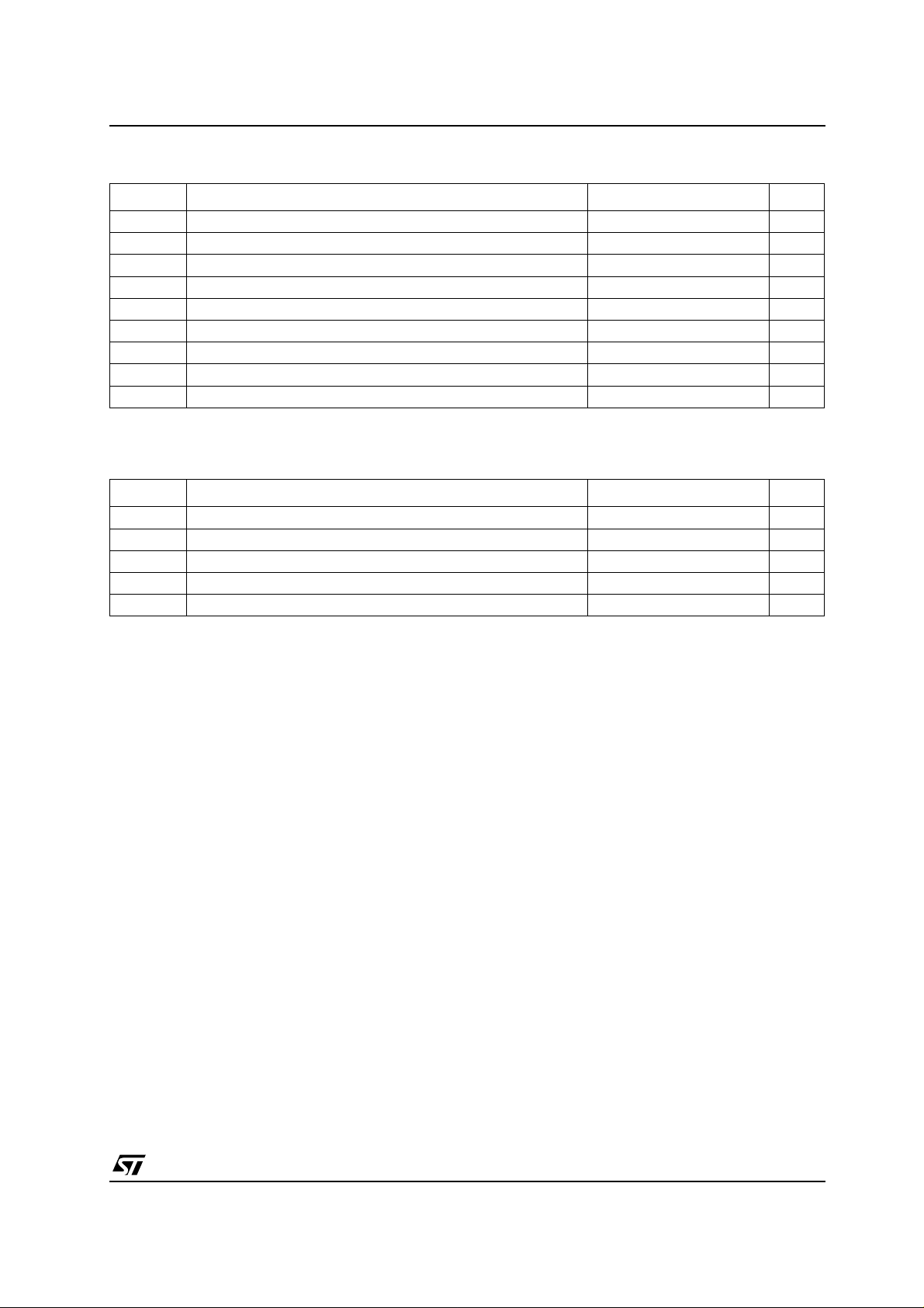
LFBGA96 MECHANICAL DATA
mm. mils
DIM.
A 13.40 13.60 527.5 535.4
B 5.40 5.60 212.6 220.5
C 1.6 63.0
D 0.5 19.7
E 0.8 31.5
F 0.85 33.5
MIN. TYP MAX. MIN. TYP. MAX.
7/9
Page 8

74ACT32701
Tape & Reel LFBGA96 MECHANICAL DATA
mm. inch
DIM.
MIN. TYP MAX. MIN. TYP. MAX.
A 330 12.992
C 12.8 13.2 0.504 0.519
D 20.2 0.795
N 60 2.362
T 30.4 1.196
Ao 5.8 6.0 0.228 0.236
Bo 13.8 14.0 0.543 0.551
Ko 2.1 2.3 0.083 0.091
Po 3.9 4.1 0.153 0.161
P 7.9 8.1 0.311 0.319
8/9
Page 9

74ACT32701
Information furnished is believed to be accurate and reliable. However, STMicroelectronics assumes no responsibility for the
consequences of use o f suc h inf ormat ion n or f or an y infr ingeme nt of paten ts or oth er ri gh ts of third part ies whic h may resul t f rom
its use. No license is granted by implication or otherwise under any patent or patent rights of STMicroelectronics. Specifications
mentioned in this publication are subject to change without notice. This publication supersedes and replaces all information
previously supplied. STMicroelectronics products are not authorized for use as critical components in life support devices or
systems without express written approval of STMicroelectronics.
Australia - Brazil - Canada - China - Finland - France - Germany - Hong Kong - India - Israel - Italy - Japan - Malaysia - Malta - Morocco
© The ST logo is a registered trademark of STMicroelectronics
© 2003 STMicroelectronics - Printed in Italy - All Rights Reserved
STMicroelectronics GROUP OF COMPANIES
Singapore - Spain - Sweden - Switzerland - United Kingdom - United States.
© http://www.st.com
9/9
 Loading...