

Page 1
74ACT280
9 BIT PARITY GENERATOR/CHECKER
■ HIGHSPEED:t
■
LOW POWERDISSIPATION:
I
=4 µA (MAX.) atTA=25oC
CC
■
COMPATIBLEWITHTTLOUTPUTS
V
=2V(MIN),VIL=0.8V(MAX)
IH
■ 50Ω TRANSMISSIONLINEDRIVING
=4ns(TYP.)atVCC=5V
PD
CAPABILITY
■ SYMMETRICALOUTPUTIMPEDANCE:
|I
|=IOL=24mA (MIN)
OH
■ BALANCEDPROPAGATIONDELAYS:
t
≅ t
PLH
PHL
■
OPERATINGVOLT AGERANGE:
V
(OPR)= 4.5 Vto 5.5V
CC
■ PINANDFUNCTIONCOMPATIBLEWITH
74SERIES280
■ IMPROVEDLATCH-UPIMMUNITY
DESCRIPTION
The AC280 is an advanced high-speed CMOS 9
BIT PARITY GENERATOR - CHECKER
fabricated with sub-micron silicon gate and
double-layermetal wiring C
2
MOS technology.It is
ideal for low power applications mantaining high
speed operation similar to eqivalent Bipolar
SchottkyTTL.
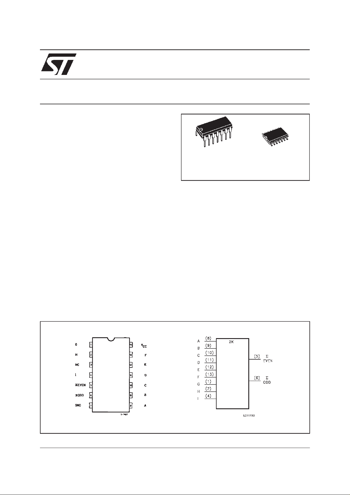
It is composed of nine data inputs (A to I) and
odd/evenparity outputs(ΣODD andΣEVEN).The
B
(PlasticPackage)
(Micro Package)
M
ORDERCODES :
74ACT280B 74ACT280M
nine data inputs control the output conditions.
When the number of high level input is odd,
ΣODD output is kept high and ΣEVEN outputlow.
Conservely, when the output is even,ΣEVEN
output is kept high and ΣODD low.
The IC generates either odd or even parity
makingit flexibleapplication.
The word-length capability is easily expanded by
cascading.
The device is designed to interface directly High
Speed CMOS systems with TTL, NMOS and
CMOSoutput voltage levels.
All inputs and outputs are equipped with
protection circuits against static discharge, giving
them 2KV ESD immunity and transient excess
voltage.
PIN CONNECTION AND IEC LOGICSYMBOLS
December 1998
1/8
Page 2
74ACT280
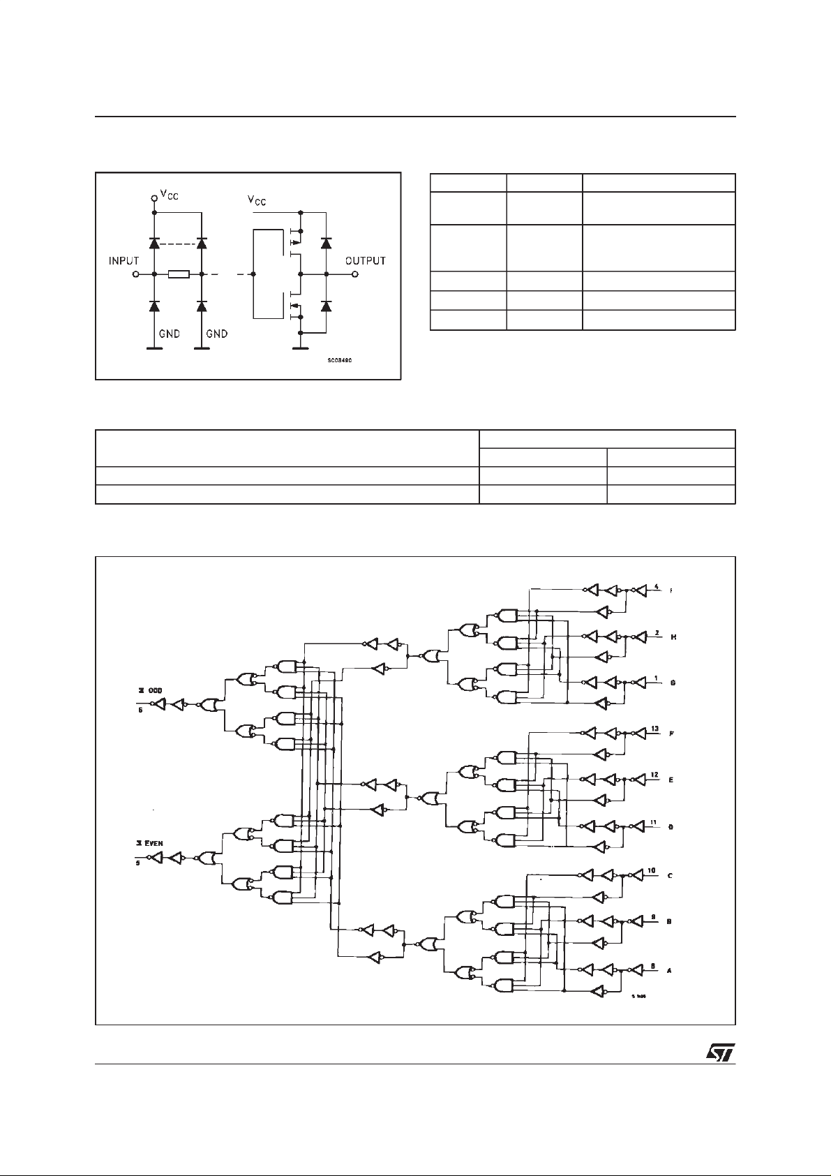
INPUT AND OUTPUT EQUIVALENTCIRCUIT
TRUTH TABLE
NUMB E R OF INP UT A TRHU I THAT ARE HIGH OUT P UT
0, 2, 4, 6, 8 H L
1, 3, 5, 7, 9 L H
LOGICDIAGRAM
PIN DESCRIPTION
PI N No SYMB OL NAME AND FUNCT I O N
5, 6
8, 9, 10, 11,
12, 13, 1, 2,
4
3 NC No Connection
7 GND Ground (0V)
14 V
EVEN
Σ
ΣODD
A to I Data Inputs
CC
EVEN
Σ
Parity Outputs
Positive Supply Voltage
ODD
Σ
2/8
Page 3
74ACT280
ABSOLUTE MAXIMUM RATINGS
Symb o l Para met er Val u e Uni t
V
V
V
I
I
OK
I
or I
I
CC
T
T
AbsoluteMaximumRatingsarethosevaluesbeyond whichdamagetothedevicemayoccur.Functionaloperationunderthese condition isnotimplied.
RECOMMENDED OPERATINGCONDITIONS
Symb o l Parameter Val u e Uni t
V
V
V
T
dt/dv Input Rise and Fall Time V
1)VINfrom0.8V to2.0V
Supply Voltage -0.5 to +7 V
CC
DC Input Voltage -0.5 to VCC+ 0.5 V
I
DC Output Voltage -0.5 to VCC+ 0.5 V
O
DC Input Diode Current ± 20 mA
IK
DC Output Diode Current ± 20 mA
DC Output Current
O
DC VCCor Ground Current
GND
Storage Temperature -65 to +150
stg
Lead Temperature (10 sec) 300
L
Supply Voltage 4.5 to 5.5 V
CC
Input Voltage 0 to V
I
Output Voltage 0 to V
O
Operating Temperature: -40 to +85
op
= 4.5 to 5.5V (note 1) 8 ns/V
CC
50 mA
±
200 mA
±
CC
CC
o
C
o
C
V
V
o
C
DC SPECIFICATIONS
Symbol Parameter Test Conditions Value Unit
=25oC -40 to 85oC
V
CC
(V)
High Level Input Voltage 4.5 VO= 0.1V or
V
IH
5.5 2.0 1.5 2.0
Low Level Input Voltage 4.5 VO= 0.1V or
V
IL
5.5 1.5 0.8 0.8
High Level Output
V
OH
Voltage
4.5
5.5 I
4.5 I
5.5 I
Low Level Output
V
OL
Voltage
4.5
5.5 I
4.5 I
5.5 I
Input Leakage Current 5.5 VI=VCCor GND ±0.1 ±1 µA
I
I
Max ICC/Input 5.5 VI=VCC-2.1V 0.6 1.5 mA
I
CCT
Quiescent Supply
I
CC
5.5 VI=VCCor GND 4 40
V
-0.1 V
CC
V
-0.1 V
CC
IO=-50 µA 4.4 4.49 4.4
(*)
=
V
I
V
IH
V
IL
(*)
V
I
V
IH
V
IL
=-50 µA 5.4 5.49 5.4
O
or
=-24 mA 3.86 3.76
O
=-24 mA 4.86 4.76
O
IO=50µA 0.001 0.1 0.1
=
=50 mA 0.001 0.1 0.1
O
or
=24 mA 0.36 0.44
O
=24 mA 0.36 0.44
O
Current
Dynamic Output Current
I
OLD
OHD
(note 1, 2)
I
1) Maximum test duration 2ms, one output loaded attime
2)Incident waveswitchingisguaranteed on transmissionlines withimpedances aslowas 50Ω.
5.5 V
= 1.65 V max 75 mA
OLD
V
= 3.85 V min -75 mA
OHD
T
A
Min. Typ. Max. Min. Max.
2.0 1.5 2.0
1.5 0.8 0.8
µ
V
V
V
V
A
3/8
Page 4

74ACT280
AC ELECTRICALCHARACTERISTICS
= 50 pF, RL= 500 Ω, Input tr=tf=3 ns)
(C
L
Symbol Parameter Test Conditio n Value Unit
t
Propagation Delay Time
PLH
t
PHL
(Input -ΣODD, ΣEVEN)
(*) Voltagerangeis5V± 0.5V
V
(V)
5.0
CC
(*)
T
=25oC -40 to 85oC
A
Min. Typ. Max. Min. Max.
3.0 8.5 13.0 2.0 14.5
ns
CAPACITIVE CHARACTERISTICS
Symbol Parameter Test Conditions Value Unit
T
=25oC -40 to 85oC
A
Min. Typ. Max. Min. Max.
4
pF
Input Capacitance
C
IN
Power Dissipation
C
PD
V
CC
(V)
5.0
5.0 75 pF
Capacitance (note 1)
1)CPDisdefinedasthevalueoftheIC’sinternal equivalent capacitance whichiscalculated fromtheoperatingcurrentconsumption withoutload.(Referto
TestCircuit).Averageoperatingcurrent canbeobtainedbythefollowingequation.I
(opr)=CPD• VCC• fIN+I
CC
CC
TESTCIRCUIT
= 50pF or equivalent(includes jigand probe capacitance)
C
L
R
=500Ωorequivalent
L=R1
R
ofpulsegenerator(typically50Ω)
T=ZOUT
4/8
Page 5

74ACT280
WAVEFORM:PROPAGATIONDELAYS
(f=1MHz;50% duty cycle)
5/8
Page 6

74ACT280
Plastic DIP-14 MECHANICAL DATA
DIM.
MIN. TYP. MAX. MIN. TYP. MAX.
a1 0.51 0.020
B 1.39 1.65 0.055 0.065
b 0.5 0.020
b1 0.25 0.010
D 20 0.787
E 8.5 0.335
e 2.54 0.100
e3 15.24 0.600
F 7.1 0.280
I 5.1 0.201
L 3.3 0.130
Z 1.27 2.54 0.050 0.100
mm inch
6/8
P001A
Page 7

SO-14 MECHANICALDATA
74ACT280
DIM.
MIN. TYP. MAX. MIN. TYP. MAX.
A 1.75 0.068
a1 0.1 0.2 0.003 0.007
a2 1.65 0.064
b 0.35 0.46 0.013 0.018
b1 0.19 0.25 0.007 0.010
C 0.5 0.019
c1 45 (typ.)
D 8.55 8.75 0.336 0.344
E 5.8 6.2 0.228 0.244
e 1.27 0.050
e3 7.62 0.300
F 3.8 4.0 0.149 0.157
G 4.6 5.3 0.181 0.208
L 0.5 1.27 0.019 0.050
M 0.68 0.026
S 8 (max.)
mm inch
P013G
7/8
Page 8

74ACT280
Information furnished is believed to be accurate and reliable. However, STMicroelectronics assumes no responsibility for the consequences
of use of such information nor for any infringement of patents or other rights of third parties which may result from its use. No license is
granted by implication or otherwise under any patent or patent rights of STMicroelectronics. Specification mentioned in this publication are
subject to change without notice. This publication supersedes and replaces all information previously supplied. STMicroelectronics products
are not authorized foruse as critical components inlife support devices or systems without express written approval of STMicroelectronics.
The ST logo is a registered trademark of STMicroelectronics
1998 STMicroelectronics – Printed in Italy – All Rights Reserved
STMicroelectronics GROUP OF COMPANIES
Australia - Brazil - Canada -China -France -Germany - Italy - Japan - Korea - Malaysia - Malta - Mexico -Morocco -The Netherlands -
Singapore - Spain -Sweden - Switzerland - Taiwan - Thailand - UnitedKingdom - U.S.A.
http://www.st.com
.
8/8
 Loading...