

Page 1
OCTAL D-TYPE FLIP FLOP WITH CLEAR
■ HIGHSPEED:
=190MHzns(TYP.)atVCC=5V
f
MAX
■ LOW POWER DISSIPATION:
I
=8µA (MAX.)at TA=25oC
CC
■ COMPATIBLEWITHTTLOUTPUTS
V
=2V(MIN),VIL=0.8V(MAX)
IH
■
50ΩTRANSMISSIONLINEDRIVING
CAPABILITY
■ SYMMETRICALOUTPUTIMPEDANCE:
|I
|=IOL=24mA(MIN)
OH
■ BALANCEDPROPAGATIONDELAYS:
≅
t
t
PLH
PHL
■ OPERATINGVOLTAGERANGE:
V
(OPR)= 4.5Vto 5.5V
CC
■ PINANDFUNCTION COMPATIBLEWITH
74SERIES273
■
IMPROVEDLATCH-UP IMMUNITY
DESCRIPTION
The ACT273 is a high-speed CMOS OCTAL
D-TYPE FLIP FLOP WITH CLEAR fabricated
with sub-micron silicon gate and double-layer
metal wiring C
power applications mantaining high speed
operation similar to equivalent Bipolar Schottky
TTL.
2
MOS technology.It is ideal for low
74ACT273
PRELIMINARY DATA
M
B
(PlasticPackage)
ORDER CODES :
74ACT273B
74ACT273M
74ACT273T
Information signals applied to D inputs are
transfered to the Q output on the positive going
edgeof theclock pulse.
Whenthe CLEAR input is held low, the Q outputs
are held low independentelyof the otherinputs .
The device is designed to interface directly High
Speed CMOS systems with TTL, NMOS and
CMOSoutput voltagelevels.
All inputs and outputs are equipped with
protection circuits against static discharge, giving
them 2KV ESD immunity and transient excess
voltage.
(Micro Package)
T
(TSSOPPackage)
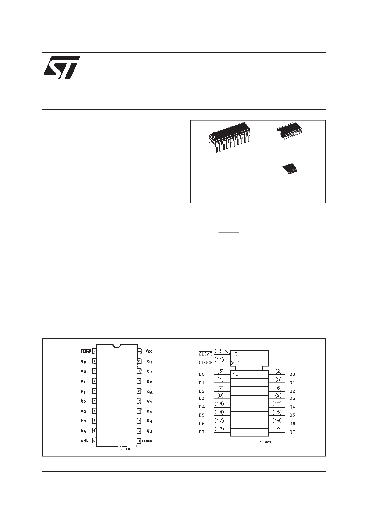
PIN CONNECTION AND IEC LOGICSYMBOLS
May 1999
1/11
Page 2
74ACT273
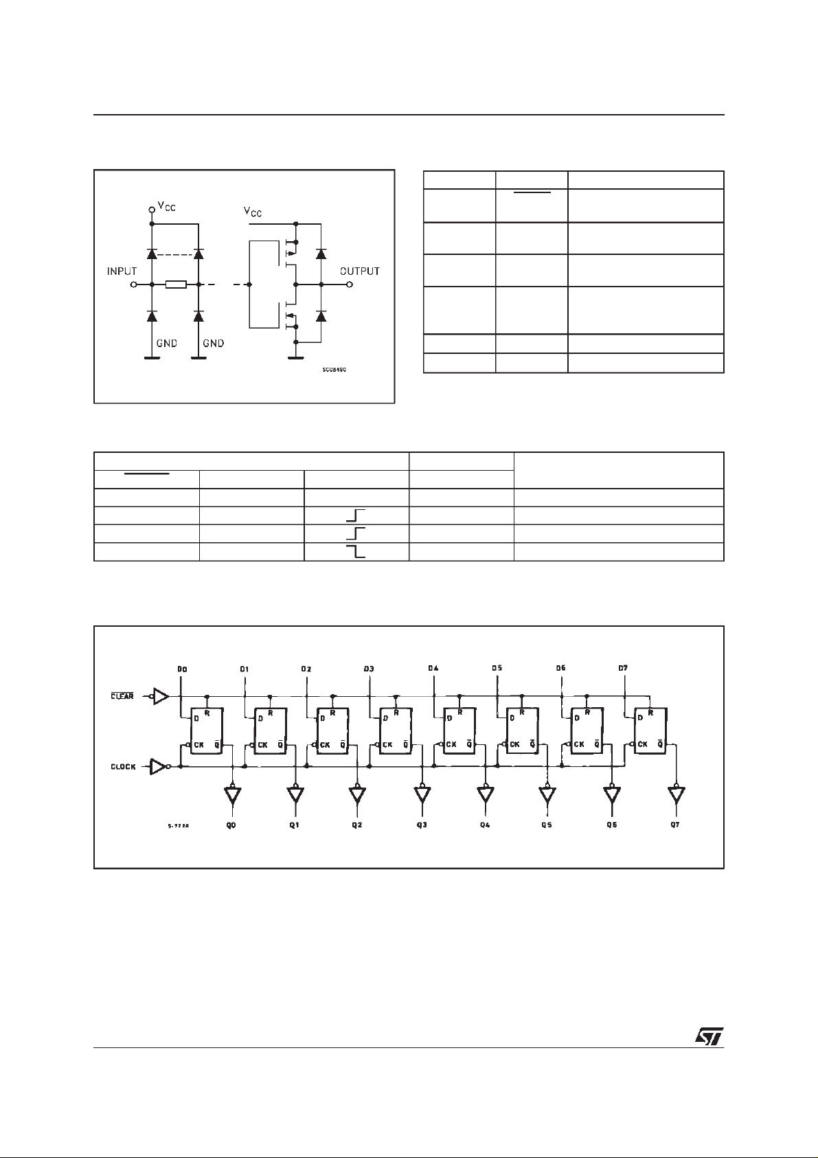
INPUT AND OUTPUTEQUIVALENTCIRCUIT
TRUTH TABLE
INPUTS OUTPUTS FUNCTION
CLE AR D CLOCK Q
L X X L CLEAR
HL L
HH H
HX Q
X:Don’tCare
PIN DESCRIPTION
PI N No SYM BO L NAM E AND F U NCTIO N
1 CLEAR Asyncronous Master
Reset (Active LOW)
2,5,6,9,12,
15, 16,19
3,4,7,8,13,
14, 17,18
11 CLOCK Clock Input
10 GND Ground (0V)
20 V
n
Q0toQ7 Flip-Flop Outpus
D0toD7 Data Inputs
(LOW-to-HIGH, EdgeTriggered)
Positive Supply Voltage
CC
NOCHANGE
LOGICDIAGRAMS
Thislogic diagram has notbeused to esimate propagation delays
2/11
Page 3
74ACT273
ABSOLUTE MAXIMUM RATINGS
Symb o l Para met er Val u e Uni t
V
V
V
I
I
OK
I
orI
I
CC
T
T
AbsoluteMaximumRatingsarethosevaluesbeyond whichdamagetothedevicemayoccur. Functionaloperationundertheseconditionisnotimplied.
RECOMMENDED OPERATINGCONDITIONS
Symb o l Parameter Val u e Uni t
V
V
V
T
dt/dv Input Rise and Fall Time V
1)VINfrom0.8Vto 2.0V
Supply Voltage -0.5to+7 V
CC
DC Input Voltage -0.5toVCC+0.5 V
I
DC Output Voltage -0.5toVCC+0.5 V
O
DC Input Diode Current ±20 mA
IK
DC Output Diode Current ±20 mA
DC Output Current
O
DC VCCor Ground Current
GND
Storage Temperature -65to+150
stg
Lead Temperature (10 sec) 300
L
Supply Voltage 4.5to5.5 V
CC
Input Voltage 0toV
I
Output Voltage 0toV
O
Operating Temperature: -40to+85
op
= 4.5 to 5.5V (note 1) 8 ns/V
CC
50 mA
±
400 mA
±
CC
CC
o
C
o
C
V
V
o
C
3/11
Page 4
74ACT273
DC SPECIFICATIONS
Symbol Parameter Test Conditi ons Value Un it
T
V
CC
(V)
High Level Input Voltage 4.5 VO=0.1Vor
V
IH
5.5 2.0 1.5 2.0
Low Level Input Voltage 4.5 VO=0.1Vor
V
IL
5.5 1.5 0.8 0.8
High Level Output
V
OH
Voltage
4.5
5.5 I
V
V
4.5 I
5.5 I
Low Level Output
V
OL
Voltage
4.5
5.5 I
V
V
4.5 I
5.5 I
Input Leakage Current 5.5 VI=VCCorGND ±0.1 ±1 µA
I
I
Max ICC/Input 5.5 VI=VCC-2.1V 0.6 1.5 mA
I
CCT
Quiescent Supply
I
CC
5.5 VI=VCCorGND 4 40
-0.1V
V
CC
V
-0.1V
CC
IO=-50µA 4.4 4.49 4.4
(*)
=
I
or
IH
V
IL
(*)
I
or
IH
V
IL
=-50µA 5.4 5.49 5.4
O
=-24 mA 3.86 3.76
O
=-24 mA 4.86 4.76
O
IO=50µA 0.001 0.1 0.1
=
=50mA 0.001 0.1 0.1
O
=24mA 0.36 0.44
O
=24mA 0.36 0.44
O
Current
Dynamic Output Current
I
OLD
(note 1, 2)
I
OHD
1) Maximumtest duration 2ms, one output loaded at time
2)Incidentwaveswitchingis guaranteedontransmissionlineswithimpedances aslowas50Ω.
5.5 V
=1.65V max 75 mA
OLD
V
=3.85Vmin -75 mA
OHD
=25oC -40 to 85oC
A
Min. Typ. Max. Min. Max.
2.0 1.5 2.0
1.5 0.8 0.8
µ
V
V
V
V
A
4/11
Page 5

74ACT273
AC ELECTRICAL CHARACTERISTICS
= 50 pF, RL= 500 Ω, Input tr=tf=3 ns)
(C
L
Symbol Parameter Test Conditio n Value Un it
t
Propagation Delay Time
PLH
t
CK to Q
PHL
Propagation Delay Time
t
PLH
CLR to Q
t
PHL
CLR pulse Width, LOW 5.0
t
wL
CK pulse Width 5.0
t
w
Setup Time Q to CK
t
s
HIGH or LOW
Hold Time Q to CK
t
h
HIGH or LOW
Recovery Time CLR to
t
REM
CK
Maximum Clock
f
MAX
Frequency
(*) Voltagerangeis 5V± 0.5V
V
(V)
5.0
5.0
5.0
5.0
5.0
5.0
CC
(*)
(*)
(*)
(*)
(*)
(*)
(*)
(*)
T
=25oC -40 to 85oC
A
Min. Typ. Max. Min. Max.
1.5 6.5 8.5 1.5 9.0
1.5 7.0 9.0 1.5 9.5
1.5 4.0 4.0 ns
1.0 4.0 4.0
1.0 3.5 3.5
-0.5 1.5 1.5
0.5 3.0 3.0
125 190 110
ns
ns
ns
ns
ns
ns
MHz
CAPACITIVE CHARACTERISTICS
Symbol Parameter Test Conditi ons Value Un it
V
CC
(V)
Input Capacitance 5.0 4 pF
C
IN
Power Dissipation
C
PD
5.0 fIN=10 MHz 32 pF
Capacitance (note 1)
1)CPDisdefined asthevalueoftheIC’sinternalequivalentcapacitance whichiscalculatedfromtheoperatingcurrentconsumption withoutload.(Referto
TestCircuit).Averageopertingcurrentcanbeobtainedbythefollowingequation.I
(opr)=CPD• VCC• fIN+ICC/n(percircuit)
CC
=25oC -40 to 85oC
T
A
Min. Typ. Max. Min. Max.
5/11
Page 6

74ACT273
TESTCIRCUIT
CL= 50 pF or equivalent (includes jigand probe capacitance)
R
=500Ω orequivalent
L=R1
R
WAVEFORM1: PROPAGATIONDELAYS,SETUP ANDHOLD TIMES(f=1MHz; 50% duty cycle)
ofpulsegenerator (typically50Ω)
T=ZOUT
6/11
Page 7

74ACT273
WAVEFORM2: PROPAGATIONDELAYS
(f=1MHz;50% duty cycle)
WAVEFORM3: RECOVERYTIME (f=1MHz;50% duty cycle)
7/11
Page 8

74ACT273
Plastic DIP-20 (0.25) MECHANICAL DATA
DIM.
MIN. TYP. MAX. MIN. TYP. MAX.
a1 0.254 0.010
B 1.39 1.65 0.055 0.065
b 0.45 0.018
b1 0.25 0.010
D 25.4 1.000
E 8.5 0.335
e 2.54 0.100
e3 22.86 0.900
F 7.1 0.280
I 3.93 0.155
L 3.3 0.130
Z 1.34 0.053
mm inch
8/11
P001J
Page 9

SO-20 MECHANICALDATA
74ACT273
DIM.
MIN. TYP. MAX. MIN. TYP. MAX.
A 2.65 0.104
a1 0.10 0.20 0.004 0.007
a2 2.45 0.096
b 0.35 0.49 0.013 0.019
b1 0.23 0.32 0.009 0.012
C 0.50 0.020
c1 45 (typ.)
D 12.60 13.00 0.496 0.512
E 10.00 10.65 0.393 0.419
e 1.27 0.050
e3 11.43 0.450
F 7.40 7.60 0.291 0.299
L 0.50 1.27 0.19 0.050
M 0.75 0.029
S 8 (max.)
mm inch
P013L
9/11
Page 10

74ACT273
TSSOP20 MECHANICAL DATA
DIM.
mm inch
MIN. TYP. MAX. MIN. TYP. MAX.
A 1.1 0.433
A1 0.05 0.10 0.15 0.002 0.004 0.006
A2 0.85 0.9 0.95 0.335 0.354 0.374
b 0.19 0.30 0.0075 0.0118
c 0.09 0.2 0.0035 0.0079
D 6.4 6.5 6.6 0.252 0.256 0.260
E 6.25 6.4 6.5 0.246 0.252 0.256
E1 4.3 4.4 4.48 0.169 0.173 0.176
e 0.65 BSC 0.0256 BSC
K0
o
o
4
o
8
o
0
o
4
8
L 0.50 0.60 0.70 0.020 0.024 0.028
o
A
PIN 1 IDENTIFICATION
10/11
A2
A1
b
e
K
c
L
E
D
E1
1
Page 11

74ACT273
Information furnished is believed to beaccurate and reliable. However, STMicroelectronics assumes no responsibility forthe consequences
of use of such information nor for any infringement of patents or other rights of third parties which may result from its use. No license is
granted by implication or otherwise under any patent or patent rights of STMicroelectronics. Specification mentioned in thispublication are
subject tochange without notice. Thispublication supersedes and replaces all information previously supplied. STMicroelectronics products
are not authorized for use as critical components in life support devices or systems without express written approval of STMicroelectronics.
The ST logo is a trademark of STMicroelectronics
1999 STMicroelectronics – Printed in Italy –All Rights Reserved
STMicroelectronics GROUP OF COMPANIES
Australia - Brazil - Canada - China -France -Germany - Italy - Japan -Korea - Malaysia -Malta - Mexico - Morocco -The Netherlands -
Singapore - Spain -Sweden - Switzerland- Taiwan - Thailand - UnitedKingdom -U.S.A.
http://www.st.com
.
11/11
 Loading...