

Page 1
February 1989
Revised January 1999
74ACT2708 64 x 9 First-In, First-Out Memory
© 1999 Fairchild Semiconductor Corporation DS010144.prf www.fairchildsemi.com
74ACT2708
64 x 9 First-In, First-Out Memory
General Description
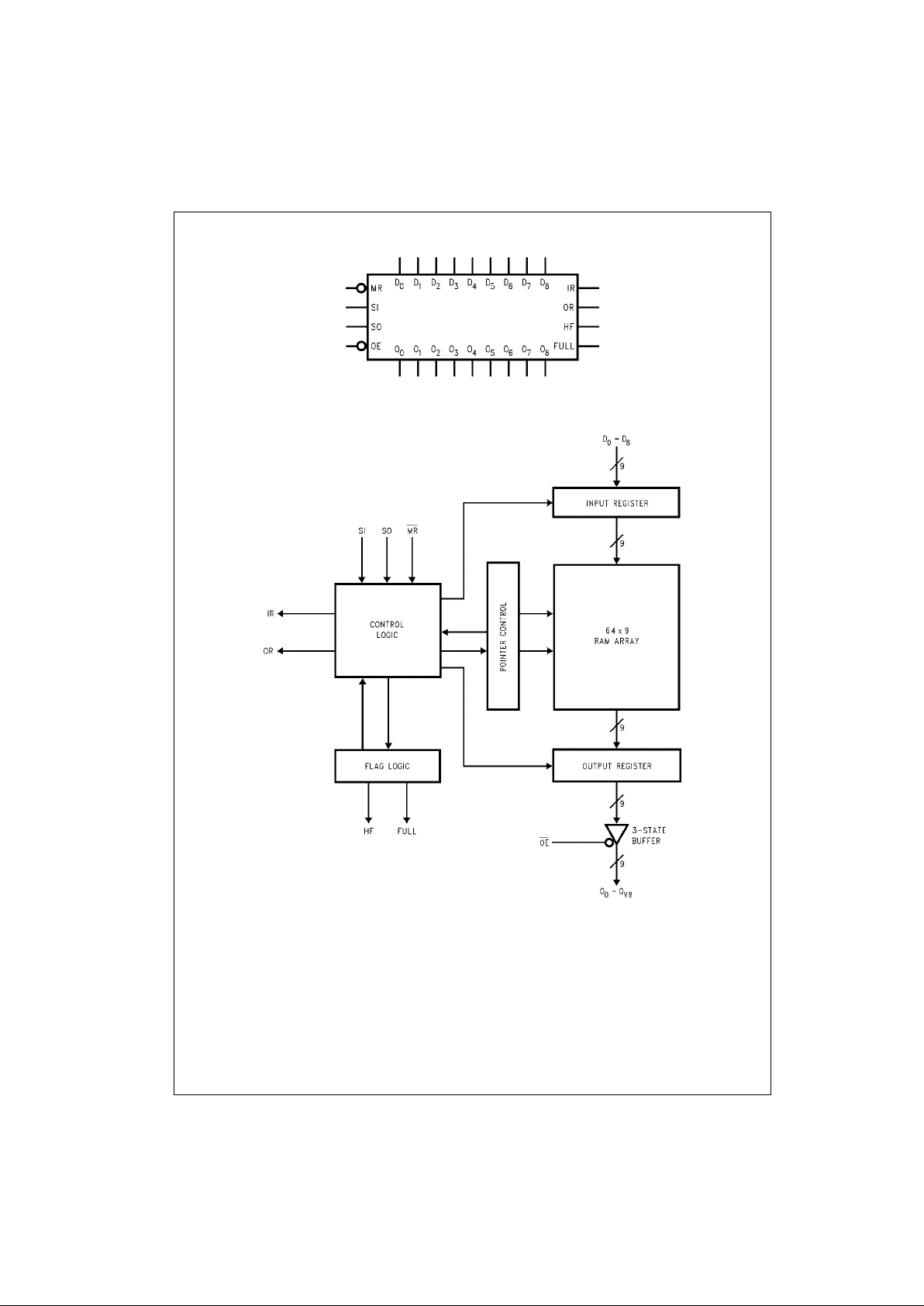
The ACT2708 is an exp andable first-in, first-out memor y
organized as 64 words by 9 bits. An 85 MHz shift-in and 60
MHz shift-out typical data rate makes it ideal for high-speed
applications. It uses a dual port RAM architecture with
pointer logic to achi eve the high speed with ne gligible fallthrough time.
Separate Shift-In (SI) and Shift -Ou t (S O) clocks cont rol t he
use of synchronous or asynchr onous write or re ad. Other
controls include a Mas ter Reset (MR
) and Output Enable
(OE
) for initializing the internal registers and allowing the
data outputs to be 3-S TATE. Input Ready (I R) and Output
Ready (OR) signal when the FIFO is ready for I/O operations. The status flags HF and FULL indicate when the
FIFO is full, empty or half full.
The FIFO can be expanded to provide different word
lengths by tying off unused data inputs.
Features
■ 64-words by 9-bit dual port RAM organization
■ 85 MHz shift-in, 60 MHz shift-out data rate, typical
■ Expandable in word width only
■ TTL-compatible inputs
■ Asynchronous or synchronous operation
■ Asynchronous master reset
■ Outputs source/sink 8 mA
■ 3-STATE outputs
■ Full ESD protection
■ Input and output pi ns directly in line for easy boar d lay-
out
■ TRW 1030 work-alike operation
Applications
• High-speed disk or tape controllers
• A/D output buffers
• High-speed graphics pixel buffer
• Video time base correction
• Digital filtering
Ordering Code:
Device also available in Tape and Reel. Specify by appendin g s uf f ix let te r “X” to the ordering cod e.
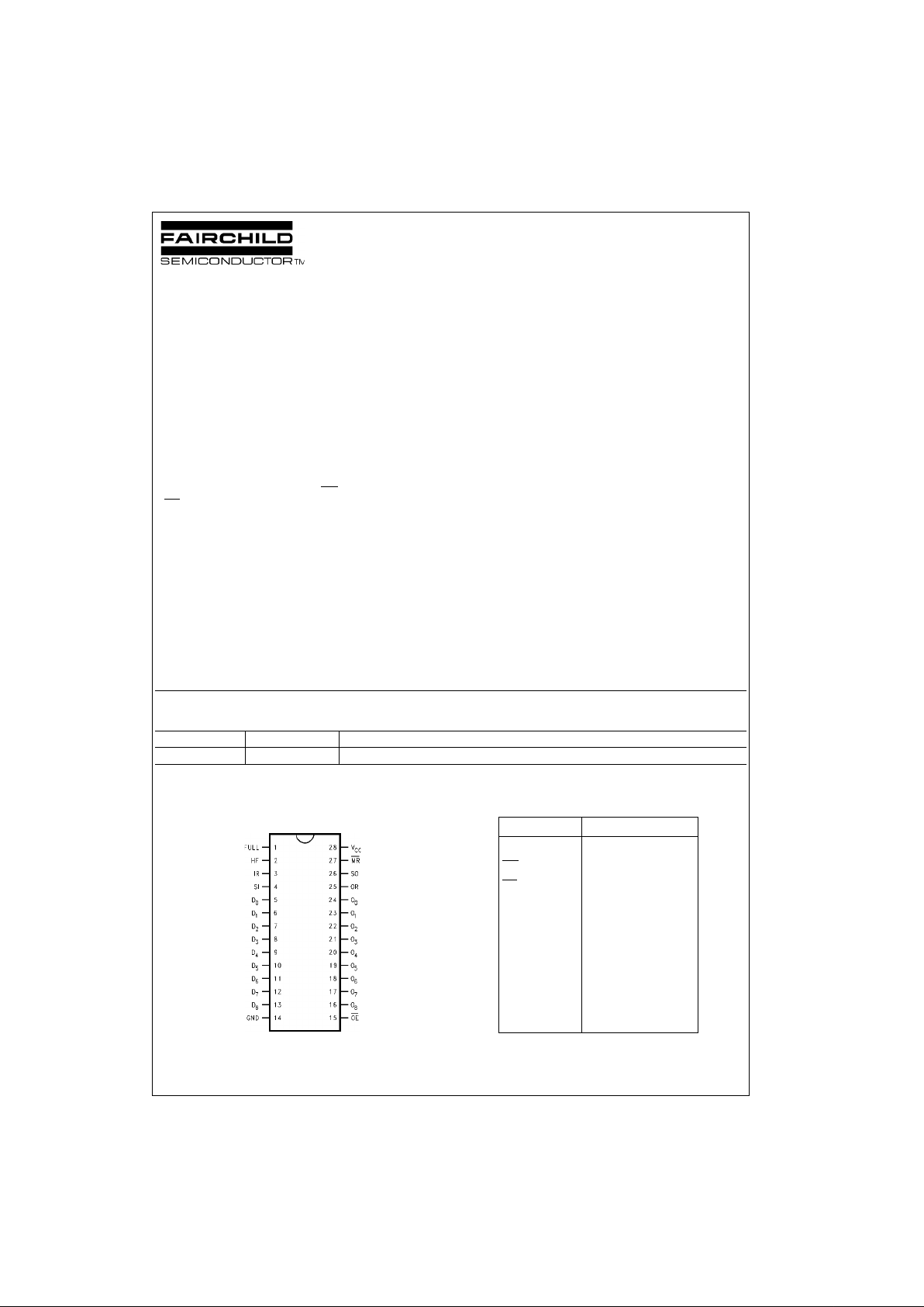
Connection Diagram
Pin Assignment for DIP
Pin Descriptions
FACT is a tra demark of Fairchild Semico nductor Corporation.
Order Number Package Number Package Description
74ACT2708PC N28B 28-Lead Plastic Dual-In-Line Package (PDIP), JEDEC MS-010, 0.600” Wide
Pin Names Description
D
0–D8
Data Inputs
MR
Master Reset
OE
Output Enable Input
SI Shift-In
SO Shift-Out
IR Input Ready
OR Output Ready
HF Half Full Flag
FULL Full Flag
O
0–O8
Data Outputs
Page 2
www.fairchildsemi.com 2
74ACT2708
Logic Symbol
Block Diagram
Page 3
3 www.fairchildsemi.com
74ACT2708
Functional Description
INPUTS
Data Inputs (D0–D8)
Data inputs for 9-bit wide d ata are TTL-compatible. Word
width can be reduced by tryin g unused inputs to ground
and leaving the corresponding outputs open.
Reset (MR
)
Reset is accomplished by pulsing th e MR
input LOW. Dur-
ing normal operation MR
is HIGH. A reset is requir ed aft er
power up to guarantee correct operation. On reset, the
data outputs go LOW, IR goes HIGH, OR goes LOW, FH
and FULL go LOW. During reset, both inter nal read and
write pointers are set to the first location in the array.
Shift-In (SI)
Data is written into the FIFO by pulsing SI HIGH. When
Shift-In goes HIGH, the data is l oad ed in to an i nte r n al da ta
latch. Data setup and hold times need to be adhered to
with respect to the falling edge of SI. The write cycle is
complete after the falling edge of SI. The shift-in is independent of any ongoing shift-out operation. After the first
word has been written in to the FIFO, the falling ed ge of SI
makes HF go HIGH, indicating a non-empty FIFO. The first
data word appears at the output after the falling edge of SI.
After half the memor y is filled, the next rising edge of SI
makes FULL go HIGH indicating a half-full FIFO. When the
FIFO is full, any further shift-ins are disabled.
When the FIFO is em pty and OE
is LOW, the falling edge
of the first SI will cause the first data word just shifted-in to
appear at the output, even though SO may be LOW.
Shift-Out (SO)
Data is read from the FIFO by the Shift-Out signal provided
the FIFO is not empty. SO going HIGH causes OR to go
LOW indicating that output stage is busy. On the falling
edge of SO, new data reaches the output after propagation
delay t
D
. If the last data has been shifted-o ut of the mem -
ory, OR continues to remain LOW, and the last word
shifted-out remains on the output pins.
Output Enable (OE
)
OE
LOW enables the 3-STATE output buffers. When OE is
HIGH, the outputs are in a 3-STATE mode.
OUTPUTS
Data Outputs (O0–O8)
Data outputs are enabled when OE
is LOW and in the 3-
STATE condition when OE
is HIGH.
Input Ready (IR)
IR HIGH indicates data can be shifted-in . When SI goes
HIGH, IR goes LOW, indicating input stage is busy. IR
stays LOW when the FIFO is full and goes HIGH after the
falling edge of the first shift-out.
Output Ready (OR)
OR HIGH indicates dat a can be shifted -out f rom t he FI FO.
When SO goes HIGH, OR goes LOW, indicating output
stage is busy. OR is LOW when the FIFO is reset or empty
and goes HIGH after the falling edge of the first shift-in.
Half-Full (HF)
This status flag alo ng with the FULL status flag indicates
the degree of fullness of the F IFO. On reset, HF is LOW; it
rises on the falling edg e of the first SI. Th e rising edg e of
the SI pulse that fills up the FIFO makes HF go LOW.
Going from the empty t o the full state with SO LOW, the
falling edge of the first SI causes HF to go HIGH, the rising
edge of the 33 rd SI causes FU LL t o go HIG H, and the rising edge of the 64th SI causes HF to go LOW.
When the FIFO is full, HF is LOW and the falling edge of
the first shift-out causes HF to g o HIGH indicating a “n onfull” FIFO.
Full Flag (FULL)
This status flag along with the HF status flag indicates the
degree of fullness of the FIFO. On reset, FULL is LOW.
When half the memory is filled, on the ri sing edge of the
next SI, the FULL flag goes HIGH. It remains set until the
difference between the write pointer and the read pointer is
less than or equal to o ne-half of the total memor y of the
device. The FULL flag then goes LOW on the rising edge of
the next SO.
Status Flags Truth Table
H = HIGH Voltage Level
L = LOW Voltage Level
Reset Truth Table
H = HIGH Voltage Level
L = LOW Voltage Level
X = Immaterial
HF FULL Status Flag Condition
L L Empty
L H Full
H L <32 Locations Filled
H H ≥32 Locations Filled
Inputs Outputs
MR
SI SO IR OR HF FULL O0–O
8
H X X X X X X X
L X X H L L L L
Page 4
www.fairchildsemi.com 4
74ACT2708
MODES OF OPERATION
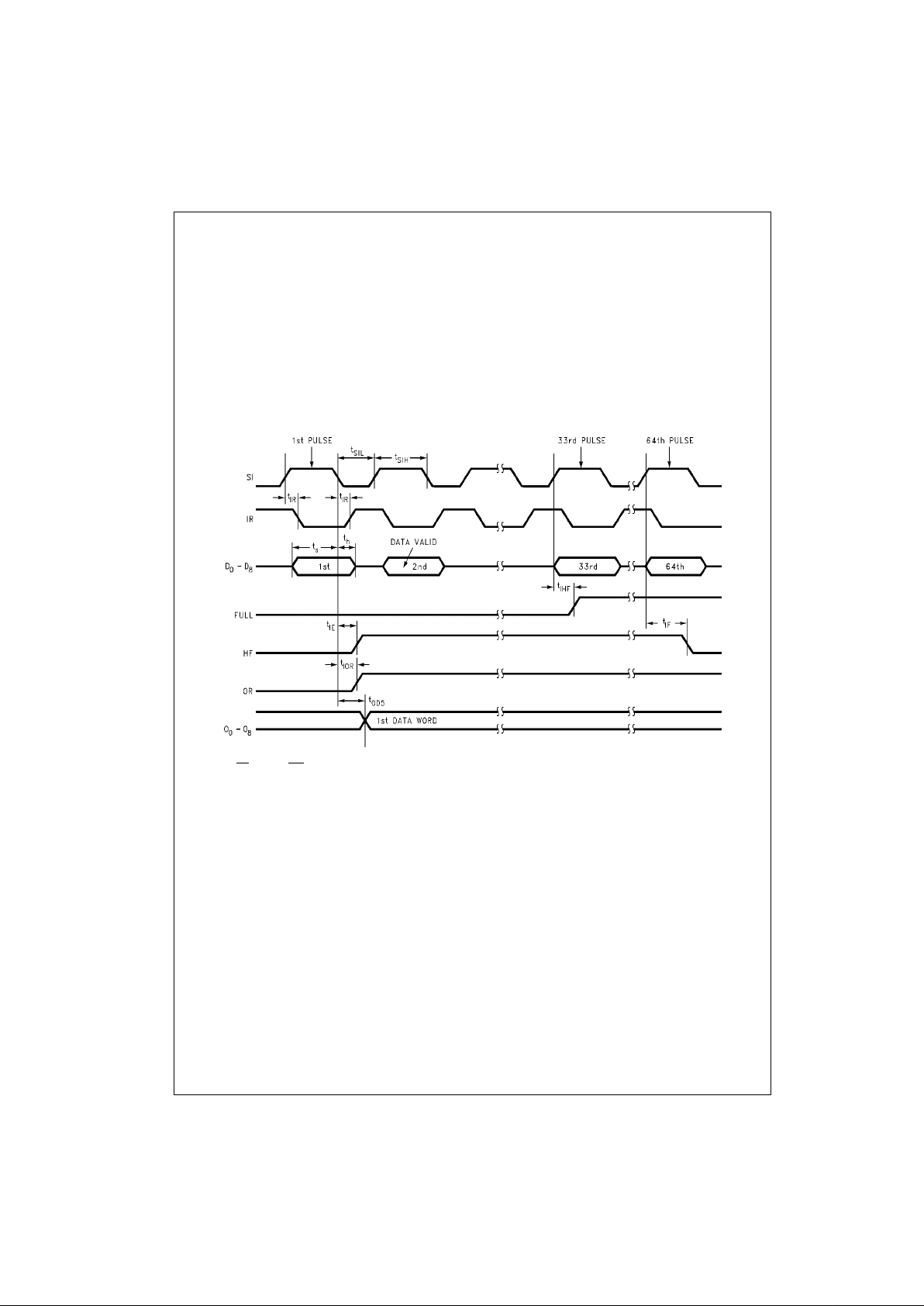
Mode 1: Shift in Sequence for FIFO Empty to Full
Sequence of Operation
1. Input Rea dy is initially HIGH; HF and FULL flags are
LOW. The FIFO is empty and prepared for valid dat a.
OR is LOW indicating that the FIFO is not yet ready to
output data.
2. Sh ift-In is set H IGH, and dat a is loaded in to the FIFO.
Data has to be settled t
s
before the falling edge of SI
and held t
h
after.
3. I nput Read y (IR) goes LOW prop agation delay t
IR
after
SI goes HIGH: input stage is busy.
4. Shift- In is set LOW; IR goes HIGH indicating the FIFO
is ready for additional data. Data just shifted -in arrives
at output propagation delay t
OD5
after SI falls. OR goes
HIGH propagation delay t
IOR
after SI goes LOW, indi-
cating the FIFO has valid data on it s outputs. HF goes
HIGH propagation delay t
IE
after SI falls, indicating the
FIFO is no longer empty.
5. Th e process is repeated thr ough the 64th data word.
On the rising edge of the 33rd SI, FULL flag goes HIGH
propagation delay t
IHF
after SI, indicating a half-full
FIFO. HF goes LOW propagation de lay t
IF
after the ris-
ing edge of the 64th puls e indicating that the FIFO is
full. Any further shift-ins are disabled.
Note: SO and OE are LOW; MR is HIGH.
FIGURE 1. Modes of Operation Mode 1
Page 5

5 www.fairchildsemi.com
74ACT2708
Mode 2: Master Reset
Sequence of Operation
1. Inp ut and Output Ready, HF and FULL can be in any
state before the reset sequence with Master Reset
(MR
) HIGH.
2. Mas ter Reset goes LOW and cle ars the FIFO, setting
up all essential internal states. Master Rese t must be
LOW pulse width t
MRW
before rising again.
3. Master Reset rises.
4. IR r ises ( if not HI GH already) to indica te ready to write
state recovery time t
MRIRH
after the falling edge of MR.
Both HF and FULL will go LOW indicating an empty
FIFO, occurring recovery times t
MRE
and t
MRO
respec-
tively after the falling edge of MR
. OR falls recovery
time t
MRORL
after MR falls. Data at outputs g oes LOW
recovery time t
MRONL
after MR goes LOW.
5. Shift-In can be taken HIGH after a minimum recovery
time t
MRSIH
after MR goes HIGH.
FIGURE 2. Mode of Operation Mode 2
Page 6

www.fairchildsemi.com 6
74ACT2708
Mode 3: With FIFO Full, Shift-In is Held HIGH
in Anticipation of an Empty Location
Sequence of Operation
1. The F IFO is initially full and Shift- In goes HIGH. OR is
initially HIGH. Shift-Out is LOW. IR is LOW.
2. Sh ift-Out is pulsed HIGH, Shift-O ut pulse propagates
and the first data word is lat ched on th e rising edge of
SO. OR falls on this edge. On the falling edg e of SO,
the second data word app ears afte r propag ation delay
t
D
. New data is written into the FIFO after SO goes
LOW.
3. Input Ready goes HIGH one fall-through time, t
FT
, after
the falling edge of SO. Also, HF goes HIGH one t
OF
after SO falls, indicating that the FIFO is no longer full.
4. IR ret urns LOW pulse width t
IP
after rising and shifting
new data in. Also, HF returns LOW pulse width t
3F
after
rising, indicating the FIFO is once more full.
5. Shift-In is brought LOW to complete the shift-in process
and maintain normal operation.
Note: MR and FULL are HIGH; OE is LOW.
FIGURE 3. Modes of Operation Mode 3
Page 7

7 www.fairchildsemi.com
74ACT2708
Mode 4: Shift-Out Sequence, FIFO Full to Empty
Sequence of Operation
1. FIFO is initially full and OR is HIGH, indicating valid
data is at the output. IR is LOW.
2. SO go es HIGH, resulting in OR goi n g LOW one pr opagation delay, t
OR
, after SO rises. OR LOW indicates
output stage is busy.
3. SO goes L OW, new data reaches output on e prop ag ation delay, t
D
, after SO falls; OR goes HIGH one propa-
gation delay, t
OR
, after SO falls and HF rises one
propagation delay, t
OF
, after SO falls. IR rises one fall-
through time, t
FT
, after SO falls.
4. Rep eat process thro ugh the 64th SO pul se. FULL flag
goes LOW one propagation delay, t
OHF
, after the rising
edge of 33rd SO, indicating that the FIFO is less than
half full. On the falling edge of the 64th SO, HF goes
LOW one propagation delay, t
OE
, after SO, indicating
the FIFO is empty. The SO pulse may rise and fall
again with an attempt to unload an empty FIFO. This
results in no change in the data on the outp uts as the
64th word stays latched.
Note: SI and OE are LOW; MR is HIGH; D0–D8 are immaterial.
FIGURE 4. Modes of Operation Mode 4
Page 8

www.fairchildsemi.com 8
74ACT2708
Mode 5: With FIFO Empty, Shift-Out is Held HIGH
in Anticipation of Data
Sequence of Operation
1. FIFO is initially empty; Shift-Out goes HIGH.
2. Sh ift-In p ulse loads d ata into the FIF O and IR falls. HF
rises propagation delay t
X1
after the falling edge of SI.
3. OR rises a fall-through time of t
FTO
after the falling
edge of Shift-In, i ndica ting th at new data is ready t o b e
output.
4. Data arrives at output one propagation delay, t
OD5
,
after the falling edge of Shift-In.
5. OR goes LOW pulse width t
OP
after rising and HF
goes LOW pulse width t
X3
after rising, ind icating that
the FIFO is empty once more.
6. Shi ft-Out goes LOW, necessary to com plete the ShiftOut process.
Note: FULL is LOW; MRis HIGH; OE is LOW; t
DOF
= t
FTO
− t
OD5
. Data output transition—valid data arrives at output stage t
DOF
after OR is HIGH.
FIGURE 5. Modes of Operation Mode 5
Page 9

9 www.fairchildsemi.com
74ACT2708
FIFO Expansion
Word Width Expansion
Word width can be increased by connecting the corr esp ond i ng inp ut con tro l sig nals of mult iple devices. Flags can be m onitored to obtain a composite signal by ANDing the corresponding flags.
Note: AND the corres ponding flags to obtain a composite signal .
FIGURE 6. Word Width Expansion—64 x 18 FIFO
Vmi = 50% VDD for AC/ACQ devices; 1.5V for ACT/ACTQ devices
V
mo
= 50% VDD for AC/ACT, ACQ/ACTQ devices
FIGURE 7. 3-STATE Output Low Enable and
Disable Times for AC/ACT, ACQ/ACTQ
Vmi = 50% VDD for AC/ACQ devices; 1.5V for ACT/ACTQ devices
V
mo
= 50% VDD for AC/ACT, ACQ/ACTQ devi ce s
FIGURE 8. 3-STATE Output High Enable and
Disable Times for AC/ACT, ACQ/ACTQ
Page 10

www.fairchildsemi.com 10
74ACT2708
Absolute Maximum Ratings(Note 1)
Recommended Operating
Conditions
Note 1: Absolute maximum ratings are thos e value s beyond wh ic h dam age
to the device may occur. The databook specif ications should b e met, wit hout exception, to ensure th at the system design is reliable over its power
supply, temperature, and output/inp ut loading variables. Fairchild does no t
recommend operat ion of FACT circuits outside databook specifications.
DC Electrical Characteristics
Note 2: All outputs loaded; thresholds on input associated wit h output under test.
Note 3: Maximum test duration 2.0 ms, one output loaded at a time.
Note 4: Test load 50 pF, 500Ω to ground
Supply Voltage (VCC) −0.5V to +7.0V
DC Input Diode Current (I
IK
)
V
I
= −0.5V −20 mA
V
I
= VCC + 0.5V +20 mA
DC Input Voltage (V
I
) −0.5V to VCC + 0.5V
DC Output Diode Current (I
OK
)
V
O
= −0.5V −20 mA
V
O
= VCC + 0.5V +20 mA
DC Output Voltage (V
O
) −0.5V to VCC + 0.5V
DC Output Source
or Sink Current (I
O
) ±32 mA
DC V
CC
or Ground Current
per Output Pin (I
CC
or I
GND
) ±32 mA
Storage Temperature (T
STG
) −65°C to +150°C
Junction Temperatu r e (T
J
)
PDIP 140°C
Supply Voltage (V
CC
) 4.5V to 5.5V
Input Voltage (V
I
) 0V to V
CC
Output Voltage (VO) 0V to V
CC
Operating Temperature (TA) −40°C to +85°C
Minimum Input Edge Rate (∆V/∆t) 125 mV/ns
V
IN
from 0.8V to 2.0V
V
CC
@ 4.5V, 5.5V
Symbol Parameter
V
CC
TA = 25°CT
A
= −40° to +85°C
Units Conditions
(V) Typ Guaranteed Limits
V
IH
Minimum High Level 4.5 1.5 2.0 2.0 V V
OUT
= 0.1V
Input Voltage 5.5 1.5 2.0 2.0 or VCC −0.1V
V
IL
Maximum Low Level 4.5 1.5 0.8 0.8 V
OUT
= 0.1V
Input Voltage 5.5 1.5 0.8 0.8 or VCC −0.1V
V
OH
Minimum High Level 4.5 4.49 4.4 4.4 V I
OUT
= −50 µA
5.5 5.49 5.4 5.4
VIN = V
IL
or V
IH
4.5 3.86 3.76 V IOH = −8 mA
5.5 4.86 4.76 I
OH
= −8 mA (Note 2)
V
OL
Maximum Low Level 4.5 0.001 0.1 0.1 V I
OUT
= 50 µA
Output Voltage 5.5 0.001 0.1 0.1
VIN = V
IL
or V
IH
4.5 0.36 0.44 V IOL = 8 mA
5.5 0.36 0.44 IOL = 8 mA (Note 2)
I
IN
Maximum Input 5.5 ±0.1 ±1.0 µAVI = VCC, GND
I
OZ
Maximum 5.5 ±0.5 ±5.0 µAVI = VIL, V
IH
3-STATE Current VO = VCC, GND
I
CCT
Maximum ICC/Input 5.5 0.6 1.0 1.5 mA VI = VCC −2.1V
I
OLD
Maximum Dynamic 5.5 32 mA V
OLD
= 1.65V
I
OHD
Output Current (Note 3) 5.5 −32 mA V
OHD
= 3.85V
I
CC
Maximum Quiescent 5.5 8.0 80 µAVIN = V
CC
Supply Current or GND
I
CCD
Supply Current 5.5 125 150 150 mA f = 20 MHz
20 MHz Loaded (Note 4)
Page 11

11 www.fairchildsemi.com
74ACT2708
AC Electrical Characteristics
V
CC
TA = +25°CT
A
= −40°C to +85°C
Symbol Parameter (V)
CL = 50 pF CL = 50 pF
Units
(Note 5) Min Typ Max Min Max
t
PLH
Propagation Delay, t
IR
5.0 2.0 6.5 11.0 1.5 12.5 ns
SI to IR
t
PHL
Propagation Delay, t
IR
5.0 2.0 6.5 11.0 1.5 12.0 ns
SI to IR
t
PLH
Propagation Delay, t
IHF
5.0 4.0 10.5 17.0 4.0 19.5 ns
SI to > HF
t
PHL
Propagation Delay, t
IF
5.0 4.5 10.5 16.5 4.5 19.5 ns
SI to Full Condition
t
PLH
Propagation Delay, t
IE
5.0 4.0 10.0 15.5 4.0 17.5 ns
SI to Not Empty
t
PLH
Propagation Delay, t
IOR
5.0 4.0 13.5 16.5 4.0 19.0 ns
SI to OR
t
PLH
Propagation Delay t
MRIRH
5.0 3.0 8.5 13.5 3.0 15.5 ns
MR to IR
t
PHL
Propagation Delay, t
MRORL
5.0 7.0 16.5 25.5 7.0 29.0 ns
MR to OR
t
PHL
Propagation Delay, t
MRO
5.0 3.5 9.0 14.0 3.5 16.0 ns
MR to Full Flag
t
PHL
Propagation Delay, t
MRE
5.0 8.0 17.5 27.5 8.0 30.5 ns
MR to HF Flag
t
PHL
Propagation Delay, t
MRONL
5.0 3.0 9.0 15.0 3.0 17.0 ns
MR to On, LOW
t
PLH
Propagation Delay, t
D
5.0 6.5 18.5 27.0 6.5 31.0 ns
SO to Data Out
t
PHL
Propagation Delay, t
D
5.0 6.5 18.5 29.5 6.5 34.5 ns
SO to Data Out
t
PHL
Propagation Delay, t
OHF
5.0 3.5 8.5 13.5 3.5 15.5 ns
SO to < HF
t
PLH
Propagation Delay, t
OF
5.0 5.0 12.5 19.5 5.0 22.0 ns
SO to Not Full
t
PLH
, t
PHL
Propagation Delay, t
OR
5.0 2.5 7.0 11.5 2.5 13.5 ns
SO to OR
t
PHL
Propagation Delay, t
OE
5.0 3.5 9.5 15.5 3.0 17.5 ns
SO to Empty
t
PLH
Propagation Delay, t
OD5
5.0 7.0 19.0 30.5 6.0 35.5 ns
SI to New Data Out
t
PHL
Propagation Delay, t
OD5
5.0 7.0 19.0 29.5 6.0 34.5 ns
SI to New Data Out
t
PLH
Propagation Delay, t
X1
5.0 3.5 10.0 16.0 2.5 18.0 ns
SI to HF
t
PLH
Fall-Through Time, t
FTO
5.0 3.5 13.5 21.0 1.5 24.0 ns
SI to OR
t
W
R Pulse Width, t
OP
5.0 12.5 17.0 26.0 12.5 30.5 ns
Page 12

www.fairchildsemi.com 12
74ACT2708
AC Electrical Charac teristics (Continued)
Note 5: Voltage Range 5.0 is 5.0V ± 0.5V
AC Operating Requirements
Note 6: Voltage Range 5.0 is 5.0V ± 0.5V
Capacitance
V
CC
TA = +25°CT
A
= −40°C to +85°C
Symbol Paramete r (V)
CL = 50 pF CL = 50 pF
Units
(Note 5) Min Typ Max Min Max
t
W
HF Pulse Width, t
X3
5.0 14.5 20.5 30.5 14.5 36.5 ns
t
W
IR Pulse Width, t
IP
5.0 16.5 28.0 43.0 16.5 51.5 ns
t
W
HF Pulse Width, t
3F
5.0 17.5 30.0 46.5 17.5 56.0 ns
t
PLH
Fall-Through Times, t
FT
5.0 6.0 15.0 23.5 2.5 28.0 ns
SO to IR
t
PZL
Output Enable 5.0 2.0 6.5 11.0 1.5 12.0 ns
OE to O
n
t
PLZ
Output Disable 5.0 1.5 5.0 8.5 1.5 9.5 ns
OE to O
n
t
PZH
Output Enable 5.0 2.0 7.0 12.0 1.5 13.0 ns
OE to O
n
t
PHZ
Output Disable 5.0 1.5 7.0 12.0 1.5 13.0 ns
OE to O
n
f
SI
Maximum SI 5.0 55 85 45 MHz
Clock Frequency
f
SO
Maximum SO 5.0 42 60 35 MHz
Clock Frequency
V
CC
TA = +25°C T
A
= −40°C to +85°C
Symbol Parameter (V )
CL = 50 pF CL = 50 pF
Units
(Note 6) Typ Guaranteed Minimum
tW(H) SI Pulse Width, t
SIH
5.0 3.5 6.5 7.5 ns
tW(L) SI Pulse Width, t
SIL
5.0 6.0 10.0 12.0 ns
t
S
Setup Time, HIGH or 5.0 1.0 3.5 4.5 ns
LOW, Dn to SI
t
H
Hold Time, HIGH or 5.0 1.5 3.5 4.5 ns
LOW, Dn to SI
t
W
MR Pulse Width, t
MRW
5.0 13.0 20.0 24.5 ns
t
rec
Recovery Time, t
MRSIH
5.0 4.5 7.5 8.5 ns
MR to SI
tW(H) SO Pulse Width, t
SOH
5.0 7.5 6.5 8.0 ns
tW(L) SO Pulse Width, t
SOL
5.0 9.0 14.0 17.0 ns
Symbol Parameter Typ Units Conditions
C
IN
Input Capacitance 4.5 pF VCC = OPEN
C
PD
Power Dissipation Capacitance 20.0 pF VCC = 5.0V
Page 13

Fairchild does not assume any responsibility for use of any circuitry described, no circuit patent licenses are implied and Fairchild reser ves the right at any time without notice to change said circuitry and specifications.
74ACT2708 64 x 9 First-In, First-Out Memory
LIFE SUPPORT POLICY
FAIRCHILD’S PRODUCTS ARE NOT AUTHORIZED FOR USE AS CRITICAL COMPONENTS IN LIFE SUPPORT
DEVICES OR SYSTEMS WITHOUT THE EXPRESS WRITTEN APPROVAL OF THE PRESIDENT OF FAIRCHILD
SEMICONDUCTOR CORPORATION. As used herein:
1. Life support devices or system s a re devices or syste ms
which, (a) are intended for surgical implant into the
body, or (b) support or sustain life, and (c) whose failure
to perform when properly used in accordance with
instructions for use provided in the labeli n g, can be re asonably expected to result i n a significant injur y to the
user.
2. A critical componen t in any com ponen t of a life support
device or system whose failure to perform can be reasonably expected to cause the failure of the life support
device or system, or to affect its safety or effectiveness.
www.fairchildsemi.com
Physical Dimensions inches (millimeters) unless otherwise noted
28-Lead Plastic Dual-In-Line Package (PDIP), JEDEC MS-010, 0.600” Wide
Package Number N28B
 Loading...