

Datasheet 74ACT258SJX, 74ACT258SJ, 74ACT258SCX, 74ACT258SC, 74ACT258PC Datasheet (Fairchild Semiconductor)
...Page 1
© 1999 Fairchild Semiconductor Corporation DS009950 www.fairchildsemi.com
November 1988
Revised November 1999
74ACT258 Quad 2-Input Multiplexer with 3-STATE Outputs
74ACT258
Quad 2-Input Multiplexer with 3-STATE Outputs
General Description
The ACT258 is a quad 2-input multiplexer with 3-STATE
outputs. Four bits of data from two sources can be selected
using a common data select input. The four outputs
present the selected data in the complement (inverted)
form. The outputs may be switc hed to a high impedance
state with a HIGH on the common Output Enable (OE
)
input, allowing the outpu ts to i nt erf ace d irectly with bus-oriented systems.
Features
■ ICC and IOZ reduced by 5 0%
■ Multiplexer expansion by tying outputs together
■ Inverting 3-STATE outputs
■ Outputs source/sink 24 mA
■ TTL-compatible inputs
Ordering Code:
Device also available in Tape and Reel. Specify by appending s uffix let te r “X” to the ordering code.
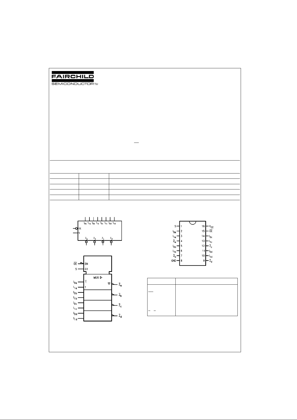
Logic Symbols
IEEE/IEC
Connection Diagram
Pin Descriptions
FACT is a trademark of Fairchild Semiconductor Corporation.
Order Number Package Number Package Description
74ACT258SC M16A 16-Lead Small Outline Integrated Circuit (SOIC), JEDEC MS-012, 0.150” Narrow Body
74ACT258SJ M16D 16-Lead Small Outline Package (SOP), EIAJ TYPE 11, 5.3mm Wide
74ACT258MTC MTC16 16-Lead Thin Shrink Small Outline Package (TSSOP), JEDEC MO-153, 4.4mm Wide
74ACT258PC N16E 16-Lead Plastic Dual-In-Line Package (PDIP), JEDEC MS-001, 0.300” Wide
Pin Names Description
S Common Data Select Input
OE
3-STATE Output Enable Input
I
0a–I0d
Data Inputs from Source 0
I
1a–I1d
Data Inputs from Source 1
Z
a–Zd
3-STATE Inverting Data Outputs
Page 2

www.fairchildsemi.com 2
74ACT258
Truth Table
H = HIGH Voltage Level
L = LOW Voltage Level
X = Immaterial
Z = High Impedance
Functional Description
The ACT258 is a quad 2-in put multiplexer with 3-STATE
outputs. It selects fou r bits o f data from two sour ces und er
control of a common Select input (S). When the Select
input is LOW, the I
0x
inputs are selected an d when Select
is HIGH, the I
1x
inputs are selected. The data on the
selected inputs appe ars at the outputs in inverted for m.
The ACT258 is the logic implementation of a 4-pole, 2position switch where the position of the switch is d etermined by the logi c levels s upplied to the Select inp ut. The
logic equations for the outputs are shown below:
Z
a
= OE • (I1a • S + I0a • S)
Z
b
= OE • (I1b • S + I0b • S)
Z
c
= OE • (I1c • S + I0c • S)
Z
d
= OE • (I1d • S + I0d • S)
When the Output Enable input (OE
) is HIGH, the outputs
are forced to a high imped ance state. If the o utputs of the
3-STATE devices are tied toget her, all but one de vi ce m ust
be in the high impedance st ate to avoid h igh currents that
would exceed the maximum ratings. Designers should
ensure that Output Enable signals to 3-STATE devices
whose outputs are tied together are designed so there is
no overlap.
Logic Diagram
Please note that this diagram is provided only for the understanding of logic operations and should not be used to estimate propagation delays.
Output Select Data
Outputs
Enable Input Inputs
OE
SI0I
1
Z
HXXXZ
LHXLH
LHXHL
Page 3
3 www.fairchildsemi.com
74ACT258
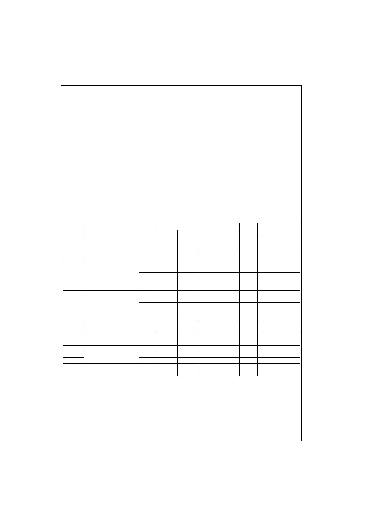
Absolute Maximum Ratings(Note 1) Recommended Operating
Conditions
Note 1: Absolute max imum ratings are those values beyond w hich damage
to the device may occu r. The databook spe cificatio ns shou ld be met, wit hout exception, to ensure that the system de sign is relia ble over its p ower
supply, temperature, and output/input loading variables. Fairchild does not
recommend operation of FACT circuits outside databook specif ic at ions.
DC Electrical Characteristics
Note 2: All outputs loaded; thres holds on input associate d w it h output under test.
Note 3: Maximum test duration 2.0 ms, one output loaded at a time.
Supply Voltage (VCC) −0.5V to +7.0V
DC Input Diode Current (I
IK
)
V
I
= −0.5V −20 mA
V
I
= VCC + 0.5V +20 mA
DC Input Voltage (V
I
) −0.5V to VCC + 0.5V
DC Output Diode Current (I
OK
)
V
O
= −0.5V −20 mA
V
O
= VCC + 0.5V +20 mA
DC Output Voltage (V
O
) −0.5V to VCC + 0.5V
DC Output Source
or Sink Current (I
O
) ±50 mA
DC V
CC
or Ground Current
per Output Pin (I
CC
or I
GND
) ±50 mA
Storage Temperature (T
STG
) −65°C to +150°C
Junction Temperature (T
J
)
PDIP 140°C
Supply Voltage (V
CC
) 4.5V to 5.5V
Input Voltage (V
I
) 0V to V
CC
Output Voltage (VO) 0V to V
CC
Operating Temperature (TA) −40°C to +85°C
Minimum Input Edge Rate (∆V/∆t)
V
IN
from 0.8V to 2.0V
V
CC
@ 4.5V, 5.5V 125 mV/ns
Symbol Parameter
V
CC
TA = +25°CT
A
= −40°C to +85°C
Units Conditions
(V) Typ Guaranteed Limits
V
IH
Minimum HIGH Level 4.5 1.5 2.0 2.0
V
V
OUT
= 0.1V
Input Voltage 5.5 1.5 2.0 2.0 or VCC − 0.1V
V
IL
Maximum LOW Level 4.5 1.5 0.8 0.8
V
V
OUT
= 0.1V
Input Voltage 5.5 1.5 0.8 0.8 or VCC − 0.1V
V
OH
Minimum HIGH Level 4.5 4.49 4.4 4.4
VI
OUT
= −50 µA
Output Voltage 5.5 5.49 5.4 5.4
VIN = VIL or V
IH
4.5 3.86 3.76 V IOH = −24 mA
5.5 4.86 4.76 IOH = −24 mA (Note 2)
V
OL
Maximum LOW Level 4.5 0.001 0.1 0.1
VI
OUT
= 50 µA
Output Voltage 5.5 0.001 0.1 0.1
VIN = VIL or V
IH
4.5 0.36 0.44 V IOL = 24 mA
5.5 0.36 0.44 I
OL
= 24 mA (Note 2)
I
IN
Maximum Input
5.5 ±0.1 ±1.0 µAV
I
= VCC, GND
Leakage Current
I
OZ
Maximum 3- STATE
5.5 ±0.25 ±2.5 µA
VI = VIL, V
IH
Current VO = VCC, GND
I
CCT
Maximum ICC/Input 5.5 0.6 1.5 mA VI = VCC − 2.1V
I
OLD
Minimum Dynamic 5.5 75 mA V
OLD
= 1.65V Max
I
OHD
Output Current (Note3) 5.5 −75 mA V
OHD
= 3.85V Min
I
CC
Maximum Quiescent
5.5 4.0 40.0 µA
VIN = V
CC
Supply Current or GND
Page 4

www.fairchildsemi.com 4
74ACT258
AC Electrical Characteristics
Note 4: Voltage Range 5.0 is 5.0V ± 0.5V
Capacitance
V
CC
TA = +25°CT
A
= −40°C to +85°C
Symbol Parameter (V)
CL = 50 pF CL = 50 pF
Units
(Note 4) Min Typ Max Min Max
t
PLH
Propagation Delay
5.0 2.0 6.5 8.5 1.5 9.5 ns
In to Z
n
t
PHL
Propagation Delay
5.0 2.0 5.5 7.5 1.5 8.0 ns
In to Z
n
t
PLH
Propagation Delay
5.0 3.0 7.5 10.5 2.0 11.5 ns
S to Z
n
t
PHL
Propagation Delay
5.0 1.5 7.0 9.5 1.5 11.0 ns
S to Z
n
t
PZH
Output Enable Time 5.0 2.0 6.5 8.5 1.5 9.5 ns
t
PZL
Output Enable Time 5.0 2.0 6.5 8.5 1.5 9.5 ns
t
PHZ
Output Disable Time 5.0 1.5 7.0 9.0 1.0 10.0 ns
t
PLZ
Output Disable Time 5.0 2.0 6.0 8.0 1.5 9.0 ns
Symbol Parameter Typ Units Conditions
C
IN
Input Capacitance 4.5 pF VCC = OPEN
C
PD
Power Dissipation Capacitance 55.0 pF VCC = 5.0V
Page 5

5 www.fairchildsemi.com
74ACT258
Physical Dimensions inches (millimeters) unless otherwise noted
16-Lead Small Outline Integrated Circuit (SOIC), JEDEC MS-012, 0.150” Narrow Body
Package Number M16A
Page 6

www.fairchildsemi.com 6
74ACT258
Physical Dimensions inches (millimeters) unless otherwise noted (Continued)
16-Lead Small Outline Package (SOP), EIAJ TYPE II, 5.3mm Wide
Package Number M16D
Page 7

7 www.fairchildsemi.com
74ACT258
Physical Dimensions inches (millimeters) unless otherwise noted (Continued)
16-Lead Thin Shrink Sm all Ou tline Pa ck age (TS SO P), JE DE C MO-153, 4.4mm Wide
Package Number MTC16
Page 8

www.fairchildsemi.com 8
74ACT258 Quad 2-Input Multiplexer with 3-STATE Outputs
Physical Dimensions inches (millimeters) unless otherwise noted (Continued)
16-Lead Plastic Dual-In-Line Package (PDIP), JEDEC MS-001, 0.300” Wide
Package Number N16E
Fairchild does not assume any responsibility for use of any circuitr y described, no circuit patent licenses are implied and
Fairchild reserves the right at any time without notice to change said circuitry and specifications.
LIFE SUPPORT POLICY
FAIRCHILD’S PRODUCTS ARE NOT AUTHORIZED FOR USE AS CRITICAL COMPONENTS IN LIFE SUPPORT
DEVICES OR SYSTEMS WITHOUT THE EXPRESS WRITTEN APPROVAL OF THE PRESIDENT OF FAIRCHILD
SEMICONDUCTOR CORPORATION. As used herein:
1. Life support devices or systems are devices or syste ms
which, (a) are intended for surgical implant into the
body, or (b) support or sustain life, and (c) whose failure
to perform when properly used in accordance with
instructions for use provided in the labeling, can be reasonably expected to result in a significant inju ry to the
user.
2. A critical component in any compon ent of a lif e supp ort
device or system whose failure t o perform can be reasonably expected to ca use the failure of the life supp ort
device or system, or to affect its safety or effectiveness.
www.fairchildsemi.com
 Loading...