

Page 1
74ACT257
QUAD 2 CHANNEL MULTIPLEXER (3-STATE)
■ HIGH SPEED: t
■ LOW POWE RDISSIPATION:
=8 µA (MAX.)at TA=25oC
I
CC
■ COMPATIBLEWITHTTL OUTPUTS
V
=2V(MIN),VIL= 0.8V(MAX)
IH
■ 50Ω TRANSMISSIONLINEDRIVING
=5ns(TYP.)at VCC=5V
PD
CAPABILITY
■ SYMMETRICALOUTPUTIMPEDANCE:
|I
|=IOL=24mA(MIN)
OH
■ BALANCEDPROPAGATIONDELAYS:
t
≅ t
PLH
PHL
■ OPERATINGVOLTAGE RANGE:
V
(OPR)= 4.5Vto 5.5V
CC
■ PINAND FUNCTION COMPATIBLE WITH
74 SERIES257
■ IMPROVED LATCH-UP IMMUNITY
DESCRIPTION
The ACT257 is an advanced high-speed CMOS
QUAD 2 CHANNEL MULTIPLEXER (3-STATE)
fabricated with sub-micron silicon gate and
double-layermetal wiring C
2
MOS technology.
It is ideal for low power applications mantaining
high speed operation similar to equivalentBipolar
SchottkyTTL.
These IC’s are composed of an independent 2
channel multiplexer with common SELECT and
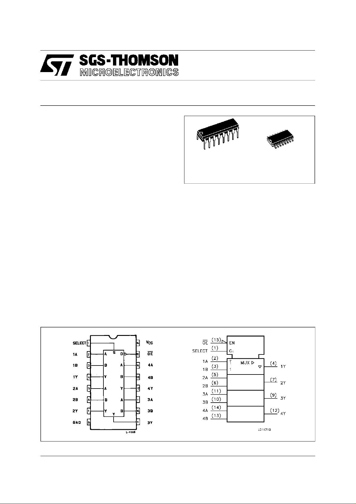
B
(Plastic Package)
(Micro Package)
M
ORDERCODES :
74ACT257B 74ACT257M
ENABLEINPUT.
TheAC257 is a noninverting multiplexer.
When the ENABLE INPUT is held ”High” outputs
of both IC’s become high impedance state. If
SELECT INPUT is held ”Low”, ”A” data is
selected, when SELECT INPUT is ”High”, ”B”
datais closen.
The device is designed to interface directly High
Speed CMOS systems with TTL, NMOS and
CMOSoutput voltage levels.
All inputs and outputs are equipped with
protectioncircuits against static discharge, giving
them 2KV ESD immunity and transient excess
voltage.
PINCONNECTION AND IEC LOGIC SYMBOLS
April 1997
1/10
Page 2
74ACT257
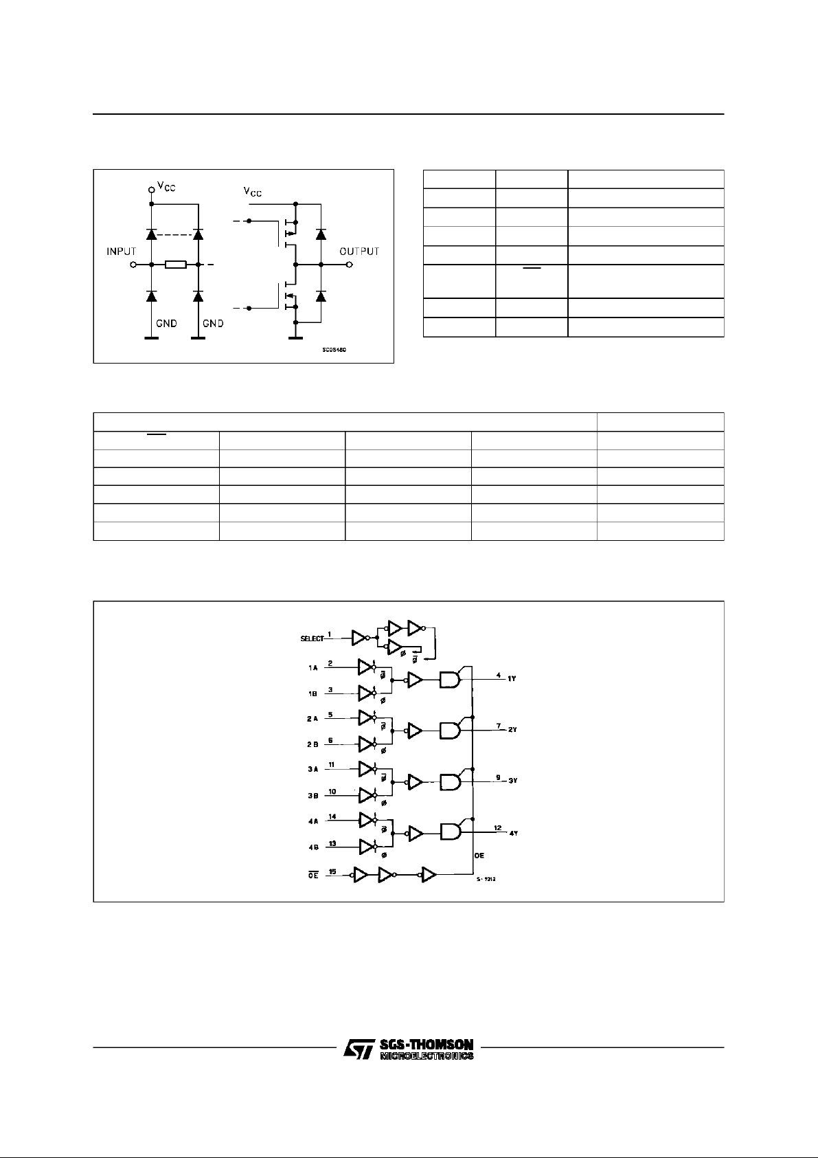
INPUTAND OUTPUTEQUIVALENTCIRCUIT
TRUTH TABLE
INPUTS OUTPUTS
OESELECTABY
HXXXZ
LLLXL
LLHXH
LHXLL
LHXHH
X = DON’T CARE Z =HIGH IMPEDANCE
PIN DESCRIPTION
PI N No SYM B O L NAME A ND FUNCTI ON
1 SELECT Common Data Select Input
2, 5, 14, 11 1A to 4A Data Input From Source A
3, 6, 13, 10 1B to 4B Data Inputs from Source B
4, 7, 12, 9 1Y to 4Y 3 State Multiplexer Outputs
15 OE 3 State Output Enable
Inputs (Active LOW)
8 GND Ground (0V)
16 V
CC
Positive Supply Voltage
LOGICDIAGRAMS
This logic diagram has not be used to estimate propagation delays
2/10
Page 3
74ACT257
ABSOLUTE MAXIMUMRATINGS
Symb o l Parame t er Val u e Uni t
V
V
V
I
I
OK
I
orI
I
CC
T
T
Absolute Maximum Ratings are those values beyond which damage to thedevice may occur. Functional operation under these condition is not implied.
RECOMMENDEDOPERATINGCONDITIONS
Symbol Parameter Valu e Unit
V
V
V
T
dt/dv Input Rise and Fall Time V
1) VINfrom0.8Vto2.0V
Supply Voltage -0.5 to +7 V
CC
DC Input Voltage -0.5 to VCC+ 0.5 V
I
DC Output Voltage -0.5 to VCC+ 0.5 V
O
DC Input Diode Current ± 20 mA
IK
DC Output Diode Current ± 20 mA
DC Output Current ± 50 mA
O
DC VCCor Ground Current ± 200 mA
GND
Storage Temperature -65 to +150
stg
Lead Temperature (10 sec) 300
L
Supply Voltage 4.5 to 5.5 V
CC
Input Voltage 0 to V
I
Output Voltage 0 to V
O
Operating Temperature: -40 to +85
op
= 4.5 to 5.5V (note 1) 8 ns/V
CC
CC
CC
o
C
o
C
V
V
o
C
3/10
Page 4

74ACT257
DC SPECIFICATIONS
Symbol Parameter Test Condition s Value Unit
T
V
CC
(V)
High Level Input Voltage 4.5 VO= 0.1 V or
V
IH
5.5 2.0 1.5 2.0
Low Level Input Voltage 4.5 VO= 0.1 V or
V
IL
5.5 1.5 0.8 0.8
High Level Output
V
OH
Voltage
4.5
5.5 I
4.5 I
5.5 I
Low Level Output
V
OL
Voltage
4.5
5.5 I
4.5 I
5.5 I
Input Leakage Current
I
I
3 State Output Leakage
I
OZ
5.5
5.5 VI=VIHor V
Current
Max ICC/Input 5.5 VI=VCC-2.1 V 0.6 1.5 mA
I
CCT
Quiescent Supply
I
CC
5.5 VI=VCCor GND 8 80 µA
V
- 0.1 V
CC
- 0.1 V
V
CC
IO=-50 µA 4.4 4.49 4.4
(*)
=
V
I
V
IH
V
IL
(*)
V
I
V
IH
V
IL
=-50 µA 5.4 5.49 5.4
O
or
=-24 mA 3.86 3.76
O
=-24 mA 4.86 4.76
O
IO=50 µA 0.001 0.1 0.1
=
=50 mA 0.001 0.1 0.1
O
or
=24 mA 0.36 0.44
O
=24 mA 0.36 0.44
O
VI=VCCor GND ±0.1 ±1 µA
VO=VCCor GND
IL
=25oC-40to85
A
Min. T yp . Max. Min . Max.
2.0 1.5 2.0
1.5 0.8 0.8
±0.5 ±5 µA
o
C
Current
Dynamic Output Current
I
OLD
(note 1, 2)
I
OHD
1) Maximum test duration 2ms, one output loaded at time
2) Incident wave switching is guaranteed on transmission lines with impedances as lowas 50 Ω.
(*)All outputs loaded.
5.5 V
= 1.65 V max 75 mA
OLD
V
= 3.85 V min -75 mA
OHD
V
V
V
V
4/10
Page 5

AC ELECTRICAL CHARACTERISTICS (CL= 50 pF, RL=500 Ω, Input tr=tf=3ns)
74ACT257
Symbol Parameter Test Cond ition Value Unit
o
C
t
Propagation Delay Time
PLH
t
A, B to Y
PHL
Propagation Delay Time
t
PLH
t
SEL to Y
PHL
Output Enable Time 5.0
t
PZL
t
PZH
t
Output Disable Time 5.0
PLZ
t
PHZ
(*) Voltagerangeis5V± 0.5V
V
(V)
5.0
5.0
CC
T
=25oC-40to85
A
Min. T yp . Max. Min . Max.
(*)
(*)
(*)
(*)
5.0 7.0 8.0 ns
6.0 9.0 10.0 ns
5.0 8.0 9.0 ns
6.0 9.0 10.0 ns
CAPACITIVE CHARACTERISTICS
Symbol Parameter Test Condition s Value Unit
T
V
CC
(V)
Input Capacitance
C
IN
C
Input Capacitance
OUT
Power Dissipation
C
PD
5.0
5.0
5.0 31 pF
=25oC-40to85
A
Min. T yp . Max. Min . Max.
4
8
Capacitance (note 1)
1) CPDis defined as the value of the IC’s internal equivalent capacitance which is calculated from the operating current consumption without load. (Refer to
Test Circuit). Average operating current can be obtained by the following equation. I
(opr) = CPD• VCC•fIN+ICC/n (percircuit)
CC
o
C
pF
pF
TEST CIRCUIT
TEST SWITC H
t
PLH,tPHL
t
PZL,tPLZ
t
PZH,tPHZ
CL= 50 pF or equivalent (includes jig and probe capa citance)
= 500Ω or equivalent
R
L=R1
R
of pulse generator (typically 50Ω)
T=ZOUT
Open
2V
CC
Open
5/10
Page 6

74ACT257
WAVEFORM 1: PROPAGATION DELAYS FOR INVERTINGCONDITIONS (f=1MHz;50% duty cycle)
WAVEFORM 2: PROPAGATION DELAYS FOR NON-INVERTING CONDITIONS (f=1MHz; 50% duty
cycle)
6/10
Page 7

WAVEFORM 3: OUTPUTENABLE AND DISABLE TIME (f=1MHz;50% duty cycle)
74ACT257
7/10
Page 8

74ACT257
Plastic DIP16 (0.25)MECHANICAL DATA
DIM.
MIN. TYP. MAX. MIN. TYP. MAX.
a1 0.51 0.020
B 0.77 1.65 0.030 0.065
b 0.5 0.020
b1 0.25 0.010
D 20 0.787
E 8.5 0.335
e 2.54 0.100
e3 17.78 0.700
F 7.1 0.280
I 5.1 0.201
L 3.3 0.130
Z 1.27 0.050
mm inch
8/10
P001C
Page 9

SO16 MECHANICAL DATA
74ACT257
DIM.
MIN. TYP. MAX. MIN. TYP. MAX.
A 1.75 0.068
a1 0.1 0.2 0.004 0.007
a2 1.65 0.064
b 0.35 0.46 0.013 0.018
b1 0.19 0.25 0.007 0.010
C 0.5 0.019
c1 45 (typ.)
D 9.8 10 0.385 0.393
E 5.8 6.2 0.228 0.244
e 1.27 0.050
e3 8.89 0.350
F 3.8 4.0 0.149 0.157
G 4.6 5.3 0.181 0.208
L 0.5 1.27 0.019 0.050
M 0.62 0.024
S 8 (max.)
mm inch
P013H
9/10
Page 10

74ACT257
Information furnished is believed to be accurate and reliable. However, SGS-THOMSONMicroelectronics assumes no responsability for the
consequencesof use of such informationnor for any infringement of patents or otherrights of third parties whichmay results from its use. No
licenseis grantedby implicationor otherwise underany patentor patent rights of SGS-THOMSON Microelectronics.Specificationsmentioned
in this publicationare subject to change without notice.This publication supersedes and replaces all informationpreviously supplied.
SGS-THOMSONMicroelectronics products are notauthorized for useascriticalcomponents in life supportdevices or systems withoutexpress
writtenapproval of SGS-THOMSONMicroelectonics.
1997 SGS-THOMSONMicroelectronics - Printedin Italy - All Rights Reserved
Australia- Brazil - Canada - China- France- Germany- Hong Kong - Italy- Japan- Korea - Malaysia - Malta- Morocco- TheNetherlands -
Singapore- Spain- Sweden - Switzerland- Taiwan - Thailand - United Kingdom - U.S.A
SGS-THOMSONMicroelectronicsGROUPOF COMPANIES
.
10/10
 Loading...