

Datasheet 74AC253CW, 74AC253SJX, 74AC253SJ, 74AC253SCX, 74AC253SC Datasheet (Fairchild Semiconductor)
...Page 1
© 1999 Fairchild Semiconductor Corporation DS009946 www.fairchildsemi.com
November 1988
Revised November 1999
74AC253 • 74ACT253 Dual 4-Input Multiplexer with 3-STATE Outputs
74AC253 • 74ACT253
Dual 4-Input Multiplexer with 3-STATE Outputs
General Description
The AC/ACT253 is a dual 4-input multiplexer with 3-STATE
outputs. It can select two bits of data fr om four sources
using common select inputs. The o utputs may be in dividually switched to a high impedance state with a HIGH on the
respective Output Enable (OE
) inputs, allowing the o utp uts
to interface directly with bus oriented systems.
Features
■ ICC and IOZ reduced by 5 0%
■ Multifunction capability
■ Noninverting 3-STATE outputs
■ Outputs source/sink 24 mA
■ ACT253 has TTL-compatible inputs
Ordering Code:
Device also available Tape and Reel. Specify by appending suffix letter “X” to the ordering code.
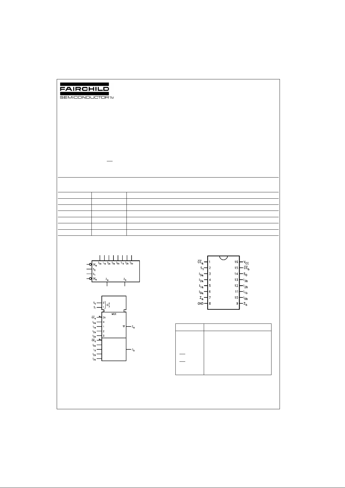
Logic Diagrams
IEEE/IEC
Connection Diagram
Pin Descriptions
FACT is a trademark of Fairchild Semiconductor Corporation.
Order Number Package Number Package Description
74AC253SC M16A 16-Lead Small Outline Integrated Circuit (SOIC), JEDEC MS-012, 0.150” Narrow Body
74AC253SJ M16D 16-Lead Small Outline Package (SOP), EIAJ TYPE II, 5.3mm Wide
74AC253PC N16E 16-Lead Plastic Dual-In-Line Package (PDIP), JEDEC MS-001, 0.300” Wide
74ACT253SC M16A 16-Lead Small Outline Integrated Circuit (SOIC), JEDEC MS-012, 0.150” Narrow Body
74ACT253SJ M16D 16-Lead Small Outline Package (SOP), EIAJ TYPE II, 5.3mm Wide
74ACT253PC N16E 16-Lead Plastic Dual-In-Line Package (PDIP), JEDEC MS-001, 0.300” Wide
Pin Names Description
I
0a–I3a
Side A Data Inputs
I
0b–I3b
Side B Data Inputs
S
0
, S
1
Common Select Inputs
OE
a
Side A Output Enable Input
OE
b
Side B Output Enable Input
Z
a
, Z
b
3-STATE Outputs
Page 2
www.fairchildsemi.com 2
74AC253 • 74ACT253
Functional Description
The AC/ACT253 contains two identical 4-input multiplexers
with 3-STATE outputs. They select two bits from four
sources selected by common Select inputs (S
0
, S1). The 4-
input multiplexers have individual Output Enable (OE
a
,
OE
b
) inputs which, wh en HIGH , fo rce the ou tpu ts to a high
impedance (High Z) st ate. This device is the logi c implementation of a 2-pole, 4-posit ion sw itch, wh ere the positio n
of the switch is determined by the logi c levels supplied to
the two select inpu ts. The logic equations for the outputs
are shown:
Z
a
= OEa • (I0a • S1 • S0 + I1a • S1 • S0 +
I
2a
• S1 • S0 + I3a • S1 • S0)
Z
b
= OEb • (I0b • S1 • S0 + I1b • S1 • S0 +
I
2b
• S1 • S0 + I3b • S1 • S0)
If the outputs of 3- STATE devices are tied together, all but
one device must be in the high impedance state to avoid
high currents that would exceed the maximum ratings.
Designers should ensure that Outp ut Enable signals to 3STATE devices whose outputs are tied together are
designed so that there is no overlap.
Tr uth Table
Address Inputs S0 and S1 are common to both sections.
H = HIGH Voltage Level
L = LOW Voltage Level
X = Immaterial
Z = High Impedance
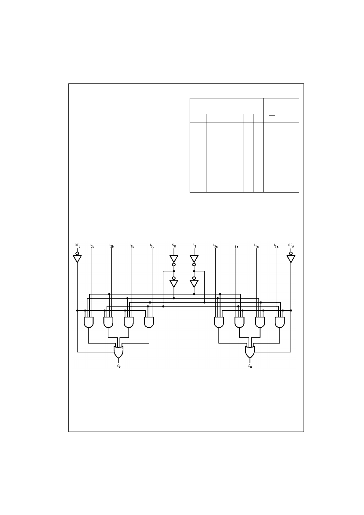
Logic Diagram
Please note that this diagram is provided only for the understanding of logic operations and should not be used to estimate propagation delays.
Select
Data Inputs
Output
Outputs
Inputs Enable
S
0
S1I0I1I2I3OE Z
X X XXXX H Z
L L LXXX L L
L L HXXX L H
HLXLXXL L
HLXHXXL H
LHXXLXL L
LHXXHXL H
HHXXXLL L
HHXXXHL H
Page 3
3 www.fairchildsemi.com
74AC253 • 74ACT253
Absolute Maximum Ratings(Note 1) Recommended Operating
Conditions
Note 1: Absolute max imum ratings are those values beyond w hich damage
to the device may occu r. The databook spe cificatio ns shou ld be met, wit hout exception, to ensure that the system de sign is relia ble over its p ower
supply, temperature, and output/input loading variables. Fairchild does not
recommend operation of FACT circuits outside databook specif ic at ions.
DC Electrical Characteristics for AC
Note 2: All outputs loaded; thres holds on input associate d w it h output under test.
Note 3: Maximum test duration 2.0 ms, one output loaded at a time.
Note 4: I
IN
and ICC @ 3.0V are guaranteed to be less than or equa l t o th e respective limit @ 5.5V VCC.
Supply Voltage (VCC) −0.5V to +7.0V
DC Input Diode Current (I
IK
)
V
I
= −0.5V −20 mA
V
I
= VCC + 0.5V +20 mA
DC Input Voltage (V
I
) −0.5V to VCC + 0.5V
DC Output Diode Current (I
OK
)
V
O
= −0.5V −20 mA
V
O
= VCC + 0.5V +20 mA
DC Output Voltage (V
O
) −0.5V to VCC + 0.5V
DC Output Source
or Sink Current (I
O
) ± 50 mA
DC V
CC
or Ground Current
per Output Pin (I
CC
or I
GND
) ± 50 mA
Storage Temperature (T
STG
) −65°C to +150°C
Junction Temperature (T
J
)
PDIP 140°C
Supply Voltage (V
CC
)
AC 2.0V to 6.0V
ACT 4.5V to 5.5V
Input Voltage (V
I
)0V to V
CC
Output Voltage (VO)0V to V
CC
Operating Temperature (TA) −40°C to +85°C
Minimum Input Edge Rate (∆V/∆t)
AC Devices
V
IN
from 30% to 70% of V
CC
VCC @ 3.3V, 4.5V, 5.5V 125 mV/ns
Minimum Input Edge Rate (∆V/∆t)
ACT Devices
V
IN
from 0.8V to 2.0V
V
CC
@ 4.5V, 5.5V 125 mV/ns
Symbol Parameter
V
CC
(V)
T
A
= +25°CTA = −40°C to +85°C
Units Conditions
Typ Guaranteed Limits
V
IH
Minimum HIGH Level 3.0 1.5 2.1 2.1 V
OUT
= 0.1V
Input Voltage 4.5 2.25 3.15 3.15 V or VCC − 0.1V
5.5 2.75 3.85 3.85
V
IL
Maximum LOW Level 3.0 1.5 0.9 0.9 V
OUT
= 0.1V
Input Voltage 4.5 2.25 1.35 1.35 V or VCC − 0.1V
5.5 2.75 1.65 1.65
V
OH
Minimum HIGH Level 3.0 2.99 2.9 2.9
Output Voltage 4.5 4.49 4.4 4.4 V I
OUT
= −50 µA
5.5 5.49 5.4 5.4
VIN = VIL or V
IH
3.0 2.56 2.46 IOH = −12 mA
4.5 3.86 3.76 V I
OH
= −24 mA
5.5 4.86 4.76 I
OH
= −24 mA (Note 2)
V
OL
Maximum LOW Level 3.0 0.002 0.1 0.1
Output Voltage 4.5 0.001 0.1 0.1 V I
OUT
= 50 µA
5.5 0.001 0.1 0.1
VIN = VIL or V
IH
3.0 0.36 0.44 IOL = 12 mA
4.5 0.36 0.44 V IOL = 24 mA
5.5 0.36 0.44 IOL = 24 mA (Note 2)
IIN (Note 4) Maximum Input Leakage Current 5.5 ± 0.1 ± 1.0 µAVI = VCC, GND
I
OZ
Maximum 3-STATE VI (OE) = VIL, V
IH
Current 5.5 ±0.25 ±2.5 µAVI = VCC, GND
VO = VCC, GND
I
OLD
Minimum Dynamic 5.5 75 mA V
OLD
= 1.65V Max
I
OHD
Output Current (Note 3) 5.5 −75 mA V
OHD
= 3.85V Min
ICC (Note 4) Maximum Quiescent Supply Current 5.5 4.0 40.0 µAVIN = VCC or GND
Page 4

www.fairchildsemi.com 4
74AC253 • 74ACT253
DC Electrical Characteristics for ACT
Note 5: All outputs loaded; thresholds on input assoc iat ed with output under tes t.
Note 6: Maximum test duratio n 2. 0 ms, one output loaded at a time.
AC Electrical Characteristics for AC
Note 7: Voltage Range 3.3 is 3.3V ± 0.3V
Voltage Range 5.0 is 5.0V ± 0.5V
Symbol Parameter
V
CC
TA = +25°CT
A
= −40°C to +85°C
Units Conditions
(V) Typ Guaranteed Limits
V
IH
Minimum HIGH Level 4.5 1.5 2.0 2.0
V
V
OUT
= 0.1V
Input Voltage 5.5 1.5 2.0 2.0 or VCC − 0.1V
V
IL
Maximum L OW Level 4.5 1.5 0.8 0.8
V
V
OUT
= 0.1V
Input Voltage 5.5 1.5 0.8 0.8 or V
CC
− 0.1V
V
OH
Minimum HIGH Level 4.5 4.49 4.4 4.4
VI
OUT
= −50 µA
Output Voltage 5.5 5.49 5.4 5.4
VIN = VIL or V
IH
4.5 3.86 3.76 V IOH = −24 mA
5.5 4.86 4.76 I
OH
= −24 mA (Note 5)
V
OL
Maximum LOW Level 4.5 0.001 0.1 0.1
VI
OUT
= 50 µA
Output Voltage 5.5 0.001 0.1 0.1
VIN = VIL or V
IH
4.5 0.36 0.44 V IOL = 24 mA
5.5 0.36 0.44 IOL = 24 mA (Note 5)
I
IN
Maximum Input
5.5 ±0.1 ±1.0 µAVI = VCC, GND
Leakage Current
I
OZ
Maximum 3-STATE
5.5 ±0.25 ±2.5 µA
VI = VIL, V
IH
Current VO = VCC, GND
I
CCT
Maximum
5.5 0.6 1.5 mA VI = VCC − 2.1V
ICC/Input
I
OLD
Minimum Dynamic 5.5 75 mA V
OLD
= 1.65V Max
I
OHD
Output Current (Note 6) 5.5 −75 mA V
OHD
= 3.85V Min
I
CC
Maximum Quiescent
5.5 4.0 40.0 µA
VIN = V
CC
Supply Current or GND
V
CC
TA = +25°CT
A
= −40°C to +85°C
Symbol Parameter (V)
C
L
= 50 pF CL = 50 pF
Units
(Note 7) Min Typ Max Min Max
t
PLH
Propagation Delay 3.3 2.0 8.5 15.5 2.0 17.5
ns
Sn to Z
n
5.0 2.0 6.5 11.0 1.5 12.5
t
PHL
Propagation Delay 3.3 2.5 9.5 16.0 2.0 18.0
ns
Sn to Z
n
5.0 2.0 7.0 11.5 1.5 13.0
t
PLH
Propagation Delay 3.3 1.5 7.0 14.5 1.5 17.0
ns
In to Z
n
5.0 1.5 5.5 10.0 1.5 11.5
t
PHL
Propagation Delay 3.3 2.0 7.5 13.0 1.5 15.0
ns
In to Z
n
5.0 1.5 5.5 9.5 1.5 11.0
t
PZH
Output Enable Time 3.3 1.5 4.5 8.0 1.0 8.5
ns
5.0 1.5 3.5 6.0 1.0 6.5
t
PZL
Output Enable Time 3.3 1.5 5.0 8.0 1.0 9.0
ns
5.0 1.5 3.5 6.0 1.0 7.0
t
PHZ
Output Disable Time 3.3 2.0 5.5 9.5 1.5 10.0
ns
5.0 2.0 5.0 8.0 1.5 8.5
t
PLZ
Output Disable Time 3.3 1.5 5.0 8.0 1.0 9.0
ns
5.0 1.5 4.0 7.0 1.0 7.5
Page 5

5 www.fairchildsemi.com
74AC253 • 74ACT253
AC Electrical Characteristics for ACT
Note 8: Voltage Range 5.0 is 5.0V ± 0.5V
Capacitance
V
CC
TA = +25°CT
A
= −40°C to +85°C
Symbol Parameter (V)
C
L
= 50 pF CL = 50 pF
Units
(Note 8) Min Typ Max Min Max
t
PLH
Propagation Delay
5.0 2.0 7.0 11.5 2.0 13.0 ns
S
n
to Z
n
t
PHL
Propagation Delay
5.0 3.0 7.5 13.0 2.5 14.5 ns
S
n
to Z
n
t
PLH
Propagation Delay
5.0 2.5 5.5 10.0 2.0 11.0 ns
In to Z
n
t
PHL
Propagation Delay
5.0 3.5 6.5 11.0 3.0 12.5 ns
I
n
to Z
n
t
PZH
Output Enable Time 5.0 2.0 4.5 7.5 1.5 8.5 ns
t
PZL
Output Enable Time 5.0 2.0 5.0 8.0 1.5 9.0 ns
t
PHZ
Output Disable Time 5.0 3.0 6.0 9.5 2.5 10.0 ns
t
PLZ
Output Disable Time 5.0 2.5 4.5 7.5 2.0 8.5 ns
Symbol Parameter Typ Units Conditions
C
IN
Input Capacitance 4.5 pF VCC = OPEN
C
PD
Power Dissipation Capacitance 50.0 pF VCC = 5.0V
Page 6

www.fairchildsemi.com 6
74AC253 • 74ACT253
Physical Dimensions inches (millimeters) unless otherwise noted
16-Lead Small Outline Integrated Circuit (SOIC), JEDEC MS-012, 0.150” Narrow Body
Package Number M16A
Page 7

7 www.fairchildsemi.com
74AC253 • 74ACT253
Physical Dimensions inches (millimeters) unless otherwise noted (Continued)
16-Lead Small Outline Package (SOP), EIAJ TYPE II, 5.3mm Wide
Package Number M16D
Page 8

www.fairchildsemi.com 8
74AC253 • 74ACT253 Dual 4-Input Multiplexer with 3-STATE Outputs
Physical Dimensions inches (millimeters) unless otherwise noted (Continued)
16-Lead Plastic Dual-In-Line Package (PDIP), JEDEC MS-001, 0.300” Wide
Package Number N16E
Fairchild does not assume any responsibility for use of any circuitr y described, no circuit patent licenses are implied and
Fairchild reserves the right at any time without notice to change said circuitry and specifications.
LIFE SUPPORT POLICY
FAIRCHILD’S PRODUCTS ARE NOT AUTHORIZED FOR USE AS CRITICAL COMPONENTS IN LIFE SUPPORT
DEVICES OR SYSTEMS WITHOUT THE EXPRESS WRITTEN APPROVAL OF THE PRESIDENT OF FAIRCHILD
SEMICONDUCTOR CORPORATION. As used herein:
1. Life support devices or systems are devices or syste ms
which, (a) are intended for surgical implant into the
body, or (b) support or sustain life, and (c) whose failure
to perform when properly used in accordance with
instructions for use provided in the labeling, can be reasonably expected to result in a significant inju ry to the
user.
2. A critical component in any compon ent of a lif e supp ort
device or system whose failure t o perform can be reasonably expected to ca use the failure of the life supp ort
device or system, or to affect its safety or effectiveness.
www.fairchildsemi.com
 Loading...