

Datasheet 74AC251SJX, 74AC251SJ, 74AC251SCX, 74AC251SC, 74AC251PC Datasheet (Fairchild Semiconductor)
...Page 1
© 1999 Fairchild Semiconductor Corporation DS009945 www.fairchildsemi.com
November 1988
Revised November 1999
74AC251 • 74ACT251 8-Input Multiplexer with 3-STATE Output
74AC251 • 74ACT251
8-Input Multiplexer with 3-STATE Output
General Description
The AC/ACT251 is a high -speed 8-input digital mu l tipl ex er.
It provides, in one package, the ability to select on e bit of
data from up to eight sources. It can be used as universal
function generator t o generate any logic function of fo ur
variables. Both true and co mplementary outputs are provided.
Features
■ ICC reduced by 50%
■ Multifunctional capability
■ On-chip select logic decoding
■ Inverting and noninverting 3-STATE outputs
■ Outputs source/sink 24 mA
■ ACT251 has TTL-compatible inputs
Ordering Code:
Device also available in Tape and Reel. Specify by appending su ffix le tter “X” to the ordering code.
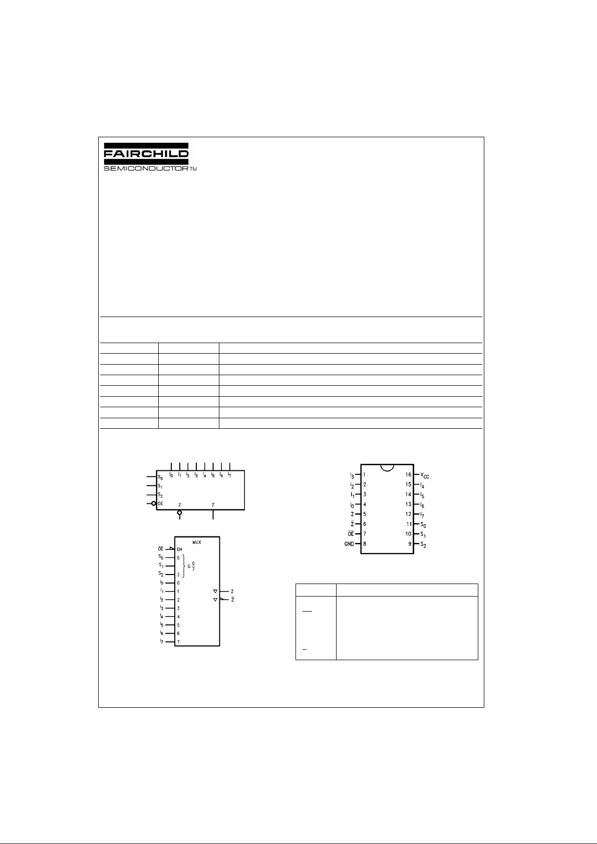
Logic Symbols
IEEE/IEC
Connection Diagram
Pin Descriptions
FACT is a trademark of Fairchild Semiconductor Corporation.
Order Number Package Number Package Description
74AC251SC M16A 16-Lead Small Outline Integrated Circuit (SOIC), JEDEC MS-012, 0.150” Narrow Body
74AC251SJ M16D 16-Lead Small Outline Package (SOP), EIAJ TYPE II, 5.3mm Wide
74AC251MTC MTC16 16-Lead Thin Shrink Small Outline Package (TSSOP), JEDEC MO-153, 4.4mm Wide
74AC251PC N16E 16-Lead Plastic Dual-In-Line Package (PDIP), JEDEC MS-001, 0.300” Wide
74ACT251SC M16A 16-Lead Small Outline Integrated Circuit (SOIC), JEDEC MS-012, 0.150” Narrow Body
74ACT251MTC MTC16 16-Lead Thin Shrink Small Outline Package (TSSOP), JEDEC MO-153, 4.4mm Wide
74ACT251PC N16E 16-Lead Plastic Dual-In-Line Package (PDIP), JEDEC MS-001, 0.300” Wide
Pin Names Description
S
0–S2
Select Inputs
OE
3-STATE Output Enable Input
I
0–I7
Multiplexer Inputs
Z 3-STATE Multiplexer Output
Z
Complementary 3-STATE Multiplexer Output
Page 2
www.fairchildsemi.com 2
74AC251 • 74ACT251
Functional Description
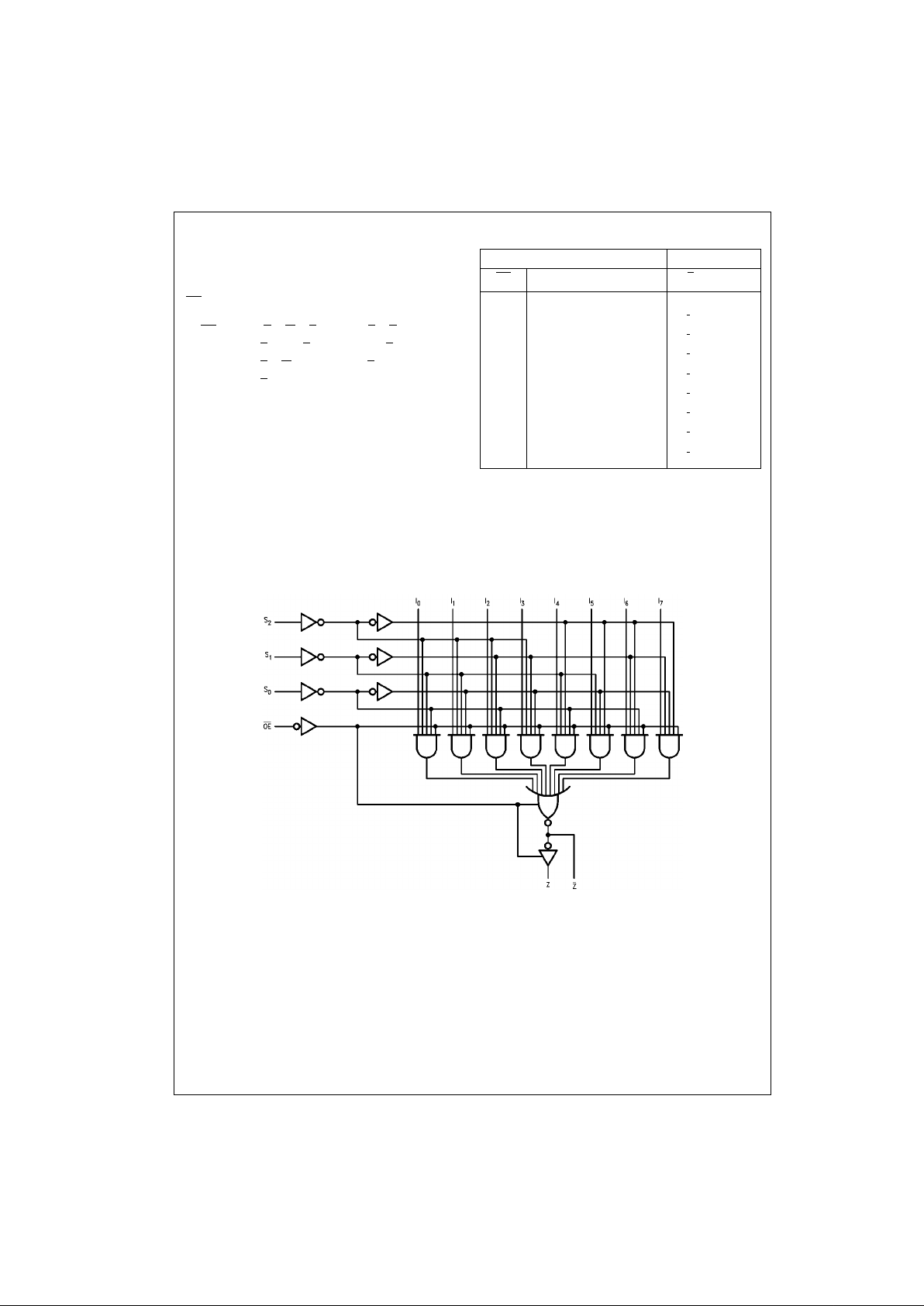
This device is a l ogical i mplementa tion of a sin gle-pol e, 8position switch with the switch position controlled by the
state of three Select i npu ts, S
0
, S1, S2. Both true and com-
plementary outputs ar e provided. The Output Enab le input
(OE
) is active LOW. When it is activated, the logic functio n
provided at the output is:
Z = OE
• (I0 • S0 • S1 • S2 + I1• S0 • S1 • S2 +
I
2
• S0 • S1 • S2 + I3 • S0 • S1 • S2 +
I
4
• S0 • S1 • S2 + I5 • S0 • S1 • S2 +
I
6
• S0 • S1 • S2 + I7 • S0 • S1 • S2)
When the Output Ena ble is HIGH, both outpu ts are in the
high impedance (High Z) state. This feature allows multiplexer expansion by tyi ng the outpu ts of up to 128 dev ices
together. When the outputs of the 3-STATE devices are
tied together, all but one device must b e i n th e h igh im ped ance state to avoi d high currents that would exceed the
maximum ratings. The Output Enable signals should be
designed to ensure there is no overlap in the active-LOW
portion of the enable voltages.
Tr uth Table
H = HIGH Voltage Level
L = LOW Voltage Level
X = Immaterial
Z = High Impedance
Logic Diagram
Please note that this diagram is provided only for the understanding of logic operations and should not be used to estimate propagation delays.
Inputs Outputs
OE S
2
S
1
S
0
Z Z
H X X X Z Z
L L L LI
0
I
0
L L L HI1 I
1
L L H LI2 I
2
L L H HI3 I
3
L H L LI4 I
4
L H L HI5 I
5
L H H LI6 I
6
L H H HI7 I
7
Page 3
3 www.fairchildsemi.com
74AC251 • 74ACT251
Absolute Maximum Ratings(Note 1) Recommended Operating
Conditions
Note 1: Absolute max imum ratings are those values beyond w hich damage
to the device may occu r. The databook spe cificatio ns shou ld be met, wit hout exception, to ensure that the system de sign is relia ble over its p ower
supply, temperature, and output/input loading variables. Fairchild does not
recommend operation of FACT circuits outside databook specif ic at ions.
DC Electrical Characteristics for AC
Note 2: All outputs loaded; thres holds on input associate d w it h output under test.
Note 3: Maximum test duration 2.0 ms, one output loaded at a time.
Note 4: I
IN
and ICC @ 3.0V are guaranteed to be less than or equa l t o th e respective limit @ 5.5V VCC.
Supply Voltage (VCC) −0.5V to +7.0V
DC Input Diode Current (I
IK
)
V
I
= −0.5V −20 mA
V
I
= VCC + 0.5V +20 mA
DC Input Voltage (V
I
) −0.5V to VCC + 0.5V
DC Output Diode Current (I
OK
)
V
O
= −0.5V −20 mA
V
O
= VCC + 0.5V +20 mA
DC Output Voltage (V
O
) −0.5V to VCC + 0.5V
DC Output Source
or Sink Current (I
O
) ±50 mA
DC V
CC
or Ground Current
per Output Pin (I
CC
or I
GND
) ±50 mA
Storage Temperature (T
STG
) −65°C to +150°C
Junction Temperature (T
J
)
PDIP 140°C
Supply Voltage (V
CC
)
AC 2.0V to 6.0V
ACT 4.5V to 5.5V
Input Voltage (V
I
) 0V to V
CC
Output Voltage (VO) 0V to V
CC
Operating Temperature (TA) −40°C to +85°C
Minimum Input Edge Rate (∆V/∆t)
AC Devices
V
IN
from 30% to 70% of V
CC
VCC @ 3.3V, 4.5V, 5.5V 125 mV/ns
Minimum Input Edge Rate (∆V/∆t)
ACT Devices
V
IN
from 0.8V to 2.0V
V
CC
@ 4.5V, 5.5V 125 mV/ns
Symbol Parameter
V
CC
(V)
T
A
= +25°C TA = −40°C to +85°C
Units Conditions
Typ Guaranteed Limits
V
IH
Minimum HIGH Level 3.0 1.5 2.1 2.1 V
OUT
= 0.1V
Input Voltage 4.5 2.25 3.15 3.15 V or VCC − 0.1V
5.5 2.75 3.85 3.85
V
IL
Maximum LOW Level 3.0 1.5 0.9 0.9 V
OUT
= 0.1V
Input Voltage 4.5 2.25 1.35 1.35 V or VCC − 0.1V
5.5 2.75 1.65 1.65
V
OH
Minimum HIGH Level 3.0 2.99 2.9 2.9
Output Voltage 4.5 4.49 4.4 4.4 V I
OUT
= −50 µA
5.5 5.49 5.4 5.4
VIN = VIL or V
IH
3.0 2.56 2.46 IOH = −12 mA
4.5 3.86 3.76 V I
OH
= −24 mA
5.5 4.86 4.76 I
OH
= −24 mA (Note 2)
V
OL
Maximum LOW Level 3.0 0.002 0.1 0.1
Output Voltage 4.5 0.001 0.1 0.1 V I
OUT
= 50 µA
5.5 0.001 0.1 0.1
VIN = VIL or V
IH
3.0 0.36 0.44 IOL = 12 mA
4.5 0.36 0.44 V IOL = 24 mA
5.5 0.36 0.44 IOL = 24 mA (Note 2)
IIN (Note 4) Maximum Input Leakage Current 5.5 ±0.1 ±1.0 µAVI = VCC, GND
I
OZ
Maximum 3-STATE VI (OE) = VIL, V
IH
Current 5.5 ±0.25 ±2.5 µAVI = VCC, V
GND
VO = VCC, GND
I
OLD
Minimum Dynamic 5.5 75 mA V
OLD
= 1.65V Max
I
OHD
Output Current (Note 3) 5.5 −75 mA V
OHD
= 3.85V Min
I
CC
(Note 4) Maximum Quiescent Supply Curent 5.5 4.0 40.0 µAVIN = VCC or GND
Page 4

www.fairchildsemi.com 4
74AC251 • 74ACT251
DC Electrical Characteristics for ACT
Note 5: All outputs loaded; thresholds on input assoc iat ed with output under tes t.
Note 6: Maximum test duratio n 2. 0 ms, one output loaded at a time.
AC Electrical Characteristics for AC
Note 7: Voltage Range 3.3 is 3.3V ± 0.3V.
Voltage Range 5.0 is 5.0V ± 0.5V
Symbol Parameter
V
CC
(V)
T
A
= +25°C TA = −40°C to +85°C
Units Conditions
Typ Guaranteed Limits
V
IH
Minimum HIGH Level 4.5 1.5 2.0 2. 0
V
V
OUT
= 0.1V
Input Voltage 5.5 1.5 2.0 2.0 or VCC − 0.1V
V
IL
Maximum LOW Level 4. 5 1.5 0.8 0.8
V
V
OUT
= 0.1V
Input Voltage 5.5 1.5 0.8 0.8 or V
CC
− 0.1V
V
OH
Minimum HIGH Level 4.5 4.49 4.4 4.4
VI
OUT
= −50 µA
Output Voltage 5.5 5.49 5.4 5.4
VIN = VIL or V
IH
4.5 3.86 3.76 V IOH = −24 mA
5.5 4.86 4.76 I
OH
= −24 mA (Note 5)
V
OL
Maximum LOW Level 4.5 0.001 0.1 0.1
VI
OUT
= 50 µA
Output Voltage 5.5 0.001 0.1 0.1
VIN = VIL or V
IH
4.5 0.36 0.44 V IOL = 24 mA
5.5 0.36 0.44 IOL = 24 mA (Note 5)
I
IN
Maximum Input
5.5 ±0.1 ±1.0 µAVI = VCC, GND
Leakage Current
I
OZ
Maximum 3-STATE
5.5 ±0.5 ±5.0 µA
VI = VIL, V
IH
Current VO = VCC, GND
I
CCT
Maximum
5.5 0.6 1.5 mA VI = VCC − 2.1V
ICC/Input
I
OLD
Minimum Dynamic 5.5 75 mA V
OLD
= 1.65V Max
I
OHD
Output Current (Note6) 5.5 −75 mA V
OHD
= 3.85V Min
I
CC
Maximum Quiescent
5.5 4.0 40.0 µA
VIN = V
CC
Supply Current or GND
V
CC
TA = +25°CT
A
= −40°C to +85°C
Symbol Par am e ter (V)
C
L
= 50 pF CL = 50 pF
Units
(Note 7) Min Typ Max Min Max
t
PLH
Propagation Delay 3.3 1.5 11.5 17.5 1.5 19.0
ns
Sn to Z or Z 5.0 1.5 8.5 12.5 1.5 13.5
t
PHL
Propagation Delay 3.3 1.5 11.0 17.5 1.5 19.0
ns
Sn to Z or Z 5.0 1.5 8.0 12.5 1.5 13.5
t
PLH
Propagation Delay 3.3 1.5 10.0 14.0 1.5 15.5
ns
In to Z or Z 5.0 1.5 7.0 10.0 1.5 11.0
t
PHL
Propagation Delay 3.3 1.5 9.0 14.0 1.5 15.5
ns
In to Z or Z 5.0 1.5 6.5 10.0 1.5 11.0
t
PZH
Output Enable Time 3.3 1.5 7.5 11.0 1.5 12.0
ns
OE to Z or Z 5.0 1.5 5.5 8.0 1.5 9.0
t
PZL
Output Enable Time 3.3 1.5 7.5 11.0 1.5 12.0
ns
OE to Z or Z 5.0 1.5 5.5 8.0 1.5 9.0
t
PHZ
Output Disable Time 3.3 1.5 8.5 11.5 1.5 13.0
ns
OE to Z or Z 5.0 1.5 7.0 9.5 1.5 10.0
t
PLZ
Output Disable Time 3.3 1.5 7.0 11.0 1.5 12.0
ns
OE to Z or Z 5.0 1.5 5.5 8.0 1.5 8.5
Page 5

5 www.fairchildsemi.com
74AC251 • 74ACT251
AC Electrical Characteristics for ACT
Note 8: Voltage Range 5.0 is 5.0V ±0.5V
Capacitance
V
CC
TA = +25°CT
A
= −40°C to +85°C
Symbol Parameter (V)
C
L
= 50 pF CL = 50 pF
Units
(Note 8) Min Typ Max Min Max
t
PLH
Propagation Delay
5.0 2.5 7.0 15.5 2.0 17.0 ns
S
n
to Z or Z
t
PHL
Propagation Delay
5.0 2.5 7.5 16.5 2.5 18.5 ns
S
n
to Z or Z
t
PLH
Propagation Delay
5.0 2.5 5.5 12.0 2.0 13.0 ns
In to Z or Z
t
PHL
Propagation Delay
5.0 2.5 6.5 12.5 2.5 14.0 ns
I
n
to Z or Z
t
PZH
Output Enable Time
5.0 1.5 5.0 8.5 1.5 9.0 ns
OE
to Z or Z
t
PZL
Output Enable Time
5.0 1.5 4.5 8.5 1.5 9.5 ns
OE to Z or Z
t
PHZ
Output Disable Time
5.0 2.0 6.0 12.0 2.0 13.0 ns
OE
to Z or Z
t
PLZ
Output Disable Time
5.0 1.5 4.5 8.5 1.5 9.0 ns
OE
to Z or Z
Symbol Parameter Typ Units Conditions
C
IN
Input Capacitance 4.5 pF VCC = OPEN
C
PD
Power Dissipation Capacitance 70.0 pF VCC = 5.0V
Page 6

www.fairchildsemi.com 6
74AC251 • 74ACT251
Physical Dimensions inches (millimeters) unless otherwise noted
16-Lead Small Outline Integrated Circuit (SOIC), JEDEC MS-012, 0.150” Narrow Body
Package Number M16A
Page 7

7 www.fairchildsemi.com
74AC251 • 74ACT251
Physical Dimensions inches (millimeters) unless otherwise noted (Continued)
16-Lead Small Outline Package (SOP), EIAJ Type II, 5.3mm Wide
Package Number M16D
Page 8

www.fairchildsemi.com 8
74AC251 • 74ACT251
Physical Dimensions inches (millimeters) unless otherwise noted (Continued)
16-Lead Thin Shrink Small Outline Packge (TSSOP), JEDEC MO-153, 4.4mm Wide
Package Number MTC16
Page 9

9 www.fairchildsemi.com
74AC251 • 74ACT251 8-Input Multiplexer with 3-STATE Output
Physical Dimensions inches (millimeters) unless otherwise noted (Continued)
16-Lead Plastic Dual-In-Line Package (PDIP), JEDEC MS-001, 0.3 00” Wide
Package Number N16E
Fairchild does not assume any responsibility for use of any circuitry described , no circuit patent licenses are implied and
Fairchild reserves the right at any time without notice to change said circuitry and specifications.
LIFE SUPPORT POLICY
FAIRCHILD’S PRODUCTS ARE NOT AUTHORIZED FOR USE AS CRITICAL COMPONENTS IN LIFE SUPPORT
DEVICES OR SYSTEMS WITHOUT THE EXPRESS WRITTEN APPROVAL OF THE PRESIDENT OF FAIRCHILD
SEMICONDUCTOR CORPORATION. As used herein:
1. Life support devices or systems are dev ic es or syste ms
which, (a) are intended for surgical implant into the
body, or (b) support or sustain life, and (c) whose failure
to perform when properly used in accordance with
instructions for use provide d in the labe l ing, can be re asonably expected to result in a significant injury to the
user.
2. A critical compo nent in any com ponen t of a life s upp ort
device or system whose failure to perform can be reasonably expected to cause the failure of the l ife support
device or system, or to affect its safety or effectiveness.
www.fairchildsemi.com
 Loading...