

Datasheet 74AC245SJX, 74AC245SJ, 74AC245SCX, 74AC245SC, 74AC245PC Datasheet (Fairchild Semiconductor)
...Page 1
© 1999 Fairchild Semiconductor Corporation DS009944 www.fairchildsemi.com
November 1988
Revised November 1999
74AC245 • 74ACT245 Octal Bidirectional Transceiver with 3-STATE
74AC245 • 74ACT245
Octal Bidirectional Transceiver with 3-STATE
Inputs/Outputs
General Description
The AC/ACT245 contai ns eight non-inverting bidirectional
buffers with 3-STATE outputs and is intended for bu s-oriented applications. Current sinking capability is 24 mA at
both the A and B p orts. The Transmit/Receive (T/R
) input
determines the directi on of data flow through the b idirectional transceiver. Transmit (active-HIGH) enables data
from A ports to B ports; Receive (active-LOW) enables
data from B ports to A ports. The Output Enable input,
when HIGH, disables both A and B ports by placing them in
a HIGH Z condition.
Features
■ ICC and IOZ reduced by 5 0%
■ Noninverting buffers
■ Bidirectional data path
■ A and B outputs source/sink 24 mA
■ ACT245 has TTL-compatible inputs
Ordering Code:
Device also available in Tape and Reel. Specify by appending su ffix le tter “X” to the ordering code.
FACT is a trademark of Fairchild Semiconductor Corporation.
Order Number Package Number Package Description
74AC245SC M20B 20-Lead Small Outline Integrated Circuit (SOIC), JEDEC MS-013, 0.300” Wide Body
74AC245SJ M20D 20-Lead Small Outline Package (SOP), EIAJ TYPE II, 5.3mm Wide
74AC245MTC MTC20 20-Lead Thin Shrink Small Outline Package (TSSOP), JEDEC MO-153, 4.4mm Wide
74AC245PC N20A 20-Lead Plastic Dual-In-Line Package (PDIP), JEDEC MS-001, 0.300” Wide
74ACT245SC M20B 20-Lead Small Outline Integrated Circuit (SOIC), JEDEC MS-013, 0.300” Wide Body
74ACT245SJ M20D 20-Lead Small Outline Package (SOP), EIAJ TYPE II, 5.3mm Wide
74ACT245MSA MSA20 20-Lead Shrink Small Outline Package (SSOP), EIAJ TYPE II, 5.3mm Wide
74ACT245MTC MTC20 20-Lead Thin Shrink Small Outline Package (TSSOP), JEDEC MO-153, 4.4mm Wide
74ACT245PC N20A 20-Lead Plastic Dual-In-Line Package (PDIP), JEDEC MS-001, 0.300” Wide
Page 2
www.fairchildsemi.com 2
74AC245 • 74ACT245
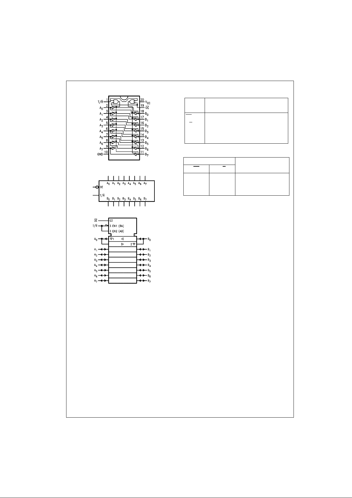
Connection Diagram
Logic Symbols
IEEE/IEC
Pin Descriptions
Tr uth Table
H = HIGH Voltage Level
L = LOW Voltage Level
X = Immaterial
Pin
Description
Names
OE
Output Enable Input
T/R
Transmit/Receive Input
A
0–A7
Side A 3-STATE Inputs or 3-STATE Outputs
B
0–B7
Side B 3-STATE Inputs or 3-STATE Outputs
Inputs
Outputs
OE
T/R
L L Bus B Data to Bus A
L H Bus A Data to Bus B
HXHIGH-Z State
Page 3
3 www.fairchildsemi.com
74AC245 • 74ACT245
Absolute Maximum Ratings(Note 1) Recommended Operating
Conditions
Note 1: Absolute max imum ratings are those values beyond w hich damage
to the device may occu r. The databook spe cificatio ns shou ld be met, wit hout exception, to ensure that the system de sign is relia ble over its p ower
supply, temperature, and output/input loading variables. Fairchild does not
recommend operation of FACT circuits outside databook specif ic at ions.
DC Electrical Characteristics for AC
Note 2: All outputs loaded; thres holds on input associate d w it h output under test.
Note 3: Maximum test duration 2.0 ms, one output loaded at a time.
Note 4: I
IN
and ICC @ 3.0V are guaranteed to be less than or equa l t o th e respective limit @ 5.5V VCC.
Supply Voltage (VCC) −0.5V to +7.0V
DC Input Diode Current (I
IK
)
V
I
= −0.5V −20 mA
V
I
= VCC + 0.5V +20 mA
DC Input Voltage (V
I
) −0.5V to VCC + 0.5V
DC Output Diode Current (I
OK
)
V
O
= −0.5V −20 mA
V
O
= VCC + 0.5V +20 mA
DC Output Voltage (V
O
) −0.5V to VCC + 0.5V
DC Output Source
or Sink Current (I
O
) ±50 mA
DC V
CC
or Ground Current
per Output Pin (I
CC
or I
GND
) ±50 mA
Storage Temperature (T
STG
) −65°C to +150°C
Junction Temperature (T
J
)
PDIP 140°C
Supply Voltage (V
CC
)
AC 2.0V to 6.0V
ACT 4.5V to 5.5V
Input Voltage (V
I
)0V to V
CC
Output Voltage (VO)0V to V
CC
Operating Temperature (TA) −40°C to +85°C
Minimum Input Edge Rate (∆V/∆t)
AC Devices
V
IN
from 30% to 70% of V
CC
VCC @ 3.3V, 4.5V, 5.5V 125 mV/ns
Minimum Input Edge Rate (∆V/∆t)
ACT Devices
V
IN
from 0.8V to 2.0V
V
CC
@ 4.5V, 5.5V 125 mV/ns
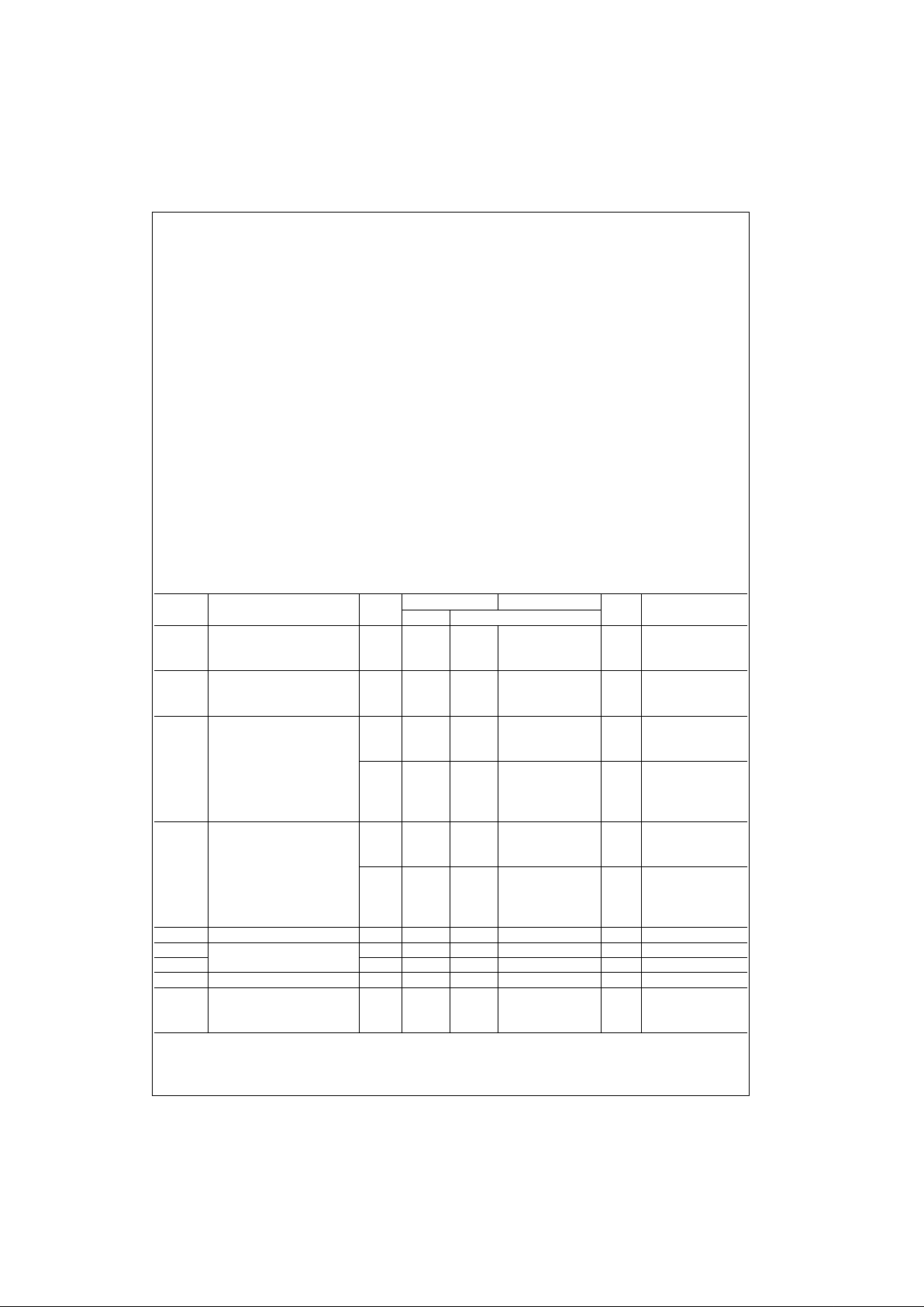
Symbol Parameter
V
CC
(V)
T
A
= +25°CTA = −40°C to +85°C
Units Conditions
Typ Guaranteed Limits
V
IH
Minimum HIGH Level 3.0 1.5 2.1 2.1 V
OUT
= 0.1V
Input Voltage 4.5 2.25 3.15 3.15 V or VCC − 0.1V
5.5 2.75 3.85 3.85
V
IL
Maximum LOW Level 3.0 1.5 0.9 0.9 V
OUT
= 0.1V
Input Voltage 4.5 2.25 1.35 1.35 V or VCC − 0.1V
5.5 2.75 1.65 1.65
V
OH
Minimum HIGH Level 3.0 2.99 2.9 2.9
Output Voltage 4.5 4.49 4.4 4.4 V I
OUT
= −50 µA
5.5 5.49 5.4 5.4
VIN = VIL or V
IH
3.0 2.56 2.46 IOH = −12 mA
4.5 3.86 3.76 V I
OH
= −24 mA
5.5 4.86 4.76 I
OH
= −24 mA (Note 2)
V
OL
Maximum LOW Level 3.0 0.002 0.1 0.1
Output Voltage 4.5 0.001 0.1 0.1 V I
OUT
= 50 µA
5.5 0.001 0.1 0.1
VIN = VIL or V
IH
3.0 0.36 0.44 IOL = 12 mA
4.5 0.36 0.44 V IOL = 24 mA
5.5 0.36 0.44 IOL = 24 mA (Note 2)
I
IN (Note 4)
Maximum Input Leakage Current 5.5 ± 0.1 ± 1.0 µAVI = VCC, GND
I
OLD
Dynamic Output 5.5 75 mA V
OLD
= 1.65V Max
I
OHD
Current Minimum (Note 3) 5.5 −75 mA V
OHD
= 3.85V Min
ICC (Note 4) Maximum Quiescent Supply Current 5.5 4.0 40.0 µAVIN = VCC or GND
I
OZT
Maximum I/O VI (OE) = VIL, V
IH
Leakage Current 5.5 ± 0.3 ± 3.0 µAVI = VCC, GND
VO = VCC, GND
Page 4

www.fairchildsemi.com 4
74AC245 • 74ACT245
DC Characteristics for ACT
Note 5: All outputs loaded; thresholds on input assoc iat ed with output under tes t.
Note 6: Maximum test duratio n 2. 0 ms, one output loaded at a time.
AC Electrical Characteristics for AC
Note 7: Voltage Range 3.3 is 3.3V ± 0.3V
Voltage Range 5.0 is 5.0V ± 0.5V
Symbol Parameter
V
CC
TA = +25°CT
A
= −40°C to +85°C
Units Conditions
(V) Typ Guaranteed Limits
V
IH
Minimum HIGH Level 4.5 1.5 2.0 2.0
V
V
OUT
= 0.1V
Input Voltage 5.5 1.5 2.0 2.0 or VCC − 0.1V
V
IL
Maximum LOW Level 4.5 1.5 0.8 0.8
V
V
OUT
= 0.1V
Input Voltage 5.5 1.5 0.8 0.8 or V
CC
− 0.1V
V
OH
Minimum HIGH Level 4.5 4.49 4.4 4.4
VI
OUT
= −50 µA
Output Voltage 5.5 5.49 5.4 5.4
VIN = VIL or V
IH
4.5 3.86 3.76 IOH = −24 mA
5.5 4.86 4.76 V I
OH
= −24 mA (Note 5)
V
OL
Maximum LOW Level 4.5 0.001 0.1 0.1
VI
OUT
= 50 µA
Output Voltage 5.5 0 .001 0.1 0.1
VIN = VIL or V
IH
4.5 0.36 0.44
V
IOL = 24 mA
5.5 0.36 0.44 IOL = 24 mA (Note 5)
I
IN
Maximum Input
5.5 ±0.1 ±1.0 µAVI = VCC, GND
Leakage Current
I
CCT
Maximum
5.5 0.6 1.5 mA VI = VCC − 2.1V
ICC/Input
I
OLD
Dynamic Output 5.5 75 mA V
OLD
= 1.65V Max
I
OHD
Current Minimum (Note 6) 5.5 −75 mA V
OHD
= 3.85V Min
I
CC
Maximum Quiescent
5.5 4.0 40.0 µA
VIN = V
CC
Supply Current or GND
I
OZT
Maximum I/O VI (OE) = VIL, V
IH
Leakage Current 5.5 ±0.3 ±3.0 µAVI = VCC, GND
VO = VCC, GND
V
CC
TA = +25°CT
A
= −40°C to +85°C
Symbol Parameter (V)
C
L
= 50 pF CL = 50 pF
Units
(Note 7) Min Typ Max Min Max
t
PLH
Propagation Delay 3.3 1.5 5.0 8.5 1.0 9.0
ns
An to Bn or Bn to A
n
5.0 1.5 3.5 6.5 1.0 7.0
t
PHL
Propagation Delay 3.3 1.5 5.0 8.5 1.0 9.0
ns
An to Bn or Bn to A
n
5.0 1.5 3.5 6.0 1.0 7.0
t
PZH
Output Enable Time 3.3 2.5 7.0 11.5 2.0 12.5
ns
5.0 1.5 5.0 8.5 1.0 9.0
t
PZL
Output Enable Time 3.3 2.5 7.5 12.0 2.0 13.5
ns
5.0 1.5 5.5 9.0 1.0 9.5
t
PHZ
Output Disable Time 3.3 2.0 6.5 12.0 1.0 12.5
ns
5.0 1.5 5.5 9.0 1.0 10.0
t
PLZ
Output Disable Time 3.3 2.0 7.0 11.5 1.5 13.0
ns
5.0 1.5 5.5 9.0 1.0 10.0
Page 5

5 www.fairchildsemi.com
74AC245 • 74ACT245
AC Electrical Characteristics for ACT
Note 8: Voltage Range 5.0 is 5.0V ± 0.5V
Capacitance
V
CC
TA = +25°CT
A
= −40°C to +85°C
Symbol Parameter
(V)
C
L
= 50 pF CL = 50 pF
Units
(Note 8) Min Typ Max Min Max
t
PLH
Propagation Delay
5.0 1.5 4.0 7.5 1.5 8.0 ns
A
n
to Bn or Bn to A
n
t
PHL
Propagation Delay
5.0 1.5 4.0 8.0 1.0 9.0 ns
A
n
to Bn or Bn to A
n
t
PZH
Output Enable Time 5.0 1.5 5.0 10.0 1.5 11.0 ns
t
PZL
Output Enable Time 5.0 1.5 5.5 10.0 1.5 12.0 ns
t
PHZ
Output Disable Time 5.0 1.5 5.5 10.0 1.0 11.0 ns
t
PLZ
Output Disable Time 5.0 2.0 5.0 10.0 1.5 11.0 ns
Symbol Parameter Typ Units Conditions
C
IN
Input Capacitance 4.5 pF VCC = OPEN
C
I/O
Input/Output Capacitance 15.0 pF VCC = 5.0V
C
PD
Power Dissipation Capacitance 45.0 pF VCC = 5.0V
Page 6

www.fairchildsemi.com 6
74AC245 • 74ACT245
Physical Dimensions inches (millimeters) unless otherwise noted
20-Lead Small Outline Integrated Circuit (SOIC), JEDEC MS-013, 0.300” Wide Body
Package Number M20B
Page 7

7 www.fairchildsemi.com
74AC245 • 74ACT245
Physical Dimensions inches (millimeters) unless otherwise noted (Continued)
20-Lead Small Outline Package (SOP), EIAJ TYPE II, 5.3mm Wide
Package Number M20D
Page 8

www.fairchildsemi.com 8
74AC245 • 74ACT245
Physical Dimensions inches (millimeters) unless otherwise noted (Continued)
20-Lead Shrink Small Outline Package (SSOP), EIAJ TYPE II, 5.3mm Wide
Package Number MSA20
Page 9

9 www.fairchildsemi.com
74AC245 • 74ACT245
Physical Dimensions inches (millimeters) unless otherwise noted (Continued)
20-Lead Thin Shrink Small Outline Package, (TSSOP) JEDEC
Package Number MTC20
Page 10

www.fairchildsemi.com 10
74AC245 • 74ACT245 Octal Bidirectional Transceiver with 3-STATE
Physical Dimensions inches (millimeters) unless otherwise noted (Continued)
20-Lead Plastic Dual-In-Line (PDIP), JEDEC MS-001, 0.300” Wide
Package Number N20A
Fairchild does not assume any responsibility for use of any circuitr y described, no circuit patent licenses are implied and
Fairchild reserves the right at any time without notice to change said circuitry and specifications.
LIFE SUPPORT POLICY
FAIRCHILD’S PRODUCTS ARE NOT AUTHORIZED FOR USE AS CRITICAL COMPONENTS IN LIFE SUPPORT
DEVICES OR SYSTEMS WITHOUT THE EXPRESS WRITTEN APPROVAL OF THE PRESIDENT OF FAIRCHILD
SEMICONDUCTOR CORPORATION. As used herein:
1. Life support devices or systems a re devices or syste ms
which, (a) are intended for surgical implant into the
body, or (b) support or sustain life, and (c) whose failure
to perform when properly used in accordance with
instructions for use provided in the labeling, can be reasonably expected to result in a significant inju ry to the
user.
2. A critical component in any com ponen t of a life su pport
device or system whose failure t o perform can be reasonably expected to ca use the failure of the life supp ort
device or system, or to affect its safety or effectiveness.
www.fairchildsemi.com
 Loading...