

Page 1
74AC245
OCTAL BUS TRANSCEIVER
WITH 3-STATE OUTPUTS (NON INVERTED)
■ HIGH SPEED: t
■ LOWPOWERDISSIPATION:
=8µA (MAX.) at TA=25oC
I
CC
■ HIGH NOISE IMMUNITY:
V
NIH=VNIL
■ 50Ω TRANSMISSIONLINE DRIVING
= 4.5 ns(TYP.) at VCC=5V
PD
=28%VCC(MIN.)
CAPABILITY
■ SYMMETRICAL OUTPUT IMPEDANCE:
|I
|=IOL=24 mA (MIN)
OH
■ BALANCEDPROPAGATIONDELAY S:
t
≅ t
PLH
PHL
■ OPERATINGVOLTAGERAN GE:
V
(OPR) = 2V to 6V
CC
■ PIN AND FUNCTION COMPATIBLE WITH
74SERIES245
■ IMPROVED LATCH-UP IMMUNITY
DESCRIPTION
The AC245 is an advanced CMOS OCTAL BUS
TRANSCEIVER (3-STATE) fabricated with
sub-micron silicon gate and double-layer metal
wiring C
2
MOS technology. It is ideal for low
power applications mantaining high speed
operation similar to equivalent Bipolar Schottky
TTL.
This IC is intended for two-way asynchronous
communication between data buses and the
B
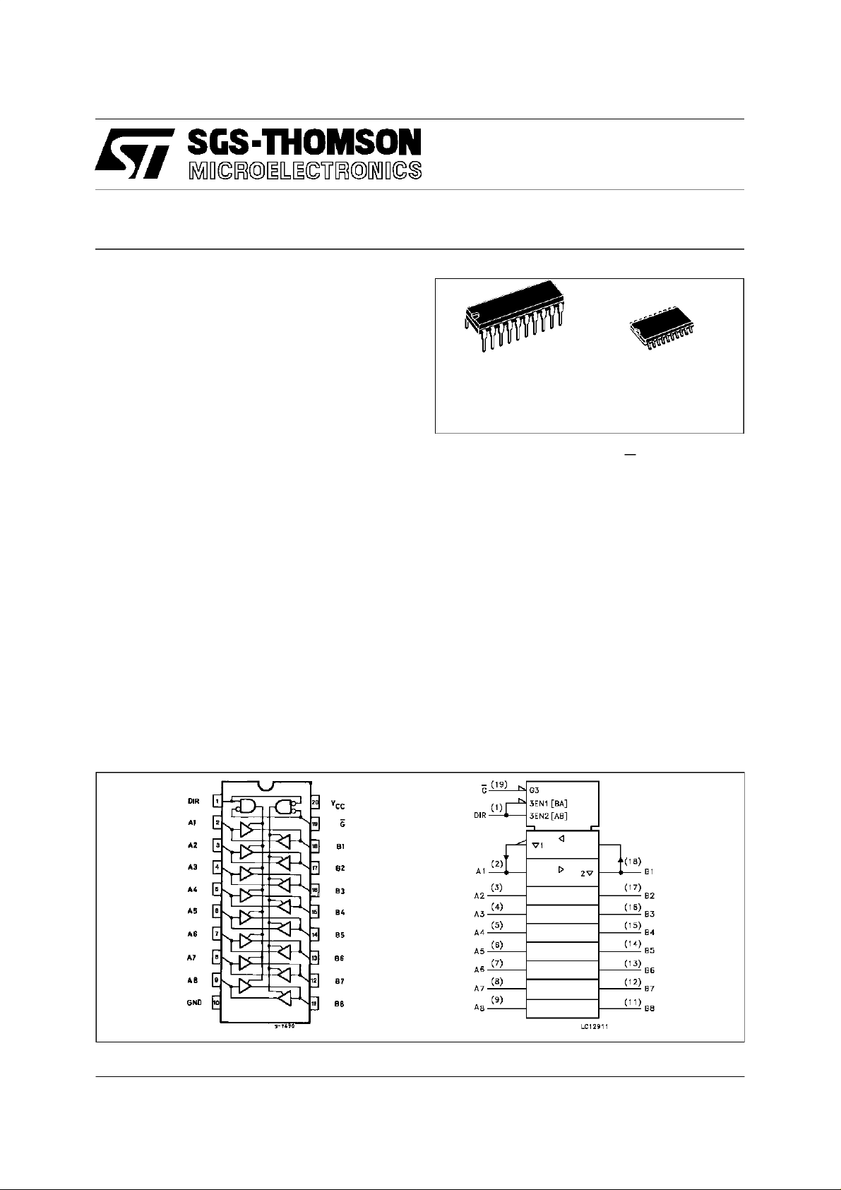
(Plastic Package)
(Micro Package)
M
ORDERCODES:
74AC245B 74AC245M
direction of data trasmission is determined by
DIR input. The enable input G can be used to
disable the device so that the buses are
effectivelyisolated.
All inputs and outputs are equipped with
protectioncircuits against static discharge,giving
them 2KV ESD immunity and transient excess
voltage.
IT IS PROHIBITED TO APPLY A SIGNAL TO A
TERMINAL WHEN IT IS IN OUTPUT MODE
AND WHEN A BUS THERMINAL IS FLOATING
(HIGH IMPEDANCE STATE)IT IS REQUESTED
TO FIX THE INPUT LEVEL BY MEANS OF
EXTERNAL PULL DOWN OR PULL UP
RESISTOR.
PINCONNECTION AND IEC LOGICSYMBOLS
April 1997
1/8
Page 2
74AC245
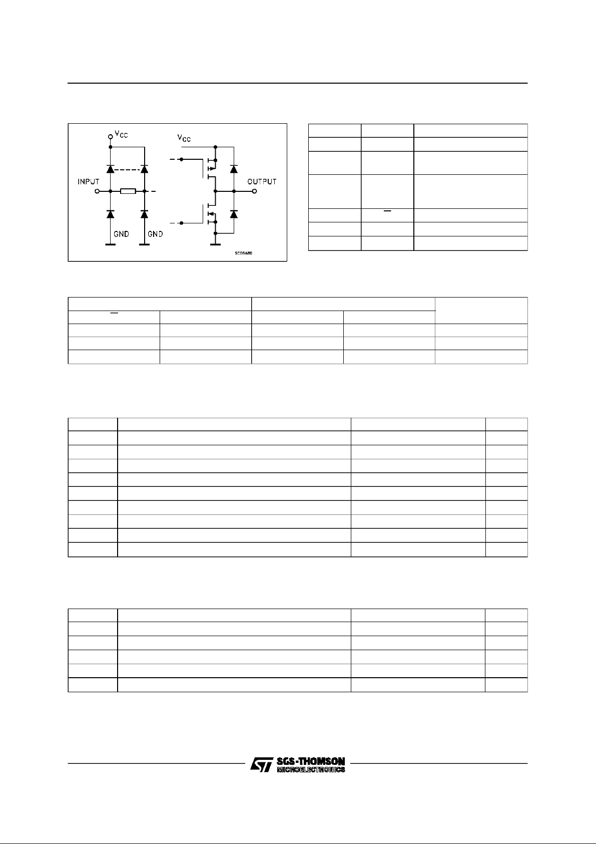
INPUTAND OUTPUTEQUIVALENTCIRCUIT
TRUTH TABLE
INP UT FUNCTI ON OUT PUT
G DIR A BUS B BU S
L L OUTPUT INPUT A = B
L H INPUT OUTPUT B = A
HXZZZ
X:”H”or ”L”
Z: High impedance
PIN DESCRIPTION
PI N N o SYM B O L NAME AND FUNCT I ON
1 DIR Directional Control
2, 3, 4, 5,
6, 7, 8, 9
18, 17, 16,
15, 14, 13,
12, 11
19 G Output Enabel Input
10 GND Ground (0V)
20 V
A1 to A8 Data Inputs/Outputs
B1 to B8 Data Inputs/Outputs
CC
Positive Supply Voltage
ABSOLUTE MAXIMUMRATINGS
Symb o l Parame t er Val u e Uni t
V
V
V
I
I
OK
I
orI
I
CC
T
T
Absolute Maximum Ratings are those values beyond which damage to the device may occur. Functional operation under these condition is not implied.
Supply Voltage -0.5 to +7 V
CC
DC Input Voltage -0.5 to VCC+ 0.5 V
I
DC Output Voltage -0.5 to VCC+ 0.5 V
O
DC Input Diode Current ± 20 mA
IK
DC Output Diode Current ± 20 mA
DC Output Current ± 50 mA
O
DC VCCor Ground Current ± 400 mA
GND
Storage Temperature -65 to +150
stg
Lead Temperature (10 sec) 300
L
o
C
o
C
RECOMMENDEDOPERATINGCONDITIONS
Symb o l Parame t er Value Un i t
V
V
V
T
dt/dv Input Rise and Fall Time V
1) VINfrom30%to70%of V
Supply Voltage 2 to 6 V
CC
Input Voltage 0 to V
I
Output Voltage 0 to V
O
Operating Temperature: -40 to +85
op
= 3.0, 4.5 or 5.5 V(note 1) 8 ns/V
CC
CC
CC
CC
V
V
o
C
2/8
Page 3
DC SPECIFICATIONS
74AC245
Symbol Parameter Test Condition s Value Unit
V
CC
(V)
High Level Input Voltage 3.0 VO= 0.1 V or
V
IH
4.5 3.15 2.25 3.15
V
CC
- 0.1 V
T
=25oC-40to85
A
Min. Typ. Max. Min. Max.
2.1 1.5 2.1
o
C
5.5 3.85 2.75 3.85
Low Level Input Voltage 3.0 VO= 0.1 V or
V
IL
4.5 2.25 1.35 1.35
V
CC
- 0.1 V
1.5 0.9 0.9
5.5 2.75 1.65 1.65
High Level Output
V
OH
Voltage
Low Level Output
V
OL
Voltage
Input Leakage Current
I
I
3 State Output Leakage
I
OZ
Current
Quiescent Supply
I
CC
3.0
4.5 I
5.5 I
V
V
3.0 I
4.5 I
5.5 I
3.0
4.5 I
5.5 I
V
V
3.0 I
4.5 I
5.5 I
5.5
5.5 VI=VIHor V
IO=-50 µA 2.9 2.99 2.9
(*)
I
IH
V
IL
=-50 µA 4.4 4.49 4.4
O
=
=-50 µA 5.4 5.49 5.4
or
O
=-12 mA 2.56 2.46
O
=-24 mA 3.86 3.76
O
=-24 mA 4.86 4.76
O
IO=50 µA 0.002 0.1 0.1
(*)
I
IH
V
IL
=50 µA 0.001 0.1 0.1
O
=
=50 µΑ 0.001 0.1 0.1
or
O
=12 mA 0.36 0.44
O
=24 mA 0.36 0.44
O
=24 mA 0.36 0.44
O
VI=VCCor GND ±0.1 ±1 µA
IL
±0.5 ±5 µA
VO=VCCor GND
5.5 VI=VCCor GND 8 80 µA
Current
Dynamic Output Current
I
OLD
OHD
(note 1, 2)
I
1) Maximum test duration 2ms, one output loaded at time
2) Incident wave switching is guaranteed on transmission lines with impedances aslowas 50 Ω.
(*)All outputs loaded.
5.5 V
= 1.65 V max 75 mA
OLD
V
= 3.85 V min -75 mA
OHD
V
V
V
V
3/8
Page 4

74AC245
AC ELECTRICAL CHARACTERISTICS (CL= 50 pF, RL=500 Ω, Inputtr=tf=3ns)
Symbol Parameter Test Conditi on Value Unit
o
C
ns
ns
ns
t
Propagation Delay Time 3.3
PLH
t
PHL
t
Output Enable Time 3.3
PZL
t
PZH
t
Output Disable Time 3.3
PLZ
t
PHZ
(*) Voltagerangeis 3.3V± 0.3V
(**) Voltagerange is5V± 0.5V
V
5.0
5.0
5.0
(V)
CC
(**)
(**)
(**)
T
=25oC-40to85
A
Min. Typ. Max. Min. Max.
(*)
1.5 5.5 8.5 1.5 9
1.5 4.5 6.5 1.5 7
(*)
1.5 7 12 1.5 13
1.5 5 8.5 1.5 9
(*)
1.5 8.5 12 1.5 13
1.5 6.5 9 1.5 10
CAPACITIVECHARACTERISTICS
Symbol Parameter Test Con ditions Value Uni t
T
V
CC
(V)
Input Capacitance
C
IN
I/O Capacitance
C
i/o
Power Dissipation
C
PD
5.0
5.0
5.0 20 pF
Capacitance (note 1)
1)CPDisdefined as the value of the IC’s internal equivalent capacitance which is calculated from the operating current consumption without load. (Refer to
Test Circuit). Average operating current can be obtained bythe following equation. I
(opr)= CPD•VCC•fIN+ICC/n(percircuit)
CC
=25oC -40 to 85oC
A
Min. Typ. Max. Mi n . Max.
5
10
pF
pF
TEST CIRCUIT
TEST SWITCH
t
PLH,tPHL
t
PZL,tPLZ
t
PZH,tPHZ
CL= 50 pF or equivalent (includes jig and probe capacitance)
R
= 500Ω or equivalent
L=R1
R
of pulse generator (typically 50Ω)
T=ZOUT
Open
2V
CC
Open
4/8
Page 5

WAVEFORM 1: PROPAGATIONDELAYS (f=1MHz;50% duty cycle)
74AC245
WAVEFORM 2: OUTPUTENABLE AND DISABLE TIME(f=1MHz;50%duty cycle)
5/8
Page 6

74AC245
Plastic DIP20 (0.25) MECHANICAL DATA
DIM.
MIN. TYP. MAX. MIN. TYP. MAX.
a1 0.254 0.010
B 1.39 1.65 0.055 0.065
b 0.45 0.018
b1 0.25 0.010
D 25.4 1.000
E 8.5 0.335
e 2.54 0.100
e3 22.86 0.900
F 7.1 0.280
I 3.93 0.155
L 3.3 0.130
Z 1.34 0.053
mm inch
6/8
P001J
Page 7

SO20 MECHANICAL DATA
74AC245
DIM.
MIN. TYP. MAX. MIN. TYP. MAX.
A 2.65 0.104
a1 0.10 0.20 0.004 0.007
a2 2.45 0.096
b 0.35 0.49 0.013 0.019
b1 0.23 0.32 0.009 0.012
C 0.50 0.020
c1 45° (typ.)
D 12.60 13.00 0.496 0.512
E 10.00 10.65 0.393 0.419
e 1.27 0.050
e3 11.43 0.450
F 7.40 7.60 0.291 0.299
L 0.50 1.27 0.19 0.050
M 0.75 0.029
S8°(max.)
mm inch
P013L
7/8
Page 8

74AC245
Information furnished is believed to be accurate and reliable. However,SGS-THOMSON Microelectronicsassumesno responsability for the
consequencesof use ofsuch information nor for anyinfringement of patentsor other rights ofthird parties whichmay results from its use. No
licenseisgrantedby implicationor otherwise underany patentor patent rights ofSGS-THOMSONMicroelectronics.Specificationsmentioned
in this publicationare subjectto change without notice.This publication supersedes andreplaces all informationpreviously supplied.
SGS-THOMSONMicroelectronicsproductsarenotauthorized foruseas criticalcomponents in lifesupportdevicesor systemswithoutexpress
writtenapproval of SGS-THOMSONMicroelectonics.
1997 SGS-THOMSONMicroelectronics- Printedin Italy- AllRights Reserved
Australia- Brazil - Canada- China- France- Germany- HongKong - Italy- Japan- Korea- Malaysia- Malta- Morocco- TheNetherlands -
Singapore- Spain- Sweden- Switzerland- Taiwan - Thailand - United Kingdom- U.S.A
SGS-THOMSONMicroelectronics GROUPOF COMPANIES
.
8/8
 Loading...