

Page 1
74AC244
OCTAL BUS BUFFER
WITH 3 STATE OUTPUTS (NON INVERTED)
■ HIGH SPEED: t
■ LOWPOWER DISSIPATION:
=8µA (MAX.)at TA=25oC
I
CC
■ HIGH NOISE IMMUNITY:
V
NIH=VNIL
■ 50Ω TRANSMISSION LINE DRIVING
=4 ns (TYP.)atVCC=5V
PD
=28%VCC(MIN.)
CAPABILITY
■ SYMMETRICAL OUTPUT IMPEDANCE:
|I
|=IOL=24mA(MIN)
OH
■ BALANCE DPROPAGATIONDELAYS:
t
≅ t
PLH
PHL
■ OPERATINGVOLTAGERAN GE:
V
(OPR) = 2V to 6V
CC
■ PIN AND FUNCTION COMPATIBLE WITH
74SERIES244
■ IMPROVED LATCH-UP IMMUNITY
DESCRIPTION
The AC244 is an advanced CMOS OCTAL BUS
BUFFER (3-STATE) fabricated with sub-micron
silicon gate and double-layermetal wiring C
2
MOS
technology. It is ideal for low power applications
B
(Plastic Package)
(Micro Package)
M
ORDERCODES:
74AC244B 74AC244M
mantaining high speed operation similar to
equivalentBipolarSchottky TTL.
G controloutput governs four BUS BUFFERs.
This device is desibned to be used with 3 state
memoryaddress drivers,etc.
All inputs and outputs are equipped with
protectioncircuits against static discharge, giving
them 2KV ESD immunity and transient excess
voltage.
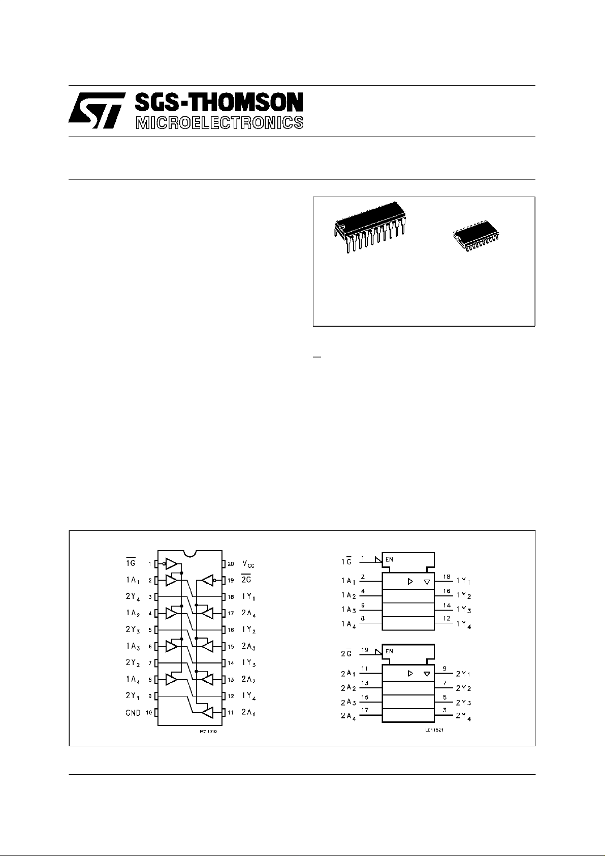
PINCONNECTION AND IEC LOGIC SYMBOLS
April 1997
1/8
Page 2
74AC244
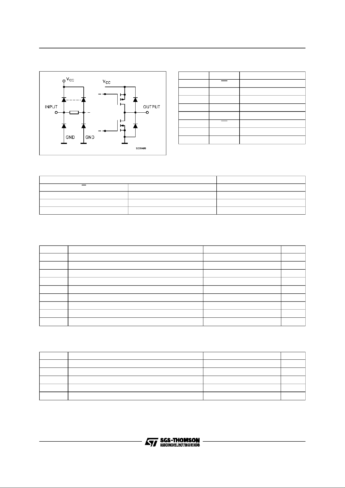
INPUTAND OUTPUTEQUIVALENTCIRCUIT
TRUTH TABLE
INPUT OUTPUT
GAnYn
LLL
LHH
HXZ
X:”H”or ”L”
Z: High impedance
PIN DESCRIPTION
PI N No SYM B O L NAME A ND FUNC T I ON
1 1G Output Enable Input
2,4, 6,8 1A1to1A4 Data Inputs
9,7, 5,3 2Y1to2Y4 Data Outputs
11,13,15, 17 2A1to2A4 Data Inputs
18,16,14, 12 1Y1to1Y4 Data Outputs
19 2G Output Enabel Input
10 GND Ground (0V)
20 V
CC
Positive Supply Voltage
ABSOLUTE MAXIMUM RATINGS
Symb o l Parame t er Val u e Uni t
V
V
V
I
I
OK
I
orI
I
CC
T
T
Absolute Maximum Ratings are those values beyond which damage to the device may occur. Functional operation under these condition is not implied.
Supply Voltage -0.5to+7 V
CC
DC Input Voltage -0.5toVCC+0.5 V
I
DC Output Voltage -0.5toVCC+0.5 V
O
DC Input Diode Current ± 20 mA
IK
DC Output Diode Current ± 20 mA
DC Output Current ± 50 mA
O
DC VCCor Ground Current ± 400 mA
GND
Storage Temperature -65to+150
stg
Lead Temperature (10 sec) 300
L
o
C
o
C
RECOMMENDED OPERATINGCONDITIONS
Symb o l Parame t er Value Un i t
V
V
V
T
dt/dv Input Rise and Fall Time V
1) VINfrom30%to 70%of V
Supply Voltage 2to6 V
CC
Input Voltage 0toV
I
Output Voltage 0toV
O
Operating Temperature: -40to+85
op
= 3.0, 4.5 or 5.5 V(note 1) 8 ns/V
CC
CC
CC
CC
V
V
o
C
2/8
Page 3
DC SPECIFICATIONS
74AC244
Symbol Parameter Test Condit ions Value Unit
V
CC
(V)
High Level Input Voltage 3.0 VO=0.1V or
V
IH
4.5 3.15 2.25 3.15
T
=25oC-40to85
A
Min. Typ. Ma x. Min . Max.
2.1 1.5 2.1
V
-0.1V
CC
o
C
5.5 3.85 2.75 3.85
Low Level Input Voltage 3.0 VO=0.1V or
V
IL
4.5 2.25 1.35 1.35
V
-0.1V
CC
1.5 0.9 0.9
5.5 2.75 1.65 1.65
High Level Output
V
OH
Voltage
Low Level Output
V
OL
Voltage
Input Leakage Current
I
I
3 State Output Leakage
I
OZ
Current
Quiescent Supply
I
CC
3.0
4.5 I
5.5 I
3.0 I
V
I
V
IH
V
4.5 I
5.5 I
3.0
4.5 I
5.5 I
3.0 I
V
I
V
IH
V
4.5 I
5.5 I
5.5
5.5 VI=VIHor V
IO=-50µA 2.9 2.99 2.9
(*)
or
IL
=-50µA 4.4 4.49 4.4
O
=
=-50µA 5.4 5.49 5.4
O
=-12 mA 2.56 2.46
O
=-24 mA 3.86 3.76
O
=-24 mA 4.86 4.76
O
IO=50µA0.0020.1 0.1
(*)
=
or
IL
=50µA0.0010.1 0.1
O
=50µΑ 0.001 0.1 0.1
O
=12mA 0.36 0.44
O
=24mA 0.36 0.44
O
=24mA 0.36 0.44
O
VI=VCCorGND ±0.1 ±1 µA
IL
±0.5 ±5 µA
VO=VCCorGND
5.5 VI=VCCorGND 8 80 µA
Current
Dynamic Output Current
I
OLD
(note 1, 2)
I
OHD
1) Maximum test duration 2ms, one output loaded at time
2) Incident wave switching is guaranteed on transmission lines with impedances as low as 50 Ω.
(*)All outputs loaded.
5.5 V
=1.65 Vmax 75 mA
OLD
V
=3.85Vmin -75 mA
OHD
V
V
V
V
3/8
Page 4

74AC244
AC ELECTRICAL CHARACTERISTICS (CL= 50 pF, RL=500 Ω, Inputtr=tf=3ns)
Symbol Parameter Test Conditi on Value Unit
o
C
ns
ns
ns
t
Propagation Delay Time 3.3
PLH
t
PHL
t
Output Enable Time 3.3
PZL
t
PZH
t
Output Disable Time 3.3
PLZ
t
PHZ
(*) Voltagerange is3.3V± 0.3V
(**) Voltagerangeis5V±0.5V
V
(V)
5.0
5.0
5.0
CC
T
=25oC-40to85
A
Min. Typ. Ma x. Min . Max.
(*)
(**)
(*)
(**)
(*)
(**)
1.5 5 9 1.5 10
1.5 4 7 1.5 7.5
1.5 6 10 1.5 11
1.5 4 8 1.5 8.5
1.5 7 11 1.5 12
1.5 5.5 9 1.5 10
CAPACITIVE CHARACTERISTICS
Symbol Para met er Test C o n dit ion s V al u e Uni t
T
V
CC
(V)
Input Capacitance
C
IN
C
Output Capacitance
OUT
Power Dissipation
C
PD
5.0
5.0
5.0 21 pF
Capacitance (note 1)
1)CPDisdefined as the value of the IC’s internal equivalent capacitance which is calculated from the operating current consumption without load. (Refer to
Test Circuit). Average operating current can be obtained by the following equation. I
(opr)= CPD•VCC•fIN+ICC/n(percircuit)
CC
=25oC -40 to 85oC
A
Min. Typ. Max. M i n . Max.
4
8
pF
pF
TEST CIRCUIT
TEST SWITCH
t
PLH,tPHL
t
PZL,tPLZ
t
PZH,tPHZ
CL= 50 pF or equivalent (includes jig and probe capacitance)
R
= 500Ω or equivalent
L=R1
R
of pulse generator (typically 50Ω)
T=ZOUT
Open
2V
CC
Open
4/8
Page 5

WAVEFORM 1: PROPAGATIONDELAYS (f=1MHz;50% duty cycle)
74AC244
WAVEFORM 2: OUTPUT ENABLE AND DISABLE TIME (f=1MHz; 50% duty cycle)
5/8
Page 6

74AC244
Plastic DIP20 (0.25) MECHANICAL DATA
DIM.
MIN. TYP. MAX. MIN. TYP. MAX.
a1 0.254 0.010
B 1.39 1.65 0.055 0.065
b 0.45 0.018
b1 0.25 0.010
D 25.4 1.000
E 8.5 0.335
e 2.54 0.100
e3 22.86 0.900
F 7.1 0.280
I 3.93 0.155
L 3.3 0.130
Z 1.34 0.053
mm inch
6/8
P001J
Page 7

SO20 MECHANICAL DATA
74AC244
DIM.
MIN. TYP. MAX. MIN. TYP. MAX.
A 2.65 0.104
a1 0.10 0.20 0.004 0.007
a2 2.45 0.096
b 0.35 0.49 0.013 0.019
b1 0.23 0.32 0.009 0.012
C 0.50 0.020
c1 45° (typ.)
D 12.60 13.00 0.496 0.512
E 10.00 10.65 0.393 0.419
e 1.27 0.050
e3 11.43 0.450
F 7.40 7.60 0.291 0.299
L 0.50 1.27 0.19 0.050
M 0.75 0.029
S8°(max.)
mm inch
P013L
7/8
Page 8

74AC244
Information furnished is believedtobe accurateandreliable.However,SGS-THOMSON Microelectronicsassumesno responsability for the
consequencesof use ofsuch informationnor for any infringement of patents or otherrights of third parties which may resultsfromitsuse.No
licenseisgrantedby implicationor otherwise underany patentorpatent rightsofSGS-THOMSONMicroelectronics.Specificationsmentioned
in this publicationare subjecttochange withoutnotice.This publication supersedes and replaces all informationpreviously supplied.
SGS-THOMSONMicroelectronics productsare notauthorizedfor useas criticalcomponents in lifesupportdevices or systems withoutexpress
writtenapproval of SGS-THOMSON Microelectonics.
1997 SGS-THOMSONMicroelectronics- Printedin Italy - All Rights Reserved
Australia- Brazil - Canada - China- France- Germany - Hong Kong- Italy- Japan- Korea- Malaysia- Malta - Morocco- TheNetherlands-
Singapore- Spain- Sweden- Switzerland-Taiwan- Thailand - United Kingdom - U.S.A
SGS-THOMSONMicroelectronics GROUPOF COMPANIES
.
8/8
 Loading...