

Page 1
■ HIGH SPEED:t
■ LOWPOWERDISSIPATION:
=4µA (MAX.)at TA=25oC
I
CC
■ HIGH NOISE IMMUNITY:
V
NIH=VNIL
■ 50Ω TRANSMISSION LINE DRIVING
=4 ns(TYP.)atVCC=5V
PD
=28%VCC(MIN.)
CAPABILITY
■ SYMMETRICAL OUTPUT IMPEDANCE:
|I
|=IOL=24 mA (MIN)
OH
■ BALANCE DPROPAGATIONDELAYS:
t
≅ t
PLH
PHL
■ OPERATINGVOLTAGERANGE:
V
(OPR) = 2V to 6V
CC
■ PIN AND FUNCTION COMPATIBLE WITH
74SERIES20
■ IMPROVED LATCH-UP IMMUNITY
DESCRIPTION
The AC20 is an advanced high-speed CMOS
DUAL 4-INPUT NAND GATE fabricated with
sub-micron silicon gate and double-layer metal
74AC20
DUAL 4-INPUT NAND GATE
PRELIMINARY DATA
B
(Plastic Package)
(Micro Package)
ORDERCODES:
74AC20B 74AC20M
wiring C
2
MOS technology. It is ideal for low
power applications mantaining high speed
operation similar to equivalent Bipolar Schottky
TTL.
The internal circuit is composed of 3 stages
including buffer output, which enables high noise
immunityand stable output.
All inputs and outputs are equipped with
protectioncircuits against static discharge, giving
them 2KV ESD immunity and transient excess
voltage.
M
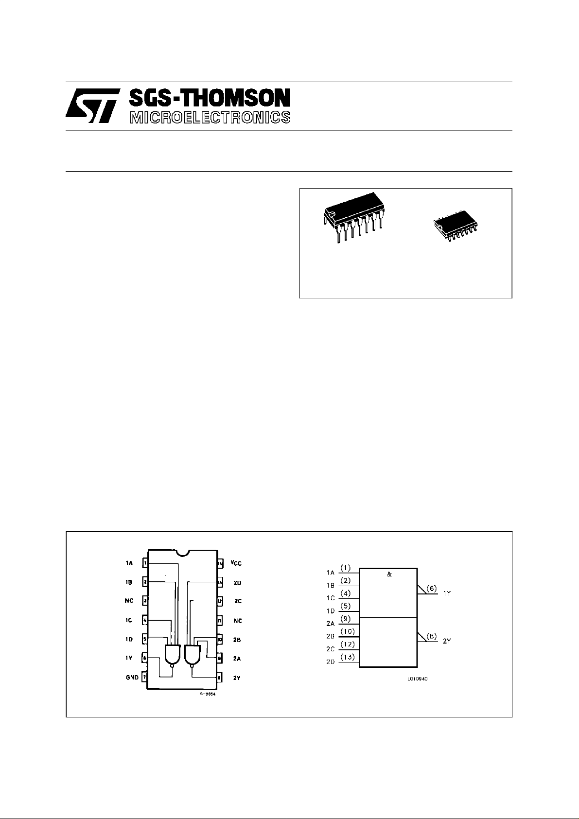
PINCONNECTION ANDIEC LOGICSYMBOLS
May 1997
1/7
Page 2
74AC20
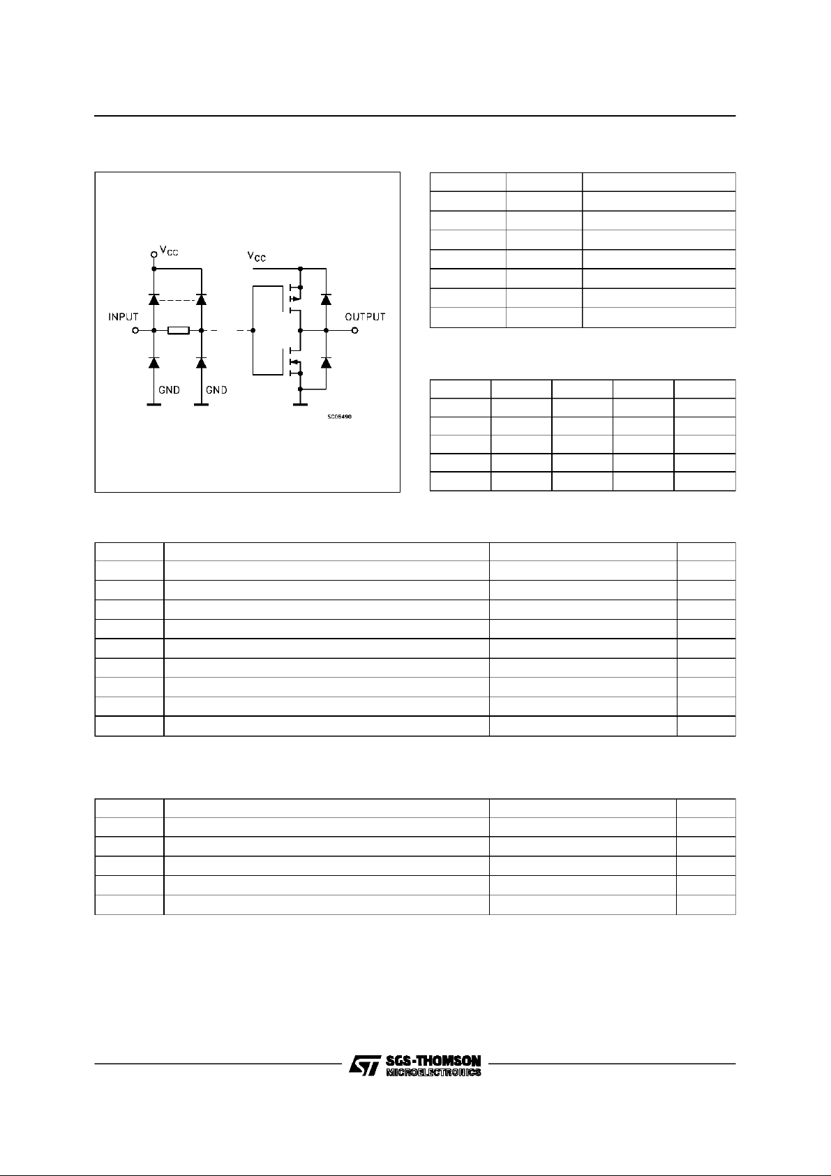
INPUTAND OUTPUT EQUIVALENTCIRCUIT
PIN DESCRIPTION
PI N No SYM B O L NAME AN D FUNC T I ON
1, 9 1A to 2A Data Inputs
2, 10 1B to 2B Data Inputs
3, 11 1C to 2C Data Inputs
5, 13 1D to 2D Data Inputs
6, 8 1Y to 2Y Data Outputs
7 GND Ground (0V)
14 V
CC
Positive Supply Voltage
TRUTHTABLE
ABCCY
LXXXH
XLXXH
XXLXH
XXXLH
HHHHL
ABSOLUTE MAXIMUM RATINGS
Symb o l Parame t er Val u e Uni t
V
V
V
I
I
OK
I
orI
I
CC
T
T
Absolute Maximum Ratings are those values beyond which damage to the device may occur. Functional operation under these condition is not implied.
Supply Voltage -0.5 to +7 V
CC
DC Input Voltage -0.5 to VCC+ 0.5 V
I
DC Output Voltage -0.5 to VCC+ 0.5 V
O
DC Input Diode Current ± 20 mA
IK
DC Output Diode Current ± 20 mA
DC Output Current ± 50 mA
O
DC VCCor Ground Current ± 100 mA
GND
Storage Temperature -65 to +150
stg
Lead Temperature (10 sec) 300
L
o
C
o
C
RECOMMENDED OPERATING CONDITIONS
Symb o l Parame t er Value Un i t
V
V
V
T
dt/dv Input Rise and Fall Time V
1) VINfrom30%to70%of V
2/7
Supply Voltage 2 to 6 V
CC
Input Voltage 0 to V
I
Output Voltage 0 to V
O
Operating Temperature: -40 to +85
op
= 3.0, 4.5 or 5.5 V(note 1) 8 ns/V
CC
CC
CC
CC
V
V
o
C
Page 3
DC SPECIFICATIONS
74AC20
Symbol Parameter Test Condition s Value Unit
V
CC
(V)
High Level Input Voltage 3.0 VO= 0.1 V or
V
IH
4.5 3.15 2.25 3.15
V
CC
- 0.1 V
T
=25oC-40to85
A
Min. Typ. Max. Min . Max.
2.1 1.5 2.1
o
C
5.5 3.85 2.75 3.85
Low Level Input Voltage 3.0 VO= 0.1 V or
V
IL
4.5 2.25 1.35 1.35
V
CC
- 0.1 V
1.5 0.9 0.9
5.5 2.75 1.65 1.65
High Level Output
V
OH
Voltage
Low Level Output
V
OL
Voltage
Input Leakage Current
I
I
Quiescent Supply
I
CC
3.0
4.5 I
5.5 I
V
V
3.0 I
4.5 I
5.5 I
3.0
4.5 I
5.5 I
V
V
3.0 I
4.5 I
5.5 I
5.5
IO=-50 µA 2.9 2.99 2.9
(*)
I
IH
V
IL
=-50 µA 4.4 4.49 4.4
O
=
=-50 µA 5.4 5.49 5.4
or
O
=-12 mA 2.56 2.46
O
=-24 mA 3.86 3.76
O
=-24 mA 4.86 4.76
O
IO=50 µA 0.002 0.1 0.1
(*)
I
IH
V
IL
=50 µA 0.001 0.1 0.1
O
=
=50 µA 0.001 0.1 0.1
or
O
=12 mA 0.36 0.44
O
=24 mA 0.36 0.44
O
=24 mA 0.36 0.44
O
VI=VCCor GND ±0.1 ±1 µA
5.5 VI=VCCor GND 4 40 µA
Current
Dynamic Output Current
I
OLD
OHD
(note 1, 2)
I
1) Maximum test duration 2ms, one output loaded at time
2) Incident wave switching is guaranteed on transmission lines with impedances as low as 50 Ω.
(*)All outputs loaded.
5.5 V
= 1.65 Vmax 75 mA
OLD
V
= 3.85 V min -75 mA
OHD
V
V
V
V
AC ELECTRICAL CHARACTERISTICS (CL= 50 pF, RL=500 Ω, Inputtr=tf=3ns)
Symbol Parameter Test Cond ition Value Unit
t
Propagation Delay Time 3.3
PLH
t
PHL
(*) Voltage rangeis3.3V ± 0.3V
(**) Voltagerange is5V± 0.5V
V
5.0
CC
(V)
(*)
(**)
T
=25oC-40to85
A
Min. Typ. Max. Min . Max.
1.5 5.0 7.0 1.0 9.0
1.5 4.0 6.0 1.0 7.0
o
C
ns
CAPACITIVE CHARACTERISTICS
Symbol Parameter Test Condition s Value Unit
=25oC-40to85
T
A
Min. Typ. Max. Min . Max.
4.5
Input Capacitance
C
IN
Power Dissipation
C
PD
V
CC
(V)
5.0
5.0 40 pF
Capacitance (note 1)
1) CPDis defined as the value of the IC’s internal equivalent capacitance which is calculated from the operating current consumption without load. (Refer to
Test Circuit). Average operating current can be obtained by the following equation. I
(opr)=CPD• VCC•fIN+ICC/n (percircuit)
CC
o
C
pF
3/7
Page 4

74AC20
TEST CIRCUIT
CL= 50 pF or equivalent (includes jig and probe capacitance)
= 500Ω or equivalent
R
L=R1
R
WAVEFORM: PROPAGATION DELAYS (f=1MHz; 50%duty cycle)
of pulse generator (typically 50Ω)
T=ZOUT
4/7
Page 5

Plastic DIP-14 MECHANICAL DATA
74AC20
DIM.
MIN. TYP. MAX. MIN. TYP. MAX.
a1 0.51 0.020
B 1.39 1.65 0.055 0.065
b 0.5 0.020
b1 0.25 0.010
D 20 0.787
E 8.5 0.335
e 2.54 0.100
e3 15.24 0.600
F 7.1 0.280
I 5.1 0.201
L 3.3 0.130
Z 1.27 2.54 0.050 0.100
mm inch
P001A
5/7
Page 6

74AC20
SO-14 MECHANICAL DATA
DIM.
MIN. TYP. MAX. MIN. TYP. MAX.
A 1.75 0.068
a1 0.1 0.2 0.003 0.007
a2 1.65 0.064
b 0.35 0.46 0.013 0.018
b1 0.19 0.25 0.007 0.010
C 0.5 0.019
c1 45 (typ.)
D 8.55 8.75 0.336 0.344
E 5.8 6.2 0.228 0.244
e 1.27 0.050
e3 7.62 0.300
F 3.8 4.0 0.149 0.157
G 4.6 5.3 0.181 0.208
L 0.5 1.27 0.019 0.050
M 0.68 0.026
S 8 (max.)
mm inch
6/7
P013G
Page 7

74AC20
Information furnishedis believed to be accurate and reliable. However, SGS-THOMSON Microelectronics assumes no responsability for the
consequencesof use of such information nor for any infringement of patents or other rights of third parties whichmay resultsfrom itsuse. No
licenseis grantedby implication or otherwise underany patent or patentrights ofSGS-THOMSONMicroelectronics. Specificationsmentioned
in this publication are subject to change without notice. This publication supersedes and replaces all information previously supplied.
SGS-THOMSONMicroelectronics productsare notauthorized foruse as criticalcomponents inlifesupportdevicesor systems withoutexpress
writtenapproval of SGS-THOMSON Microelectonics.
1997 SGS-THOMSONMicroelectronics - Printedin Italy - All Rights Reserved
Australia- Brazil - Canada - China- France- Germany- HongKong - Italy- Japan- Korea- Malaysia- Malta - Morocco- TheNetherlands-
Singapore- Spain- Sweden- Switzerland - Taiwan -Thailand - United Kingdom - U.S.A
SGS-THOMSONMicroelectronics GROUPOF COMPANIES
.
7/7
 Loading...