

Datasheet 74AC174MTCX, 74AC174MTC, 74AC174CW, 74AC174SJX, 74AC174SJ Datasheet (Fairchild Semiconductor)
...Page 1
© 1999 Fairchild Semiconductor Corporation DS009935 www.fairchildsemi.com
November 1988
Revised November 1999
74AC174 • 74ACT174 Hex D-Type Flip-Flop with Master Reset
74AC174 • 74ACT174
Hex D-Type Flip-Flop with Master Reset
General Description
The AC/ACT174 is a high-sp eed hex D-type flip-flo p. The
device is used pr imarily as a 6-bit edge-triggered sto rage
register. The information on the D inp uts is transferred to
storage during the LOW-to-HIGH clock transition. The
device has a Master Reset t o simultaneously cl ear all flipflops.
Features
■ ICC reduced by 50%
■ Outputs source/sink 24 mA
■ ACT174 has TTL-compatible inputs
Ordering Code:
Device also available in Tape and Reel. Specify by appending s uffix let te r “X” to the ordering code.
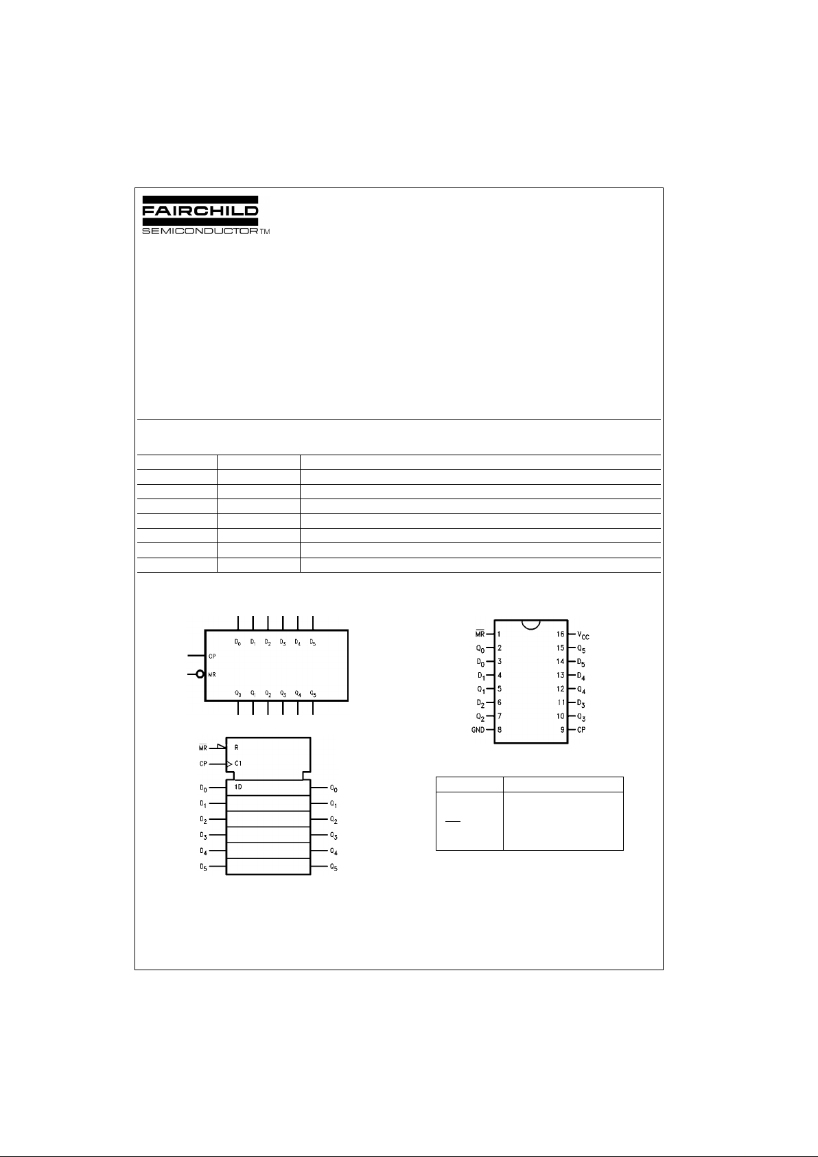
Logic Symbols
IEEE/IEC
Connection Diagram
Pin Descriptions
FACT is a trademark of Fairchild Semiconductor Corporation.
Order Number Package Number Package Description
74AC174SC M16A 16-Lead Small Outline Integrated Circuit (SOIC), JEDEC MS-012, 0.150” Narrow Body
74AC174SJ M16D 16-Lead Small Outline Package (SOP), EIAJ TYPE II, 5.3mm Wide
74AC174PC N16E 16-Lead Plastic Dual-In-Line Package (PDIP), JEDEC MS-001, 0.300” Wide
74ACT174SC M16A 16-Lead Small Outline Integrated Circuit (SOIC), JEDEC MS-012, 0.150” Narrow
74ACT174SJ M16D 16-Lead Small Outline Package (SOP), EIAJ TYPE II, 5.3mm Wide
74ACT174MTC MTC16 16-Lead Thin Shrink Small Outline Package (TSSOP), JEDEC MO-153, 4.4mm Wide
74ACT174PC N16E 16-Lead Plastic Dual-In-Line Package (PDIP), JEDEC MS-001, 0.300” Wide
Pin Names Description
D
0–D5
Data Inputs
CP Clock Pulse Input
MR Master Reset Input
Q
0–Q5
Outputs
Page 2
www.fairchildsemi.com 2
74AC174 • 74ACT174
Functional Description
The AC/ACT174 consists o f six edge-tri ggered D-t ype flipflops with individual D inputs and Q outputs. The Clock
(CP) and Master Reset (MR
) are common to all flip-flops.
Each D input’s state is transferred to the corresponding flipflop’s output following the LOW-to-HIGH Clock (CP) transition. A LOW input to the Ma ster Reset (MR
) will force all
outputs LOW independent of Clock or Data inputs. The AC/
ACT174 is useful for applications where the true output
only is required an d the Clock and Master R eset are com mon to all storage elements.
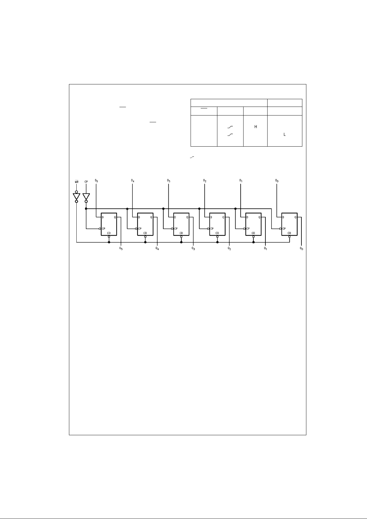
Tr uth Table
H = HIGH Voltage Level
L = LOW Voltage Level
= LOW-to-HIGH Transition
X = Immaterial
Logic Diagram
Please note that this diagram is provided only for the understanding of logic operations and should not be used to estimate propagation delays.
Inputs Output
MR CP D Q
LX X L
H
HH
H
LL
HL X Q
Page 3
3 www.fairchildsemi.com
74AC174 • 74ACT174
Absolute Maximum Ratings(Note 1) Recommended Operating
Conditions
Note 1: Absolute max imum ratings are those values beyond w hich damage
to the device may occu r. The databook spe cificatio ns shou ld be met, wit hout exception, to ensure that the system de sign is relia ble over its p ower
supply, temperature, and output/input loading variables. Fairchild does not
recommend operation of FACT circuits outside databook specif ic at ions.
DC Electrical Characteristics for AC
Note 2: All outputs loaded; thres holds on input associate d w it h output under test.
Note 3: Maximum test duration 2.0 ms, one output loaded at a time.
Note 4: I
IN
and ICC @ 3.0V are guaranteed to be less than or equa l t o th e respective limit @ 5.5V VCC.
Supply Voltage (VCC) −0.5V to +7.0V
DC Input Diode Current (I
IK
)
V
I
= −0.5V −20 mA
V
I
= VCC + 0.5V +20 mA
DC Input Voltage (V
I
) −0.5V to VCC + 0.5V
DC Output Diode Current (I
OK
)
V
O
= −0.5V −20 mA
V = V
CC
+ 0.5V +20 mA
DC Output Voltage (V
O
) −0.5V to V
CC
+ 0.5V
DC Output S ource
or Sink Current (I
O
) ±50 mA
DC V
CC
or Ground Current
per Output Pin (I
CC
or I
GND
) ±50 mA
Storage Temperature (T
STG
) −65°C to +150°C
Junction Temperature (T
J
)
PDIP 140°C
Supply Voltage (V
CC
)
AC 2.0V to 6.0V
ACT 4.5V to 5.5V
Input Voltage (V
I
)0V to V
CC
Output Voltage (VO)0V to V
CC
Operating Temperature (TA) −40°C to +85°C
Minimum Input Edge Rate (∆V/∆t)
AC Devices
V
IN
from 30% to 70% of V
CC
VCC @ 3.3V, 4.5V, 5.5V 125 mV/ns
Minimum Input Edge Rate (∆V/∆t)
ACT Devices
V
IN
from 0.8V to 2.0V
V
CC
@ 4.5V, 5.5V 125 mV/ns
Symbol Parameter
V
CC
TA = +25°C TA = −40°C to +85°C
Units Conditions
(V) Typ Guaranteed Limits
V
IH
Minimum HIGH Level 3.0 1.5 2.1 2.1 V
OUT
= 0.1V
Input Voltage 4.5 2.25 3.15 3.15 V or VCC − 0.1V
5.5 2.75 3.85 3.85
V
IL
Maximum LOW Level 3.0 1.5 0.9 0.9 V
OUT
= 0.1V
Input Voltage 4.5 2.25 1.35 1.35 V or VCC − 0.1V
5.5 2.75 1.65 1.65
V
OH
Minimum HIGH Level 3.0 2.99 2.9 2.9
Output Voltage 4.5 4.49 4.4 4.4 V I
OUT
= −50 µA
5.5 5.49 5.4 5.4
VIN = VIL or V
IH
3.0 2.56 2.46 IOH = −12 mA
4.5 3.86 3.76 V I
OH
= −24 mA
5.5 4.86 4.76 I
OH
= −24 mA (Note 2)
V
OL
Maximum LOW Level 3.0 0.002 0.1 0.1
Output Voltage 4.5 0.001 0.1 0.1 V I
OUT
= 50 µA
5.5 0.001 0.1 0.1
VIN = VIL or V
IH
3.0 0.36 0.44 IOL = 12 mA
4.5 0.36 0.44 V IOL = 24 mA
5.5 0.36 0.44 IOL = 24 mA (Note 2)
I
IN
Maximum Input
5.5 ±0.1 ±1.0 µA
VI = V
CC
(Note 4) Leakage Current or GND
I
OLD
Minimum Dynamic 5.5 75 mA V
OLD
= 1.65V Max
I
OHD
Output Current (Note 3) 5.5 −75 mA V
OHD
= 3.85V Min
I
CC
Maximum Quiescent
5.5 4.0 40.0 µA
VIN = V
CC
(Note 4) Supply Current or GND
Page 4

www.fairchildsemi.com 4
74AC174 • 74ACT174
DC Electrical Characteristics for ACT
Note 5: All outputs loaded; thresholds on input assoc iat ed with output under tes t.
Note 6: Maximum test duratio n 2. 0 ms, one output loaded at a time.
AC Electrical Characteristics for AC
Note 7: Voltage Range 3.3 is 3.3V ± 0.3V
Voltage Range 5.0 is 5.0V ± 0.5V
Symbol Parameter
V
CC
TA = +25°CT
A
= −40°C to +85°C
Units Conditions
(V) Typ Guaranteed Limits
V
IH
Minimum HIGH Level 4.5 1.5 2.0 2.0
V
V
OUT
= 0.1V
Input Voltage 5.5 1.5 2.0 2.0 or VCC − 0.1V
V
IL
Maximum LOW Level 4.5 1.5 0.8 0.8
V
V
OUT
= 0.1V
Input Voltage 5.5 1.5 0.8 0.8 or V
CC
− 0.1V
V
OH
Minimum HIGH Level 4.5 4.49 4.4 4.4
VI
OUT
= −50 µA
Output Voltage 5.5 5.49 5.4 5.4
VIN = VIL or V
IH
4.5 3.86 3.76 V IOH = −24 mA
5.5 4.86 4.76 I
OH
= −24 mA (Note 5)
V
OL
Maximum LOW Level 4.5 0.001 0.1 0.1
VI
OUT
= 50 µA
Output Voltage 5.5 0.001 0.1 0.1
VIN = V
IL
or V
IH
4.5 0.36 0.44 V IOL = 24 mA
5.5 0.36 0.44 IOL = 24 mA (Note 5)
I
IN
Maximum Input
5.5 ±0.1 ±1.0 µAVI = VCC, GND
Leakage Current
I
CCT
Maximum
5.5 0.6 1.5 mA VI = VCC − 2.1V
ICC/Input
I
OLD
Minimum Dynamic 5.5 75 mA V
OLD
= 1.65V Max
I
OHD
Output Current (Note 6) 5.5 −75 mA V
OHD
= 3.85V Min
I
CC
Maximum Quiescent
5.5 4.0 40.0 µA
VIN = V
CC
Supply Current or GND
Symbol Parameter
V
CC
(V)
(Note 7)
TA = +25°C
C
L
= 50 pF
T
A
= −40°C to +85°C
C
L
= 50 pF
Units
Min Typ Max Min Max
f
MAX
Maximum Clock 3.3 90 100 70
MHz
Frequency 5.0 100 125 100
t
PLH
Propagation Delay 3.3 2.0 9.0 11.5 1.5 12.5
ns
CP to Q
n
5.0 1.5 6.0 8.5 1.0 9.5
t
PHL
Propagation Delay 3.3 2.0 8.5 11.0 1.5 12.0
ns
CP to Q
n
5.0 1.5 6.0 8.0 1.0 9.0
t
PHL
Propagation Delay 3.3 2.5 9.0 11.5 2.0 12.5
ns
MR to Q
n
5.0 1.5 7.0 9.0 1.5 10.5
Page 5

5 www.fairchildsemi.com
74AC174 • 74ACT174
AC Operating Requirements for AC
Note 8: Voltage Range 3.3 is 3.3V ± 0.3V
Voltage Range 5.0 is 5.0V ± 0.5V
AC Electrical Characteristics for ACT
Note 9: Voltage Range 5.0 is 5.0V ± 0.5V
AC Operating Requirements for ACT
Note 10: Voltage Ran ge 5.0 is 5.0V ± 0.5V
Capacitance
Symbol Parameter
V
CC
(V)
(Note 8)
T
A
= +25°C
C
L
= 50 pF
T
A
= −40°C to +85°C
C
L
= 50 pF
Units
Typ Guaranteed Minimum
t
S
Setup Time, HIGH or LOW 3.3 2.5 6.5 7.0
ns
D
n
to CP 5.0 2.0 5.0 5.5
t
H
Hold Time, HIGH or LOW 3.3 1.0 3.0 3.0
ns
D
n
to CP 5.0 0.5 3.0 3.0
t
W
MR Pulse Width, LOW 3.3 1.0 5.5 7.0
ns
5.0 1.0 5.0 5.0
t
W
CP Pulse Width 3.3 1.0 5.5 7.0
ns
5.0 1.0 5.0 5.0
t
REC
Recovery Time 3.3 0 2.5 2.5
ns
MR to CP 5.0 0 2.0 2.0
Symbol Parameter
V
CC
(V)
(Note 9)
TA = +25°C
CL = 50 pF
TA = −40°C to +85°C
CL = 50 pF
Units
Min Typ Max Min Max
f
MAX
Maximum Clock
5.0 165 200 140 MHz
Frequency
t
PLH
Propagation Delay
5.0 1.5 7.0 10.5 1.5 11.5 ns
CP to Q
n
t
PHL
Propagation Delay
5.0 1.5 7.0 10.5 1.5 11.5 ns
CP to Q
n
t
PHL
Propagation Delay
5.0 1.5 6.5 9.5 1.5 11.0 ns
MR
to Q
n
Symbol Parameter
V
CC
(V)
(Note 10)
T
A
= +25°C
C
L
= 50 pF
T
A
= −40°C to +85°C
C
L
= 50 pF
Units
Typ Guaranteed Minimum
t
S
Setup Time, HIGH or LOW
5.0 0.5 1.5 1.5 ns
D
n
to CP
t
H
Hold Time, HIGH or LOW
5.0 1.0 2.0 2.0 ns
Dn to CP
t
W
MR Pulse Width, LOW 5.0 1.5 3.0 3.5 ns
t
W
CP Pulse Width, HIGH or LOW 5.0 1.5 3.0 3.5 ns
t
rec
Recovery Time
5.0 −1.0 0.5 0.5 ns
MR to CP
Symbol Parameter Typ Units Conditions
C
IN
Input Capacitance 4.5 pF VCC = OPEN
C
PD
Power Dissipation Capacitance 85.0 pF VCC = 5.0V
Page 6

www.fairchildsemi.com 6
74AC174 • 74ACT174
Physical Dimensions inches (millimeters) unless otherwise noted
16-Lead Small Outline Integrated Circuit (SOIC), JEDEC MS-012, 0.150” Narrow Body
Package Number M16A
Page 7

7 www.fairchildsemi.com
74AC174 • 74ACT174
Physical Dimensions inches (millimeters) unless otherwise noted (Continued)
16-Lead Small Outline Package (SOP), EIAJ TYPE II, 5.3mm Wide
Package Number M16D
Page 8

www.fairchildsemi.com 8
74AC174 • 74ACT174
Physical Dimensions inches (millimeters) unless otherwise noted (Continued)
16-Lead Thin Shrink Small Outline Package (TSSOP), JEDEC MO-153, 4.4mm Wide
Package Number MTC16
Page 9

9 www.fairchildsemi.com
74AC174 • 74ACT174 Hex D-Type Flip-Flop with Master Reset
Physical Dimensions inches (millimeters) unless otherwise noted (Continued)
16-Lead Plastic Dual-In-Line Package (PDIP), JEDEC MS-001, 0.3 00” Wide
Package Number N16E
Fairchild does not assume any responsibility for use of any circuitry described , no circuit patent licenses are implied and
Fairchild reserves the right at any time without notice to change said circuitry and specifications.
LIFE SUPPORT POLICY
FAIRCHILD’S PRODUCTS ARE NOT AUTHORIZED FOR USE AS CRITICAL COMPONENTS IN LIFE SUPPORT
DEVICES OR SYSTEMS WITHOUT THE EXPRESS WRITTEN APPROVAL OF THE PRESIDENT OF FAIRCHILD
SEMICONDUCTOR CORPORATION. As used herein:
1. Life support de vices o r syst ems are dev ices or syste ms
which, (a) are intended for surgical implant into the
body, or (b) support or sustain life, and (c) whose failure
to perform when properly used in accordance with
instructions for use provide d in the labe l ing, can be re asonably expected to result in a significant injury to the
user.
2. A critica l compo nent i n any compo nent o f a li fe supp ort
device or system whose failure to perform can be reasonably expected to cause the failure of the l ife support
device or system, or to affect its safety or effectiveness.
www.fairchildsemi.com
 Loading...