

Page 1

Philips Semiconductors Product specification
74ABT2953Octal registered transceiver, inverting (3-State)
FEA TURES
•8-bit registered transceiver
•Independent registers for A and B buses
•Output capability: +64mA/–32mA
•Latch-up protection exceeds 500mA per Jedec Std 17
•ESD protection exceeds 2000V per MIL STD 883 Method 3015
and 200V per Machine Model
•Live insertion/extraction permitted
•Power-up 3-State
DESCRIPTION
The 74ABT2953 high-performance BiCMOS device combines low
static and dynamic power dissipation with high speed and high
output drive.
The 74ABT2953 device is an 8-bit registered inverting transceiver.
Two 8-bit back-to-back registers store data flowing in both directions
between two bidirectional buses. Data applied to the inputs is
entered and stored on the rising edge of the Clock (CPXX) provided
that the Clock Enable (CEXX
the 3-State output buffers, but is only accessible when the Output
Enable (OEXX
) is Low. Data flow from A inputs to B outputs is the
same as for B inputs to A outputs.
) is Low. The data is then present at
•Power-up reset
QUICK REFERENCE DAT A
SYMBOL PARAMETER
t
PLH
t
PHL
C
C
I
CCZ
IN
I/O
Propagation delay
CPBA to A
n or CPAB to Bn
CL = 50pF; VCC = 5V 5.0 ns
Input capacitance VI = 0V or V
I/O capacitance
Outputs disabled;
= 0V or V
V
O
Total supply current Outputs disabled; VCC =5.5V 500 nA
ORDERING INFORMATION
PACKAGES TEMPERATURE RANGE OUTSIDE NORTH AMERICA NORTH AMERICA DWG NUMBER
24-Pin Plastic DIP –40°C to +85°C 74ABT9253 N 74ABT2953 N SOT222-1
24-Pin plastic SO –40°C to +85°C 74ABT2953 D 74ABT2953 D SOT137-1
24-Pin Plastic SSOP Type II –40°C to +85°C 74ABT2953 DB 74ABT2953 DB SOT340-1
24-Pin Plastic TSSOP Type I –40°C to +85°C 74ABT2953 PW 74ABT2953PW DH SOT355-1
CONDITIONS
= 25°C; GND = 0V
T
amb
CC
CC
TYPICAL UNIT
4 pF
7 pF
PIN CONFIGURA TION
PIN DESCRIPTION
PIN NUMBER SYMBOL NAME AND FUNCTION
1
B7
2
B6
3
B5
4
B4
5
B3
6
B2
7
B1
8
B0
9
OEAB
10 15
CPAB
11 14CEAB
12 13GND
TOP VIEW
1995 Sep 06 853-1555 15702
24
V
CC
23
A7
22
A6
21
A5
20
A4
19
A3
18
A2
17
A1
16
A0
OEBA
CPBA
CEBA
SA00305
1
10, 14
11, 13
16, 17, 18, 19,
20, 21, 22, 23
1, 2, 3, 4, 5, 6,
7, 8
9, 15
12 GND Ground (0V)
24 V
CPAB /
CPBA
CEAB /
CEBA
A0 – A7 Data inputs/outputs (A side)
B0 – B7 Data outputs/outputs (B side)
OEAB /
OEBA
CC
Clock input A to B / Clock input
B to A
Clock enable input A to B / Clock
enable input B to A
Output enable inputs
Positive supply voltage
Page 2
Philips Semiconductors Product specification
74ABT2953Octal registered transceiver, inverting (3-State)
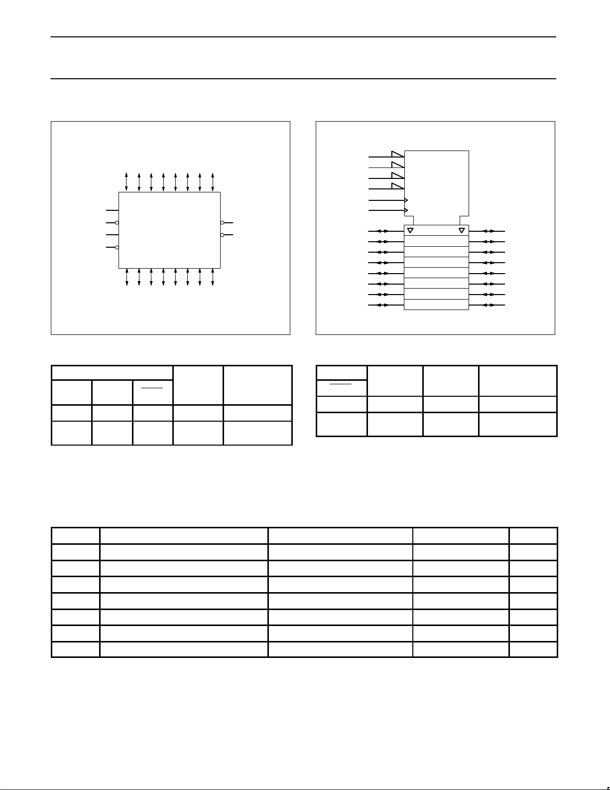
LOGIC SYMBOL
16 17 18 19 20 21 22 23
A0 A1 A2 A3 A4 A5 A6 A7
10
CPAB
11
CEAB
14
CPBA
13
CEBA
B0 B1 B2 B3 B4 B5 B6 B7
87654321
OEBA
OEAB
FUNCTION TABLE for Register An or Bn
INPUTS INTERNAL OPERATING
An or
Bn
X X H NC Hold data
L
H
H = High voltage level
L =Low voltage level
↑ =Low-to-High transition
X = Don’t care
XX=AB or BA
NC=No change
CPXX CEXX Q MODE
↑
↑
L
L
L
H
Load data
LOGIC SYMBOL (IEEE/IEC)
11
13
15
9
10
14
15
9
SA00306
16 8
17 7
18 6
19 5
20 4
21 3
22 2
23 1
EN1
EN2
EN3
EN4
C5
C6
2, 3, 6
1, 4, 5
SA00307
FUNCTION TABLE for Output Enable
INPUTS INTERNAL An or Bn OPERATING
OEXX Q OUTPUTS MODE
H X Z Disable outputs
L
L
H = High voltage level
L =Low voltage level
X = Don’t care
XX=AB or BA
Z =High impedance ”off” state
L
H
H
L
Enable outputs
ABSOLUTE MAXIMUM RATINGS
SYMBOL
V
CC
I
IK
V
I
I
OK
V
OUT
I
OUT
T
stg
DC supply voltage –0.5 to +7.0 V
DC input diode current VI < 0 –18 mA
DC input voltage
DC output diode current VO < 0 –50 mA
DC output voltage
DC output current output in Low state 128 mA
Storage temperature range –65 to 150 °C
PARAMETER CONDITIONS RATING UNIT
3
3
1, 2
–1.2 to +7.0 V
output in Off or High state –0.5 to +5.5 V
NOTES:
1. Stresses beyond those listed may cause permanent damage to the device. These are stress ratings only and functional operation of the
device at these or any other conditions beyond those indicated under “recommended operating conditions” is not implied. Exposure to
absolute-maximum-rated conditions for extended periods may affect device reliability .
2. The performance capability of a high-performance integrated circuit in conjunction with its thermal environment can create junction
temperatures which are detrimental to reliability. The maximum junction temperature of this integrated circuit should not exceed 150°C.
3. The input and output voltage ratings may be exceeded if the input and output current ratings are observed.
1995 Sep 06
2
Page 3
Philips Semiconductors Product specification
74ABT2953Octal registered transceiver, inverting (3-State)
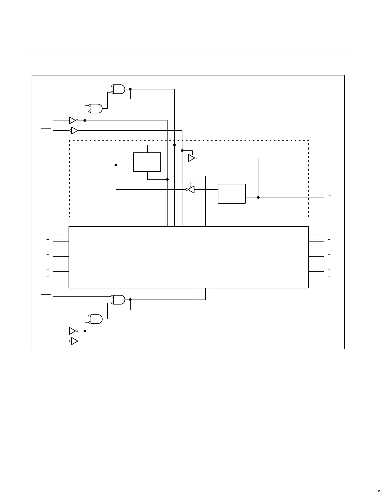
LOGIC DIAGRAM
11
CEAB
10
CPAB
9
OEAB
DETAIL A
CE
CP
Q
CE
Q
D
CP
8
B0
16
A0
D
CEBA
CPBA
OEBA
17
1
A
18
2
A
19
3
A
20
4
A
21
5
A
22
6
A
23
7
A
13
14
15
DETAIL A X 7
7
1
B
6
2
B
5
3
B
4
4
B
3
5
B
2
6
B
1
7
B
SA00308
1995 Sep 06
3
Page 4
Philips Semiconductors Product specification
74ABT2953Octal registered transceiver, inverting (3-State)
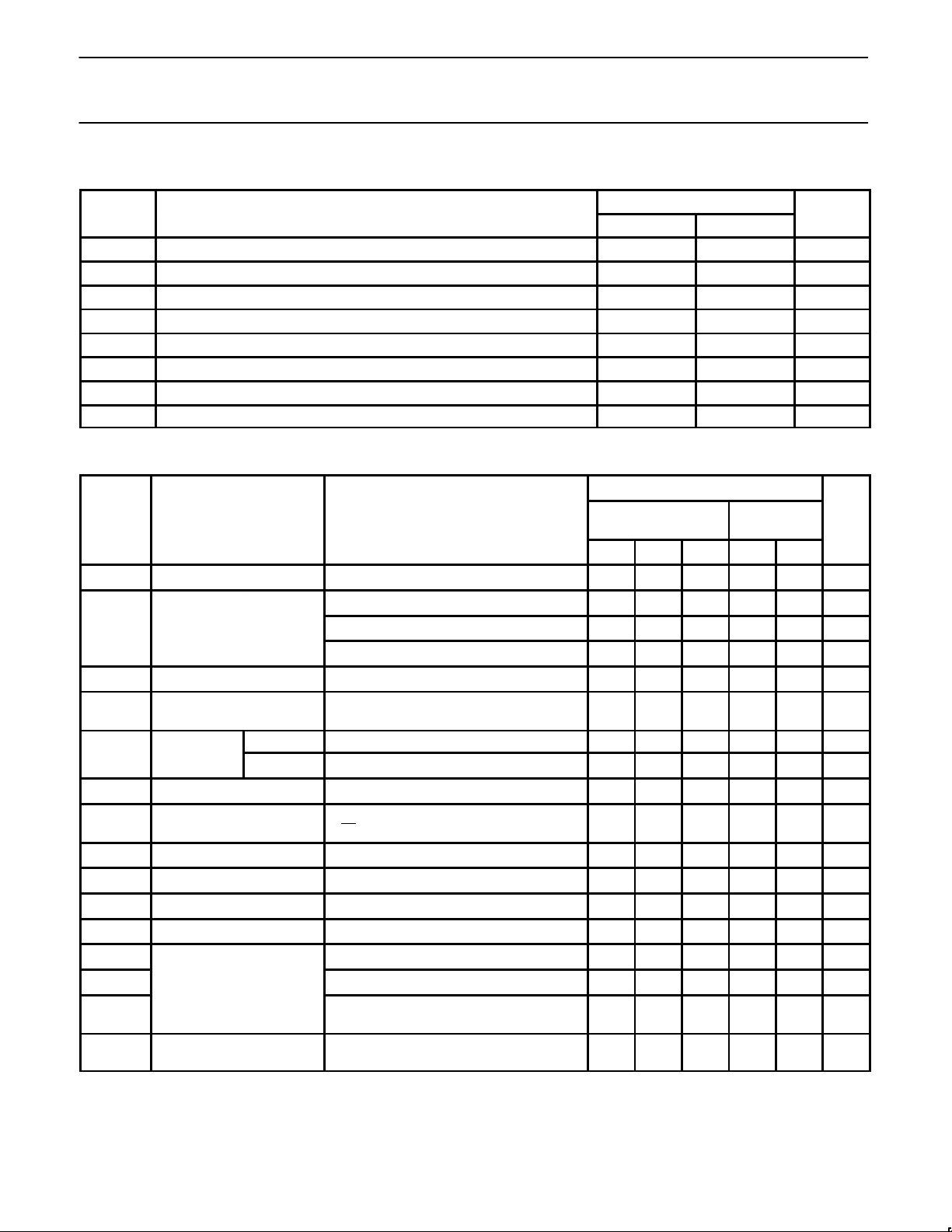
RECOMMENDED OPERATING CONDITIONS
SYMBOL PARAMETER LIMITS UNIT
Min Max
V
CC
V
V
V
I
OH
I
OL
∆t/∆v Input transition rise or fall rate 0 10 ns/V
T
amb
DC ELECTRICAL CHARACTERISTICS
SYMBOL P ARAMETER TEST CONDITIONS T
V
IK
V
OH
V
OL
V
RST
I
I
OFF
IPU/
I
OZH
I
OZL
I
CEX
I
O
I
CCH
I
CCL
I
CCZ
∆I
CC
NOTES:
1. Not more than one output should be tested at a time, and the duration of the test should not exceed one second.
2. This is the increase in supply current for each input at 3.4V.
3. For valid test results, data must not be loaded into the flip-flops (or latches) after applying the power.
4. This parameter is valid for any V
transition time of up to 100µsec is permitted.
DC supply voltage 4.5 5.5 V
Input voltage 0 V
I
High-level input voltage 2.0 V
IH
Low-level Input voltage 0.8 V
IL
CC
High-level output current –32 mA
Low-level output current 64 mA
Operating free-air temperature range –40 +85 °C
LIMITS
T
amb
= +25°C
amb
to +85°C
Min Typ Max Min Max
Input clamp voltage VCC = 4.5V; IIK = –18mA –0.9 –1.2 –1.2 V
VCC = 4.5V; IOH = –3mA; VI = VIL or V
High-level output voltage VCC = 5.0V; IOH = –3mA; VI = VIL or V
VCC = 4.5V; IOH = –32mA; VI = VIL or V
Low-level output voltage VCC = 4.5V; IOL = 64mA; VI = VIL or V
Power-up output low
3
voltage
Input leakage Control pins VCC = 5.5V; VI = GND or 5.5V ±0.01 ±1.0 ±1.0 µA
I
VCC = 5.5V; IO = 1mA; VI = GND or V
IH
IH
IH
IH
CC
2.5 3.2 2.5 V
3.0 3.7 3.0 V
2.0 2.3 2.0 V
0.42 0.55 0.55 V
0.13 0.55 0.55 V
current Data pins VCC = 5.5V; VI = GND or 5.5V ±5 ±100 ±100 µA
Power-off leakage current VCC = 0.0V; VO or VI ≤ 4.5V ±5.0 ±100 ±100 µA
Power-up/down 3-State
IPD
output current
4
3-State output High current VCC = 5.5V; VO = 2.7V; VI = VIL or V
3-State output Low current VCC = 5.5V; VO = 0.5V; VI = VIL or V
Output High leakage current VCC = 5.5V; VO = 5.5V; VI = GND or V
Output current
1
Quiescent supply current VCC = 5.5V; Outputs Low, VI = GND or V
Additional supply current per
input pin
2
CC
VCC = 2.1V; VO = 0.5V; VI = GND or VCC;
= Don’t care
V
OE
IH
IH
CC
±5.0 ±50 ±50 µA
5.0 50 50 µA
–5.0 –50 –50 µA
5.0 50 50 µA
VCC = 5.5V; VO = 2.5V –50 –65 –180 –50 –180 mA
VCC = 5.5V; Outputs High, VI = GND or V
VCC = 5.5V; Outputs 3-State;
= GND or V
V
I
CC
VCC = 5.5V; one input at 3.4V,
other inputs at V
or GND
CC
CC
CC
110 250 250 µA
20 30 30 mA
110 250 250 µA
0.3 1.5 1.5 mA
between 0V and 2.1V, with a transition time of up to 10msec. From VCC = 2.1V to VCC = 5V ± 10% a
= –40°C
V
UNIT
1995 Sep 06
4
Page 5
Philips Semiconductors Product specification
74ABT2953Octal registered transceiver, inverting (3-State)
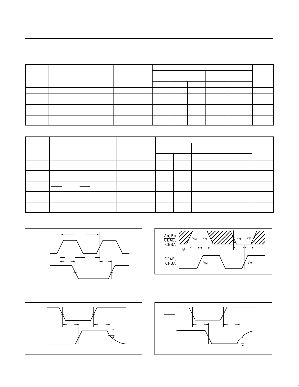
AC CHARACTERISTICS
GND = 0V; tR = tF = 2.5ns; CL = 50pF, RL = 500Ω
LIMITS
T
SYMBOL PARAMETER WAVEFORM
f
MAX
t
PLH
t
PHL
t
PZH
t
PZL
t
PHZ
t
PLZ
Maximum clock frequency 1 150 200 150 MHz
Propagation delay
CPBA to An, CPAB to Bn
Output enable time
OEBA to An, OEAB to Bn
Output disable time
OEBA to An, OEAB to Bn
1
3
4
3
4
AC SETUP REQUIREMENTS
SYMBOL PARAMETER WAVEFORM
tS(H)
(L)
t
s
th(H)
(L)
t
h
ts(H)
(L)
t
s
th(H)
(L)
t
h
tw(H)
(L)
t
w
Setup time
An to CPAB or Bn to CPBA
Hold time
An to CPAB or Bn to CPBA
Setup time
to CPAB, CEBA to CPBA
CEAB
Hold time
to CPAB, CEBA to CPBA
CEAB
CPAB or CPBA pulse width,
High or Low
2
2
2
2
1
= +25°C
amb
= +5.0V
V
CC
Min Typ Max Min Max
2.0
2.5
1.0
2.2
2.0
1.5
T
V
amb
= +25°C
= +5.0V
CC
5.1
5.7
4.0
5.3
6.1
5.6
Min Typ Min
4.0
3.0
0.0
0.0
3.5
2.5
0.0
0.0
3.0
3.5
2.5
1.1
–1.0
–2.0
2.0
0.9
–0.5
–1.0
2.0
1.1
6.6
7.2
4.8
6.2
7.6
7.1
LIMITS
T
= –40°C to +85°C
amb
= +5.0V ±0.5V
V
CC
2.0
2.5
1.0
2.2
2.0
1.5
T
= –40°C to +85°C
amb
= +5.0V ±0.5V
V
CC
4.0
3.0
0.0
0.0
3.5
2.5
0.0
0.0
3.0
3.5
7.6
8.2
5.8
7.5
8.1
7.6
UNIT
ns
ns
ns
UNIT
ns
ns
ns
ns
ns
AC WAVEFORMS
VM = 1.5V, VIN = GND to 3.0V
1/f
MAX
CPBA or
CPAB
An or Bn
Waveform 1. Propagation Delay, Clock Input to Output, Clock
Pulse Width, and Maximum Clock Frequency
OEAB,
OEBA
An, Bn
Waveform 3. 3-State Output Enable Time to High Level and
V
M
tw(H) tw(L)
t
PHL
V
M
t
PZH
V
M
V
M
V
V
M
V
M
t
PLH
M
t
PHZ
Output Disable Time from High Level
V
M
SA00087
–0.3V
V
OH
0V
SA00310
An, Bn
CEAB
V
V
M
,
M
V
V
M
M
CEBA
t
(L)
(H)
t
s
h
(L)
t
h
V
M
SA00309
CPAB,
CPBA
ts(H)
V
M
Waveform 2. Data Setup and Hold Times
OEAB,
OEBA
An, Bn
V
M
t
PZL
V
M
t
PLZ
V
M
V
OL
+0.3V
0V
SA00311
Waveform 4. 3-State Output Enable Time to Low Level and
Output Disable Time from Low Level
1995 Sep 06
5
Page 6
Philips Semiconductors Product specification
74ABT2953Octal registered transceiver, inverting (3-State)
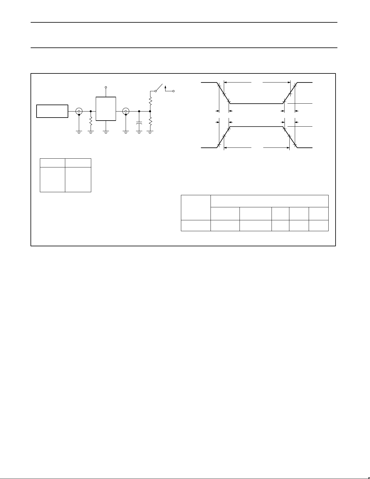
TEST CIRCUIT AND WAVEFORMS
V
CC
R
PULSE
GENERATOR
V
IN
R
D.U.T.
T
V
OUT
C
L
L
R
L
Test Circuit for 3-State Outputs
SWITCH POSITION
TEST SWITCH
t
PLZ
t
PZL
closed
closed
All other open
DEFINITIONS
RL = Load resistor; see AC CHARACTERISTICS for value.
= Load capacitance includes jig and probe capacitance;
C
L
see AC CHARACTERISTICS for value.
= Termination resistance should be equal to Z
R
T
pulse generators.
OUT
of
t
W
(tF)
(tR)t
t
W
90%
V
M
V
M
10%
7.0V
90%
NEGATIVE
PULSE
POSITIVE
PULSE
10%
V
M
10% 10%
t
THL
t
TLH
90% 90%
V
M
VM = 1.5V
Input Pulse Definition
INPUT PULSE REQUIREMENTS
FAMILY
Amplitude Rep. Rate t
t
W
74ABT 3.0V 1MHz 500ns 2.5ns 2.5ns
AMP (V)
0V
t
(tR)
TLH
(tF)
THL
AMP (V)
0V
t
R
F
SA00012
1995 Sep 06
6
 Loading...