

Page 1
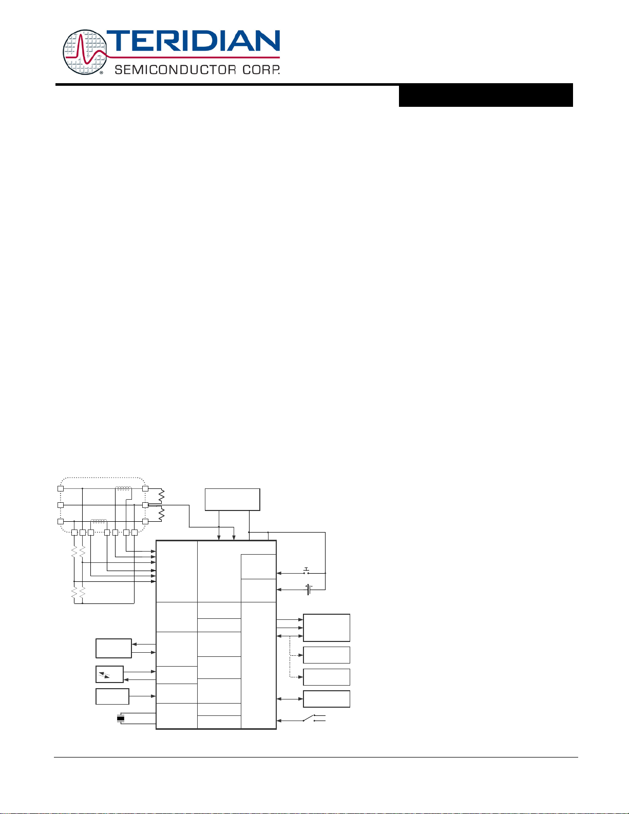
71M6531D/F, 71M6532D/F
Energy Meter IC
MPU
TIMERS
IAP*
VA
IBP*
XIN
XOUT
VREF
RX/DIO1
TX/DIO2
V1
TX
RX
COM0..3
V3.3A
V3.3
SYS
VBAT
V2.5
VBIAS
GNDA GNDD
SEG/DIO
ICE I/F
LOAD
88. 88.8888
I2C or µWire
EEPROM
POWER
FAULT
AMR
TEST PULSES
COMPARATOR
SENSE
DRIVE/MOD
SERIAL PORTS
OSC/PLL
ADC
LCD & DIO
COMPUTE
ENGINE
FLASH
MEMORY
RAM
VOLTAGE REF
REGULATOR
POWER SUPPLY
TERIDIAN
71M6531
71M6532
TEMP
SENSOR
32 kHz
A
NEUTRAL
CT/SHUNT
02/18/2009
VB
B
LOAD
IR
PWR MODE
CONTROL
WAKE-UP
BATTERY
ICE_E GNDD
V3P3D
IAN*
IBN*
CT
SPI HOST
SPI
LCD SEG
RTC
*
Differential pins only on 6532D/F
Simplifying System Integration
TM
DATA SHEET
June 2010
GENERAL DESCRIPTION
The Teridian 71M6531D/F and 71M6532D/F are highly
integrated SOCs with an MPU core, RTC, FLASH and LCD
driver. Teridian’s patented Single Converter Technology®
with a 22-bit delta-sigma ADC, four ana log inputs, digital
temperature compe nsation, precisio n voltage r eference, battery
voltage monitor and 32-bit computation engine (CE) supports
a wide range of residential metering applications with very few
low-cost external components.
A 32-kHz crystal time base for the entire system and internal
battery backup support for RAM and RTC further reduce system
cost. The IC suppor ts 2-wire, and 3-wire single-phase and
dual-phase residential metering along with t am per-detection
mechanisms. The 71M6531D/F offers single-ended inputs for
two current channels and two single-ended voltage inputs.
The 71M6532D/F has two differential current inputs and three
single-ended voltage inputs.
2
Maximum design flexibility is provided by multiple UARTs, I
μWire, up to 21 DIO pins and in-system programmable FLASH
memory, which can be updated with data or application code
in operation.
A complete array of ICE and development t ool s, programming
libraries and reference designs enable rapid development and
certification of TOU, AMR and Prepay meters that comply with
worldwide electricity metering standards.
C,
FEATURES
• Wh accuracy < 0.1% over 2000:1 current
range
• Exceeds IEC62053/ANSI C12.20 standards
• Four sensor inputs
• Low-jitter Wh and VARh plus two additional
pulse test outputs (4 total, 10 kHz maximum)
with pulse count
• Four-quadrant metering
• Tamper detection (Neutral current with CT,
Rogowski or shunt, magnetic tamper input)
• Line frequency count for RTC
• Digital temperature compensation
• Sag detection for phase A and B
• Independent 32-bit compute engine
• 46-64 Hz line frequency range with same
calibration. Phase compensation (± 7°)
• Three battery modes with wake-up on timer
or push-button:
Brownout mode (52 µA typ.)
LCD mode (21 µA typ., DAC active)
Sleep mode (0.7 µA typ.)
• Energy display during mains power failure
• 39 mW typical consumption @ 3.3 V, MPU
clock frequency 614 kHz
• 22-bit delta-sigma ADC with 3360 Hz or
2520 Hz sample rate
• 8-bit MPU (80515),1 clock cycle per instruction,
10 MHz maximum, with integrated ICE for
debug
• RTC for TOU functions with clock-rate adjust
register
• Hardware watchdog timer, power fail monitor
• LCD driver with 4 common segment drivers:
Up to 156 (71M6531D/F) or 268 pixels
(71M6532D/F)
• Up to 22 (71M6531D/F) or 43 (71M6532D/F)
general-purpose I/O pins. Digital I/O pins
compatible with 5 V inputs
• 32 kHz time base
v1.3 © 2005-2010 TERIDIAN Semiconductor Corporation 1
• High-speed slave SPI interface t o data RAM
• Two UARTs for IR and AMR, IR driver with
modulation
• FLASH memory with security and in-system
program update:
128 KB (71M6531D/32D)
256 KB (71M6531F/32F)
• 4 KB MPU XRAM
• Industrial temperature range
• 68-pin QFN package for 71M6531D/F pin-
compatible with 71M6521, 100-pin LQFP
package for 71M6532D/F, lead free
Page 2

Data Sheet 71M6531D/F-71M6532D/F FDS 6531/6532 005
Table of Contents
1 Hardware Description ....................................................................................................................... 10
1.1 Hardware Overview ................................................................................................................... 10
1.2 Analog Front End (AFE) ............................................................................................................. 10
1.2.1 Signal Input Pins ............................................................................................................ 10
1.2.2 Input Multiplexer ............................................................................................................ 11
1.2.3 A/D Converter (ADC) ..................................................................................................... 12
1.2.4 FIR Filter ........................................................................................................................ 12
1.2.5 Voltage References ....................................................................................................... 12
1.2.6 Temperature Sensor ...................................................................................................... 14
1.2.7 Battery Monitor............................................................................................................... 14
1.2.8 AFE Functional Description ........................................................................................... 14
1.2.9 Digital Computation Engine (CE) ................................................................................... 15
1.2.10 Meter Equations ............................................................................................................. 16
1.2.11 Real-Time Monitor ......................................................................................................... 16
1.2.12 Pulse Generators ........................................................................................................... 16
1.2.13 Data RAM (XRAM) ........................................................................................................ 17
1.2.14 Delay Compensation ..................................................................................................... 17
1.2.15 CE Functional Overview ................................................................................................ 17
1.3 80515 MPU Core ....................................................................................................................... 19
1.3.1 Memory Organization and Addressing .......................................................................... 19
1.3.2 Special Function Registers (SFRs) ............................................................................... 21
1.3.3 Generic 80515 Special Function Registers ................................................................... 22
1.3.4 Special Function Registers (SFRs) Specific t o the 71M6531D/F and 71M6532D/F ..... 24
1.3.5 Instruction Set ................................................................................................................ 26
1.3.6 UARTs ........................................................................................................................... 26
1.3.7 Timers and Counters ..................................................................................................... 28
1.3.8 WD Timer (Software Watchdog Timer) ......................................................................... 30
1.3.9 Interrupts ........................................................................................................................ 30
1.4 On-Chip Resources ................................................................................................................... 36
1.4.1 Oscillator ........................................................................................................................ 36
1.4.2 Internal Clocks ............................................................................................................... 36
1.4.3 Real-Time Clock (RTC) ................................................................................................. 37
1.4.4 Temperature Sensor ...................................................................................................... 38
1.4.5 Physical Memory............................................................................................................ 38
1.4.6 Optical Interface ............................................................................................................. 40
1.4.7 Digital I/O – 71M6531D/F .............................................................................................. 41
1.4.8 Digital I/O – 71M6532D/F .............................................................................................. 43
1.4.9 Digital IO – Common Characteristics for 71M6531D/F and 71M 6532D/F .................... 44
1.4.10 LCD Drivers – 71M6531D/F .......................................................................................... 45
1.4.11 LCD Drivers – 71M6532D/F .......................................................................................... 46
1.4.12 LCD Drivers – Common Characteristics for 71M6531D/ F and 71M6532D/F ............... 46
1.4.13 Battery Monitor............................................................................................................... 46
1.4.14 EEPROM Interface ........................................................................................................ 46
1.4.15 SPI Slave Port................................................................................................................ 49
1.4.16 Hardware Watchdog Timer ............................................................................................ 52
1.4.17 Test Ports (TMUXOUT pin) ........................................................................................... 53
2 © 2005-2010 TERIDIAN Semiconductor Corporation v1.3
Page 3

FDS 6531/6532 005 Data Sheet 71M6531D/F-71M6532D/F
2 Functional Description ..................................................................................................................... 54
2.1 Theory of Operation ................................................................................................................... 54
2.2 System Timing Summary ........................................................................................................... 55
2.3 Battery Modes ............................................................................................................................ 56
2.3.1 BROWNOUT Mode ....................................................................................................... 57
2.3.2 LCD Mode ...................................................................................................................... 58
2.3.3 SLEEP Mode ................................................................................................................. 58
2.4 Fault and Reset Behavior .......................................................................................................... 60
2.4.1 Reset Mode .................................................................................................................... 60
2.4.2 Power Fault Circuit ........................................................................................................ 60
2.5 Wake-Up Behavior ..................................................................................................................... 61
2.5.1 Wake on PB ................................................................................................................... 61
2.5.2 Wake on Timer............................................................................................................... 61
2.6 Data Flow ................................................................................................................................... 61
2.7 CE/MPU Communication ........................................................................................................... 62
3 Application Information .................................................................................................................... 63
3.1 Connection of Sensors ............................................................................................................... 63
3.2 Connecting 5-V Devices ............................................................................................................ 63
3.3 Temperature Measurement ....................................................................................................... 64
3.4 Temperature Compensation ...................................................................................................... 64
3.4.1 Temperature Coefficients: ............................................................................................. 64
3.4.2 Temperature Compensation for VREF .......................................................................... 65
3.4.3 System Temperature Compensation ............................................................................. 65
3.4.4 Temperature Compensation for the RTC ...................................................................... 65
3.5 Connecting LCDs ....................................................................................................................... 66
3.6 Connecting I2C EEPROMs ........................................................................................................ 66
3.7 Connecting Three-Wire EEPROMs ........................................................................................... 67
3.8 UART0 (TX/RX) ......................................................................................................................... 67
3.9 Optical Interface (UART1) .......................................................................................................... 67
3.10 Connecting the V1 Pin ............................................................................................................... 68
3.11 Connecting the Reset Pin .......................................................................................................... 69
3.12 Connecting the Emulator Port Pins ............................................................................................ 69
3.13 Connecting a Battery ................................................................................................................. 69
3.14 Flash Programming .................................................................................................................... 70
3.15 MPU Firmware ........................................................................................................................... 70
3.16 Crystal Oscillator ........................................................................................................................ 70
3.17 Meter Calibration ........................................................................................................................ 71
4 Firmware Interface ............................................................................................................................ 72
4.1 I/O RAM and SFR Map – Functional Order ............................................................................... 72
4.2 I/O RAM Description – Alphabetical Order ................................................................................ 77
4.3 CE Interface Description ............................................................................................................ 88
4.3.1 CE Program ................................................................................................................... 88
4.3.2 CE Data Format ............................................................................................................. 88
4.3.3 Constants ....................................................................................................................... 88
4.3.4 Environment ................................................................................................................... 88
4.3.5 CE Calculations ............................................................................................................. 89
4.3.6 CE Status and Control ................................................................................................... 89
4.3.7 CE Transfer Variables ................................................................................................... 92
4.3.8 Pulse Generation ........................................................................................................... 93
4.3.9 CE Calibration Parameters ............................................................................................ 94
v1.3 © 2005-2010 TERIDIAN Semiconductor Corporation 3
Page 4

Data Sheet 71M6531D/F-71M6532D/F FDS 6531/6532 005
4.3.10 Other CE Parameters .................................................................................................... 95
4.3.11 CE Flow Diagrams ......................................................................................................... 95
5 Electrical Specifications ................................................................................................................... 98
5.1 Absolute Maximum Ratings ....................................................................................................... 98
5.2 Recommended External Components ....................................................................................... 99
5.3 Recommended Operating Conditions ........................................................................................ 99
5.4 Performance Specifications ..................................................................................................... 100
5.4.1 Input Logic Levels ........................................................................................................ 100
5.4.2 Output Logic Levels ..................................................................................................... 100
5.4.3 Power-Fault Comparator ............................................................................................. 100
5.4.4 Battery Monitor............................................................................................................. 100
5.4.5 Supply Current ............................................................................................................. 101
5.4.6 V3P3D Switch .............................................................................................................. 101
5.4.7 2.5 V Voltage Regulator ............................................................................................... 101
5.4.8 Low-Power Voltage Regulator ..................................................................................... 101
5.4.9 Crystal Oscillator .......................................................................................................... 102
5.4.10 LCD DAC ..................................................................................................................... 102
5.4.11 LCD Drivers ................................................................................................................. 102
5.4.12 Optical Interface ........................................................................................................... 102
5.4.13 Temperature Sensor .................................................................................................... 103
5.4.14 VREF ........................................................................................................................... 103
5.4.15 ADC Converter, V3P3A Referenced ........................................................................... 104
5.5 Timing Specifications ............................................................................................................... 105
5.5.1 Flash Memory .............................................................................................................. 105
5.5.2 EEPROM Interface ...................................................................................................... 105
5.5.3 RESET ......................................................................................................................... 105
5.5.4 RTC .............................................................................................................................. 105
5.5.5 SPI Slave Port (MISSION Mode) ................................................................................. 106
5.6 Typical Performance Data ....................................................................................................... 107
5.6.1 Accuracy over Current ................................................................................................. 107
5.6.2 Accuracy over Temperature ........................................................................................ 107
5.7 71M6531D/F Package ............................................................................................................. 108
5.7.1 Package Outline .......................................................................................................... 108
5.7.2 71M6531D/F Pinout (QFN-68) ..................................................................................... 109
5.7.3 Recommended PCB Land Pattern for the QFN-68 Package ...................................... 110
5.8 71M6532D/F Package ............................................................................................................. 111
5.8.1 71M6532D/F Pinout (LQFP-100) ................................................................................. 111
5.8.2 LQFP-100 Mechanical Drawing ................................................................................... 112
5.9 Pin Descriptions ....................................................................................................................... 113
5.9.1 Power and Ground Pins ............................................................................................... 113
5.9.2 Analog Pins .................................................................................................................. 113
5.9.3 Digital Pins ................................................................................................................... 114
5.9.4 I/O Equivalent Circuits ................................................................................................. 115
6 Ordering Information ...................................................................................................................... 116
7 Related Information ........................................................................................................................ 116
8 Contact Information ........................................................................................................................ 116
Appendix A: Acronyms .......................................................................................................................... 117
Appendix B: Revision History ............................................................................................................... 118
4 © 2005-2010 TERIDIAN Semiconductor Corporation v1.3
Page 5

FDS 6531/6532 005 Data Sheet 71M6531D/F-71M6532D/F
Figures
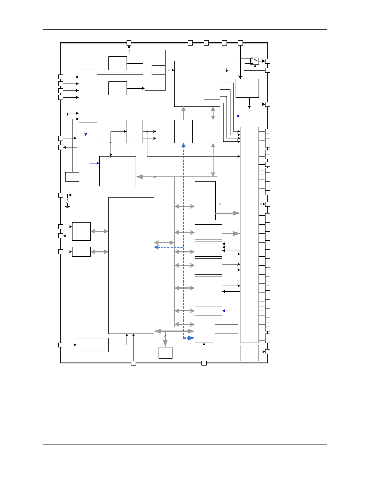
Figure 1: 71M6531D/F IC Functional Block Diagram ................................................................................... 8
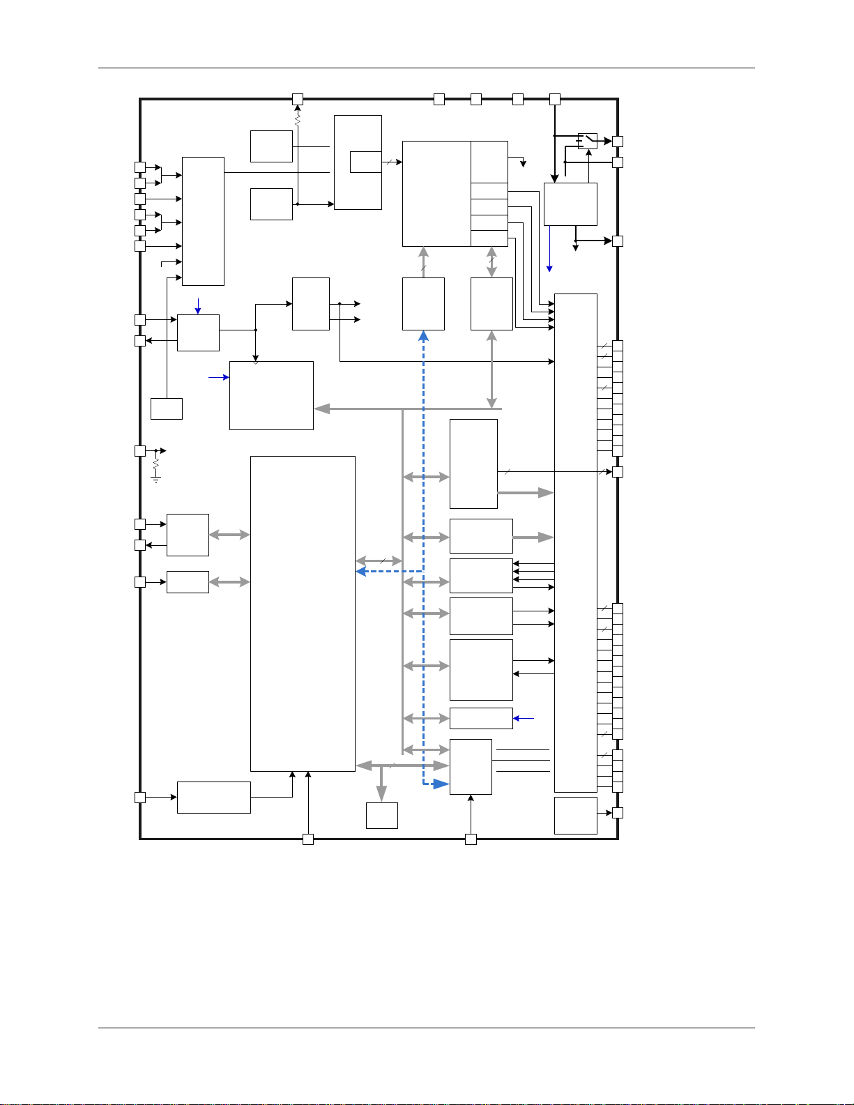
Figure 2: 71M6532D/F IC Functional Block Diagram ................................................................................... 9
Figure 3: General Topology of a Chopped Ampli fier .................................................................................. 13
Figure 4: CROSS Signal with CHOP_E[1:0] = 00 ....................................................................................... 13
Figure 5: AFE Block Diagram (Shown for the 71M65 32D/F) ...................................................................... 14
Figure 6: Samples from Multiplexer Cyc le .................................................................................................. 18
Figure 7: Accumulation Interval .................................................................................................................. 18
Figure 8: Interrupt Structure ........................................................................................................................ 35
Figure 9: Optical Interface ........................................................................................................................... 41
Figure 10: Connecting an External Load to DIO Pins ................................................................................. 45
Figure 11: 3-Wire Interface. Write Command, HiZ =0 ................................................................................ 48
Figure 12: 3-Wire Interface. Write Command, HiZ =1 ................................................................................ 48
Figure 13: 3-Wire Interface. Read Command. ........................................................................................... 49
Figure 14: 3-Wire Interface. Write Command when CNT=0 ...................................................................... 49
Figure 15: 3-Wire Interface. Write Command when HiZ =1 and WFR=1 ................................................... 49
Figure 16: SPI Slave Port: Typical Read and Write operations .................................................................. 51
Figure 17: Functions defined by V1 ............................................................................................................ 52
Figure 18: Voltage, Current, Momentary and Ac cumulated Energy ........................................................... 54
Figure 19: Timing Relationship between ADC MUX, Compute Engine ...................................................... 55
Figure 20: RTM Output Format ................................................................................................................... 55
Figure 21: Operation Modes State Diagram ............................................................................................... 56
Figure 22: Transition from BROWNOUT t o M ISSION Mode when System Power Returns ...................... 59
Figure 23: Power-Up Timing with V3P3SYS and VBAT tied together ........................................................ 59
Figure 24: Power-Up Timing with VBAT only .............................................................................................. 60
Figure 25: Wake Up Timing ........................................................................................................................ 61
Figure 26: MPU/CE Data Flow .................................................................................................................... 62
Figure 27: MPU/CE Communication ........................................................................................................... 62
Figure 28: Resistive Voltage Divider ........................................................................................................... 63
Figure 29: CT with Single Ended (Left) and Diff erential Input (Right) Connection ..................................... 63
Figure 30: Resistive Shunt (Left) and Rogowski Sensor (Right) Connection ............................................. 63
Figure 31: Connecting LCDs ....................................................................................................................... 66
Figure 32: I2C EEPROM Connection .......................................................................................................... 66
Figure 33: Three-Wire EEPROM Connection ............................................................................................. 67
Figure 34: Connections for UART0 ............................................................................................................. 67
Figure 35: Connection for Optical Component s .......................................................................................... 68
Figure 36: Voltage Divider for V1 ................................................................................................................ 68
Figure 37: External Components for the RES E T Pin: Push-button (Left), Production Circuit (Right) ........ 69
Figure 38: External Components for the Em ulator Interface ...................................................................... 69
Figure 39: Connecting a Battery ................................................................................................................. 70
Figure 40: CE Data Flow: Multiplexer and ADC.......................................................................................... 96
Figure 41: CE Data Flow: Scaling, Gain Control, Intermediate Variables .................................................. 96
Figure 42: CE Data Flow: Squaring and Sum m ation Stages ...................................................................... 97
Figure 43: SPI Slave Port (MISSION Mode) Timing ................................................................................. 106
Figure 44: Wh Accuracy, 0.1 A to 200 A at 240 V/50 H z and Room Temperature .................................. 107
Figure 45: QFN-68 Package Outline, Top and Side View ........................................................................ 108
Figure 46: QFN-68 Package Outline, Bottom Vi ew .................................................................................. 108
Figure 47: Pinout for QFN-68 Package ..................................................................................................... 109
Figure 48: PCB Land Pattern for QFN 68 Package .................................................................................. 110
Figure 49: PCB Land Pattern for LQFP-100 Package .............................................................................. 111
Figure 50: LQFP-100 Package, Mechanical Dra wing ............................................................................... 112
Figure 51: I/O Equivalent Circuits ............................................................................................................. 115
v1.3 © 2005-2010 TERIDIAN Semiconductor Corporation 5
Page 6

Data Sheet 71M6531D/F-71M6532D/F FDS 6531/6532 005
Tables
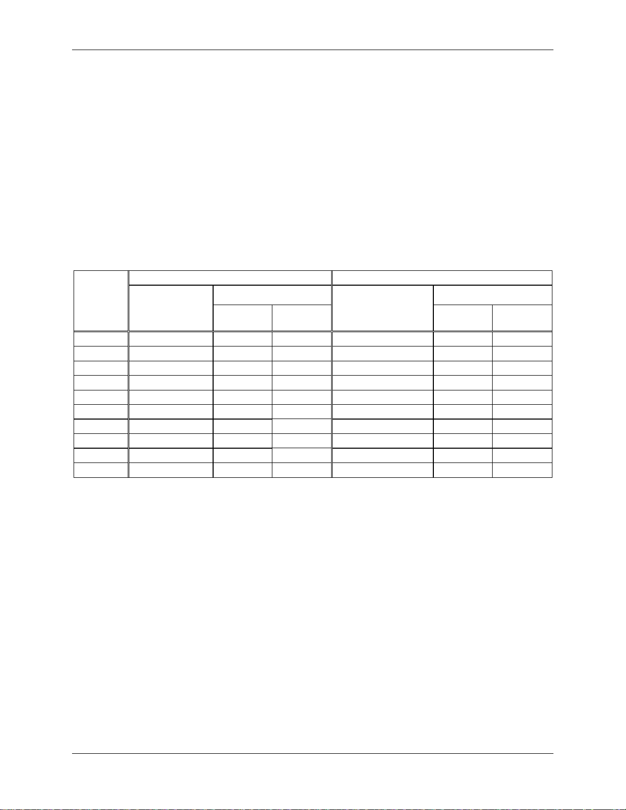
Table 1: Inputs Selected in Regular and Alternat e M ultiplexer Cycles ....................................................... 11
Table 2: ADC Resolution ............................................................................................................................. 12
Table 3: ADC RAM Locations ..................................................................................................................... 12
Table 4: XRAM Locations for ADC Results ................................................................................................ 15
Table 5: Meter Equations ............................................................................................................................ 16
Table 6: CKMPU Clock Frequencies .......................................................................................................... 19
Table 7: Memory Map ................................................................................................................................. 20
Table 8: Internal Data Memory Map ........................................................................................................... 21
Table 9: Special Function Register Map ..................................................................................................... 21
Table 10: Generic 80515 SFRs - Location and Reset Values .................................................................... 22
Table 11: PSW Bit Functions (SFR 0xD0) ..................................................................................................... 23
Table 12: Port Registers ............................................................................................................................. 24
Table 13: Stretch Memory Cycle Width ...................................................................................................... 24
Table 14: 71M6531D/F and 71M6532D/F Specific SF Rs ........................................................................... 24
Table 15: Baud Rate Generation ................................................................................................................ 26
Table 16: UART Modes ............................................................................................................................... 26
Table 17: The S0CON (UART0) Register (SFR 0x98) ................................................................................. 27
Table 18: The S1CON (UART1) register (SFR 0x9B) .................................................................................. 27
Table 19: PCON Register Bit Description (SFR 0x87) ................................................................................ 28
Table 20: Timers/Counters Mode Description ............................................................................................ 28
Table 21: Allowed Timer/Counter Mode Combinations .............................................................................. 29
Table 22: TMOD Register Bit Description (SFR 0x89) ................................................................................ 29
Table 23: The TCON Register Bit Functions (SF R 0x 88) ............................................................................ 29
Table 24: The IEN0 Bit Functions (SFR 0xA8) ............................................................................................ 30
Table 25: The IEN1 Bit Functions (SFR 0xB8) ............................................................................................ 31
Table 26: The IEN2 Bit Functions (SFR 0x9A) ............................................................................................ 31
Table 27: TCON Bit Functions (SFR 0x88) ................................................................................................. 31
Table 28: The T2CON Bit Functions (SFR 0xC8) ........................................................................................ 31
Table 29: The IRCON Bit Functions (SFR 0xC0) ........................................................................................ 31
Table 30: External MPU Interrupts .............................................................................................................. 32
Table 31: Interrupt Enable and Flag Bits .................................................................................................... 32
Table 32: Interrupt Priority Level Groups .................................................................................................... 33
Table 33: Interrupt Priority Levels ............................................................................................................... 33
Table 34: Interrupt Priority Registers (IP0 and IP1) .................................................................................... 34
Table 35: Interrupt Polling Sequence .......................................................................................................... 34
Table 36: Interrupt Vectors .......................................................................................................................... 34
Table 37: Clock System Summary .............................................................................................................. 36
Table 38: Bank Switching with FL_BANK[2:0] ............................................................................................ 40
Table 39: Data/Direction Registers and Internal Resources for DIO 1-15 (71M6531D/F) ......................... 42
Table 40: Data/Direction Registers and Internal Resources for DIO 17-29 (71M6531D/F) ....................... 42
Table 41: Data/Direction Registers and Internal Resources for DIO 43-46 (71M6531D/F) ....................... 42
Table 42: Data/Direction Registers and Internal Resources for DIO 1-15 (71M6532D/F) ......................... 43
Table 43: Data/Direction Registers and Internal Resources for DIO 16-30 (71M6532D/F) ....................... 43
Table 44: Data/Direction Registers and Internal Resources for DIO 40-51 (71M6532D/F) ....................... 44
Table 45: DIO_DIR Control Bit .................................................................................................................... 44
Table 46: Selectable Control using DIO_DIR Bits ......................................................................................... 44
Table 47: EECTRL Bits for 2-pin Interface ................................................................................................... 47
Table 48: EECTRL Bits for the 3-Wire Interface .......................................................................................... 48
Table 49: SPI Command Description .......................................................................................................... 50
Table 50: I/O RAM Registers Accessible via S P I ....................................................................................... 50
Table 51: TMUX[4:0] Selections ................................................................................................................. 53
Table 52: Available Circuit Functions .......................................................................................................... 57
6 © 2005-2010 TERIDIAN Semiconductor Corporation v1.3
Page 7

FDS 6531/6532 005 Data Sheet 71M6531D/F-71M6532D/F
Table 53: I/O RAM Map in Functional Order ............................................................................................... 72
Table 54: I/O RAM Description - Alphabetical ............................................................................................ 77
Table 55: CE EQU[2:0] Equations and Element Input Mapping ................................................................. 89
Table 56: CESTATUS (CE RAM 0x80) Bit Definitions .................................................................................. 90
Table 57: CECONFIG Bit Definitions ........................................................................................................... 91
Table 58: Sag Threshold Control ................................................................................................................ 91
Table 59: Gain Adjust Control ..................................................................................................................... 91
Table 60: CE Transfer Variables ................................................................................................................. 92
Table 61: CE Energy Measurement Variables ............................................................................................ 92
Table 62: Useful CE Measurement Parameter s ......................................................................................... 93
Table 63: CE Pulse Generation Parameters ............................................................................................... 94
Table 64: CE Calibration Parameters ......................................................................................................... 94
Table 65: CE Parameters for Noise Suppressi on and Code Version ......................................................... 95
Table 66: Absolute Maximum Ratings ........................................................................................................ 98
Table 67: Recommended External Components ........................................................................................ 99
Table 68: Recommended Operating Condit ions ......................................................................................... 99
Table 69: Input Logic Levels ..................................................................................................................... 100
Table 70: Output Logic Levels .................................................................................................................. 100
Table 71: Power-Fault Comparator Performa nce Specifications ............................................................. 100
Table 72: Battery Monitor Performance Specifications (BME= 1) ............................................................. 100
Table 73: Supply Current Performance Specif i cations ............................................................................. 101
Table 74: V3P3D Switch Performance Specifi cat i ons .............................................................................. 101
Table 75: 2.5 V Voltage Regulator Performance Specifications ............................................................... 101
Table 76: Low-Power Voltage Regulator Performance Specifications ..................................................... 101
Table 77: Crystal Oscillator Performance Specifications .......................................................................... 102
Table 78: LCD DAC Performance Specifications ..................................................................................... 102
Table 79: LCD Driver Performance Specificat i ons ................................................................................... 102
Table 80: Optical Interface Performance Specifications ........................................................................... 102
Table 81: Temperature Sensor Performance Specifications .................................................................... 103
Table 82: VREF Performance Specifications ............................................................................................ 103
Table 83: ADC Converter Performance Specific ations ............................................................................. 104
Table 84: Flash Memory Timing Specifications ........................................................................................ 105
Table 85: EEPROM Interface Timing ........................................................................................................ 105
Table 86: RESET Timing .......................................................................................................................... 105
Table 87: SPI Slave Port (MISSION Mode) Timing .................................................................................. 106
Table 88: Recommended PCB Land Pattern Dimensions ........................................................................ 110
Table 89: Power and Ground Pins ............................................................................................................ 113
Table 90: Analog Pins ............................................................................................................................... 113
Table 91: Digital Pins ................................................................................................................................ 114
v1.3 © 2005-2010 TERIDIAN Semiconductor Corporation 7
Page 8
Data Sheet 71M6531D/F-71M6532D/F FDS 6531/6532 005
∆Σ ADC
CONVERTER
VREF
ADC_E
MUX
XIN
XOUT
VREF
DIO1/OPT_RX
RESET
V1
UART2--OPTICAL
UART1
TX
RX
4
COM0...3
LCD DISPLAY
DRIVER
DIGITAL I/O
RTCLK (32KHz)
CE_E
RTM_E
POWER FAULT
LCD_E
LCD_CLK
LCD_MODE
DIO
GNDD V3P3A
V3P3D
VBAT
VOLT
REG
2.5V to logic
V2P5
SUM_CYCLES
PRE_SAMPS
EQU
TMUXOUT
FAULTZ
TMUX[4:0]
GNDA
VBIAS
OSC
(32KHz)
MCK
PLL
VREF
VREF_DIS
TEST
TEST
MODE
DIO_R
DIO_DIR
E_RXTX
OPT_TXE
RTC
VBIAS
ICE_E
VREF_CAL
RTM_0..3
CE_LCTN
PLS_MAXWIDTH
PLS_INTERVAL
PLS_INV
OPT_TXINV
OPT_TXMOD
OPT_FDC
OPT_RXINV
OPT_RXDIS
LCD_BLKMAP
LCD_SEG
LCD_Y
SLEEP
LCD_ONLY
V3P3SYS
TEST
MUX
VBAT
CE_PROG
CK_CE
CK_MPU
VADC
CE
MULTI-
PURPOSE
IO
MUX_DIV
MUX_ALT
EQU
RTM
RPULSE
WPULSE
COM0..3
SEG...
DIO...
to TMUX
SPI SLAVE
PCMD
EEPROM
EECTRL
FLASH
128KB/
256KB
XRAM
4kB
CE_DATA
PCSZ
PCLK
PSI
PSO
SDATA
SCLK
EEDATA
OPT_TX
OPT_RX
PB
PB
IRAM
256B
MPU
EMULATOR
(ICE)
E_TCLK
E_RSTZ
DIO2/OPT_TX/WPULSE/RPULSE
SEG7/MUX_SYNC
SEG8
SEG9/E_RXTX
SEG10/E_TCLK
SEG11/E_RST
SEG12
SEG13
SEG14
SEG16
SEG15
SEG17
DIO4/SEG24/SDCK
DIO5/SEG25/SDATA
DIO6/SEG26/WPULSE
DIO7/SEG27/RPULSE
DIO10/SEG30
RPULSE
WPULSE
4
XRAM BUS
8
IRAM BUS
16
32
22
CKTEST
DIO_PV
DIO_PW
CKOUT_E
MUX_SYNC_E
SPE
DIO_EEX
OPT_TXE
ICE_E
CKOUT_E
SEG0
SEG1
SEG2
SEG3/PCLK
SEG4/PSDO
SEG5/PCSZ
SEG6/PSDI
FIR
FIR_LEN
VA
IB
VB
IA
DIO12/SEG32
DIO11/SEG31
XPULSE
YPULSE
XPULSE
YPULSE
DIO_PX
DIO_PY
DIO8/SEG28/XPULSE
DIO9/SEG29/YPULSE
SEG18
SEG19/CKTEST
DIO44/SEG64
DIO43/SEG63
DIO29/SEG49
DIO28/SEG48
DIO13/SEG33
DIO14/SEG34
DIO15/SEG35
DIO46/SEG66
DIO45/SEG65
DIO17/SEG37
LCD_DAC
RTCA_ADJ
PREG
QREG
RST_SUBSEC
RTC_SEC
RTC_MIN
RTC_HR
RTC_DAY
RTC_DATE
RTC_MO
RTC_YR
05/26/2010
NVRAM
GP0-GP7
2.5V_NV
2.5V_NV
2.5V_NV
2.5V_NV
TEMP
SENSOR
8
8
Figure 1: 71M6531D/F IC Functional Block Diagram
8 © 2005-2010 TERIDIAN Semiconductor Corporation v1.3
Page 9
FDS 6531/6532 005 Data Sheet 71M6531D/F-71M6532D/F
∆Σ ADC
CONVERTER
VREF
ADC_E
MUX
XIN
XOUT
VREF
DIO1/OPT_RX
RESET
V1
UART2--OPTICAL
UART1
TX
RX
4
COM0...3
LCD DISPLAY
DRIVER
DIGITAL I/O
RTCLK (32KHz)
CE_E
RTM_E
POWER FAULT
LCD_E
LCD_CLK
LCD_MODE
DIO
GNDD V3P3A
V3P3D
VBAT
VOLT
REG
2.5V to logic
V2P5
SUM_CYCLES
PRE_SAMPS
EQU
TMUXOUT
FAULTZ
TMUX[4:0]
GNDA
VBIAS
TEMP
SENSOR
OSC
(32KHz)
MCK
PLL
VREF
VREF_DIS
TEST
TEST
MODE
DIO_R
DIO_DIR
E_RXTX
OPT_TXE
RTC
VBIAS
ICE_E
VREF_CAL
RTM_0..3
CE_LCTN
PLS_MAXWIDTH
PLS_INTERVAL
PLS_INV
OPT_TXINV
OPT_TXMOD
OPT_FDC
OPT_RXINV
OPT_RXDIS
LCD_BLKMAP
LCD_SEG
LCD_Y
SLEEP
LCD_ONLY
V3P3SYS
TEST
MUX
VBAT
CE_PROG
CK_CE
CK_MPU
VADC
CE
MULTI-
PURPOSE
IO
MUX_DIV
MUX_ALT
EQU
RTM
RPULSE
WPULSE
COM0..3
SEG...
DIO...
to TMUX
SPI SLAVE
PCMD
EEPROM
EECTRL
FLASH
128KB/
256KB
XRAM
4kB
CE_DATA
PCSZ
PCLK
PSI
PSO
SDATA
SCLK
EEDATA
OPT_TX
OPT_RX
PB
PB
IRAM
256B
MPU
EMULATOR
E_TCLK
E_RSTZ
DIO2/OPT_TX/WPULSE/RPULSE
SEG7/MUX_SYNC
SEG8
SEG9/E_RXTX
SEG10/E_TCLK
SEG11/E_RST
SEG12...SEG18
DIO4/SEG24/SDCK
DIO5/SEG25/SDATA
DIO6/SEG26/WPULSE
DIO7/SEG27/RPULSE
RPULSE
WPULSE
4
XRAM BUS
8
IRAM BUS
8
16
32
22
CKTEST
DIO_PV
DIO_PW
CKOUT_E
MUX_SYNC_E
SPE
DIO_EEX
OPT_TXE
ICE_E
CKOUT_E
SEG0...SEG2
SEG3/PCLK
SEG4/PSDO
SEG5/PCSZ
SEG6/PSDI
FIR
FIR_LEN
VA
IBP
VB
IAP
XPULSE
YPULSE
XPULSE
YPULSE
DIO_PX
DIO_PY
DIO8/SEG28/XPULSE
DIO9/SEG29/YPULSE
SEG19/CKTEST
LCD_DAC
RTCA_ADJ
PREG
QREG
RST_SUBSEC
RTC_SEC
RTC_MIN
RTC_HR
RTC_DAY
RTC_DATE
RTC_MO
RTC_YR
05/26/2010
NVRAM
GP0-GP7
2.5V_NV
2.5V_NV
2.5V_NV
2.5V_NV
IAN
IBN
SEG20...SEG23
DIO10/SEG30...DIO27/SEG47
DIO29/SEG59
DIO30/SEG50
DIO40/SEG60...DIO45/SEG65
DIO47/SEG67...DIO51/SEG71
DIO56...DIO58
DIO3
4
7
3
3
18
6
5
Figure 2: 71M6532D/F IC Functional Block Diagram
v1.3 © 2005-2010 TERIDIAN Semiconductor Corporation 9
Page 10

Data Sheet 71M6531D/F-71M6532D/F FDS 6531/6532 005
1 Hardware Description
1.1 Hardware Overview
The Teridian 71M6531D/F and 71M6532D/F single-chip energy meters integrates all primary functional
blocks required to implement a solid-state electricity meter. Included on the chips are:
• An analog front end (AFE)
• An Independent digital computation engine (CE)
• An 8051-compatible microprocessor (MPU) which executes one instruction per clock cycle (80515)
• A voltage reference
• A temperature sensor
• LCD drivers
• RAM and Flash memory
• A real time clock (RTC)
• A variety of I/O pins
Various current sensor technologies are supported including Current Transformers (CT), Resistive Shunts
and Rogowski coils.
In a typical application, the 32-bit compute engine (CE) of the 71M6531D/F and 71M6532D/F sequentially
process the samples from the voltage inputs on pins IA, VA, IB, V B and perf orms calculations to measure
active energy (Wh) and reactive energy (VARh), as well as A
These measurements are then accessed by the M PU, processed further and output using the peripheral
devices available to the MPU.
2
h and V2h for four-quadrant metering.
In addition to advanced measurement functions, the real time clock function allows the 71M6531D/F and
71M6532D/F to record time of use (TOU) metering information for multi-rate applications and to time-stamp
tamper events. Measurements can be displayed on 3.3 V LCDs commonly used in low-temperature
environments. Flexible mapping of LCD display segments facilitate integration of existing custom LCDs.
Design trade-off between the number of LCD segments and DIO pins can be implemented in software to
accommodate various requirements.
In addition to the temperature-trimmed ultra-precision voltage reference, the on-chip digital temperature
compensation mechanism includes a temperature sensor and associated controls for correction of unwanted
temperature effects on measurement and RTC accuracy, e.g. to meet the requirements of ANSI and IEC
standards. Temperature-dependent external components such as a crystal oscillator, current transformers
(CTs) and their corresponding signal conditioning circuits can be characterized and their correction factors
can be programmed to produce electricity meters with exceptional accuracy over the industrial temperature
range.
One of the two internal UARTs is adapted to support an Infrared L ED wi th interna l drive and sense
configuration and can also function as a standard UART. The optical output can be modulated at 38 kHz.
This flexibility makes it possible to implement AMR meters with an IR interface. A block diagram of the
71M6531D/F IC is shown in Figure 1. A block diagram of the 71M6532D/F IC is shown in Figure 2.
1.2 Analog Front End (AFE)
The AFE consists of an input multiplexer, a del ta-sigma A/D converter and a voltage reference.
1.2.1 Signal Input Pins
All analog signal input pins are sensitive to voltage. In the 71M6531D/F, the VA and VB pins, as well as the
IA and IB pins are single-ended. In the 71M6532D/F, the IAP/IAN and IBP/IBN pins can be programmed
individually to be differential (see I/O RAM bit SEL_IAN and SEL_IBN) or single-ended. The differential signal
is applied between the IAP and IAN input pins and between the IBP and IBN input pins. Single-ended
signals are applied to the IAP and IBP input pins whereas the common signal, ret urn, is the V3P3A pin.
When using the differential mode, inputs can be chopped, i.e. a connection from V3P3A to IAP or IAN (or
IBP an IBN, respectively) alternates in each multiplexer cycle.
10 © 2005-2010 TERIDIAN Semiconductor Corporation v1.3
Page 11
FDS 6531/6532 005 Data Sheet 71M6531D/F-71M6532D/F
Regular Slot
Alternate Slot
Address
ADC
Address
ADC
SLOT0_SEL[3:0]
SLOT0_ALTSEL[3:0]
TEMP
SLOT4_SEL[3:0]
SLOT4_ALTSEL[3:0]
SLOT8_SEL[3:0]
SLOT8_ALTSEL[3:0]
1.2.2 Input Multiplexer
The input multiplexer supports up to four input signals that are applied to pins IA (IAP/IAN), VA, IB
(IBP/IBN), and VB of the device. Additionally, using the alternate multiplexer selection, it has the ability to
select temperature and the battery voltage. The multiplexer can be operated in two modes:
• During a normal multiplexer cycle, the signals from the IA (IAP/IAN), IB (IBP/IBN), VA and VB pins
are selected.
• During the alternate multiplexer cycle, t he temperature signal (TEMP) and the battery monitor are
selected, along with some of the voltage and/or current signal sources shown in Table 1. To prevent
unnecessary drainage on the battery, the battery monitor is only active when enabled with the BME
bit (0x2020[6]) in the I/O RAM.
The alternate multiplexer cycles are usually perf ormed infrequently (every second or so) by the MPU. In
order to prevent disruption of the voltage trac king P LL and voltage allpass networks, VA is not replaced in
the ALT selections. Table 1 details the regular and alternative multiplexer sequences. The computation
engine (CE) fills in missing samples due to an ALT multiplexer sequence.
Table 1: Inputs Selected in Regular and Alternate Multiplexer Cycles
Time
Slot
0
1
2
3
–
–
–
–
–
–
The sequence of sampled ch ann els is fully programmable usi ng I/O RAM registers. SLOTn_SEL[3:0]
selects the input for the nth state in a standard mult i plexer frame, while SLOTn_ALTSEL[3:0] selects the
input for the nth state in an alternate multiplexer frame. The states shown in Table 1 are examples for
possible multiplexer state sequences.
In a typical application, IA (IAN/IAP) and IB (IBN/IBP) are connected to current transformers that sense
the current on each phase of the line voltage. VA and VB are typically connected to voltage sensors
through resistor dividers.
Register
SLOT1_SEL[3:0]
SLOT2_SEL[3:0]
SLOT3_SEL[3:0]
SLOT5_SEL[3:0]
SLOT6_SEL[3:0]
SLOT7_SEL[3:0]
SLOT9_SEL[3:0]
Typical Selections
RAM
0 IA
1 VB
2 IB
3 VA
– –
– –
– –
– –
– –
– –
Signal for
Register
SLOT1_ALTSEL[3:0]
SLOT2_ALTSEL[3:0]
SLOT3_ALTSEL[3:0]
SLOT5_ALTSEL[3:0]
SLOT6_ALTSEL[3:0]
SLOT7_ALTSEL[3:0]
SLOT9_ALTSEL[3:0]
Typical Selections
RAM
A
1 VB
B
3 VA
– –
– –
– –
– –
– –
– –
Signal for
VBAT
The multiplexer control circuit (MUX_CT RL signal) controls multiplexer advance, FIR initiation and VREF
chopping. Additionally, MUX_CTRL laun ches each pass through the CE program. Conceptually,
MUX_CTRL is clocked by CK32, the 32768 Hz clock from the PLL bloc k. T he behavior of MUX_CTRL is
governed by MUX_ALT, EQU[2:0], CHOP_E[1:0] and MUX_DIV[3:0].
The MUX_ALT bit requests an alternative multiplexer frame. The bit may be ass ert ed on any MPU cycle
and may be subsequently de-asserted on any cycle including the next one. A rising edge on MUX_ALT
will cause MUX_CTRL to wait until the next multiplexer frame and implement a single alternate multiplexer
frame.
Another control input to the MUX is MUX_DIV[3:0]. These four bits can request from 1 to 10 multiplexer
states per frame. The multiplexer always starts at the beginning of its list and proceeds until the number
of states defined by MUX_DIV[3:0] hav e been convert ed.
v1.3 © 2005-2010 TERIDIAN Semiconductor Corporation 11
Page 12
Data Sheet 71M6531D/F-71M6532D/F FDS 6531/6532 005
Address (HEX)
Name
Address (HEX)
Name
The duration of each multiplexer state depends on the number of ADC samples processed by the FIR,
which is set by FIR_LEN[1:0]. Each multiplexer state will start on the rising edge of CK32. The MUX_CTRL
signal sends an FIR_START command to begin t he calculation of a sample value from the ADC bit
stream by the FIR. Upon receipt of the FIR_DONE signal from the FIR, the mul tiplexer will wait until the
next CK32 rising edge to increment its state and ini tiate the next FIR conversion. FIR conversi ons require
1, 2, or 3 CK32 cycles. The number of CK32 cycles i s det ermined by FIR_LEN[1:0], as shown in Table 2.
1.2.3 A/D Converter (ADC)
A single delta-sigma A/D converter digitizes the voltage and current inputs to the 71M6531D/F and
71M6532D/F. The resolution of the ADC is programmable using the I/O RAM M40MHZ and M26MHZ bits
(see Table 2). The CE code must be tailored for use with the selected ADC r esolution.
Table 2: ADC Resolution
Setting for
[M40MHZ, M26MHZ]
[00], [10] or [11]
[01]
FIR_LEN[1:0]
0
1
2
0
1
2
CK32
Cycles
1
2
3
1
2
3
FIR CE Cycles Resolution
138
288
384
186
384
588
18 bits
21 bits
22 bits
19 bits
22 bits
24 bits
Initiation of each ADC conversion is controlled by M UX_CTRL as described above. At the end of each
ADC conversion, the FIR filter output data is st ored into the CE RAM location determine d by the MUX
selection.
1.2.4 FIR Filter
The finite impulse response filter is an integral part of the ADC and it is optimized for use with the multiplexer.
The purpose of the FIR filter is to decimate the ADC output to the desired resolution. At the end of each
ADC conversion, the output data is stored into the fixed CE RAM location determined by the m ul tiplexer
selection as shown in Table 3. FIR data is stored LSB justi fied, but shifted left by eight bits.
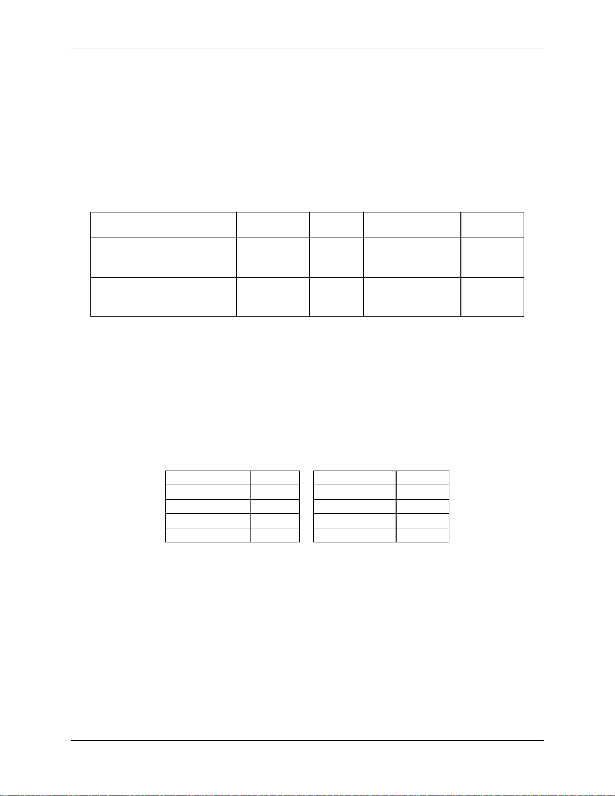
Table 3: ADC RAM Locations
0x00 IA 0x09 AUX
0x01 VB 0x0A TEMP
0x02 IB 0x0B VBAT
0x03 VA
1.2.5 Voltage References
The device includes an on-chip precision bandgap voltage reference that incorporates auto-zero techniques.
The reference is trimmed to minimize errors c aused by component mismatch and drift. The result is a
voltage output with a predictable temperature c oefficient.
The amplifier within the reference is chopper stabilized, i.e. the polarity can be switched by the MPU using
CHOP_E[1:0] (IORAM 0x2002[5:4]). The CHOP_E[1:0] field enables the MPU to operate the chopper circuit
in regular or inverted operation, or in toggling mode. When the chopper circuit is toggled in between
multiplexer cycles, DC offsets on the measured sig nals will automatically be averaged out.
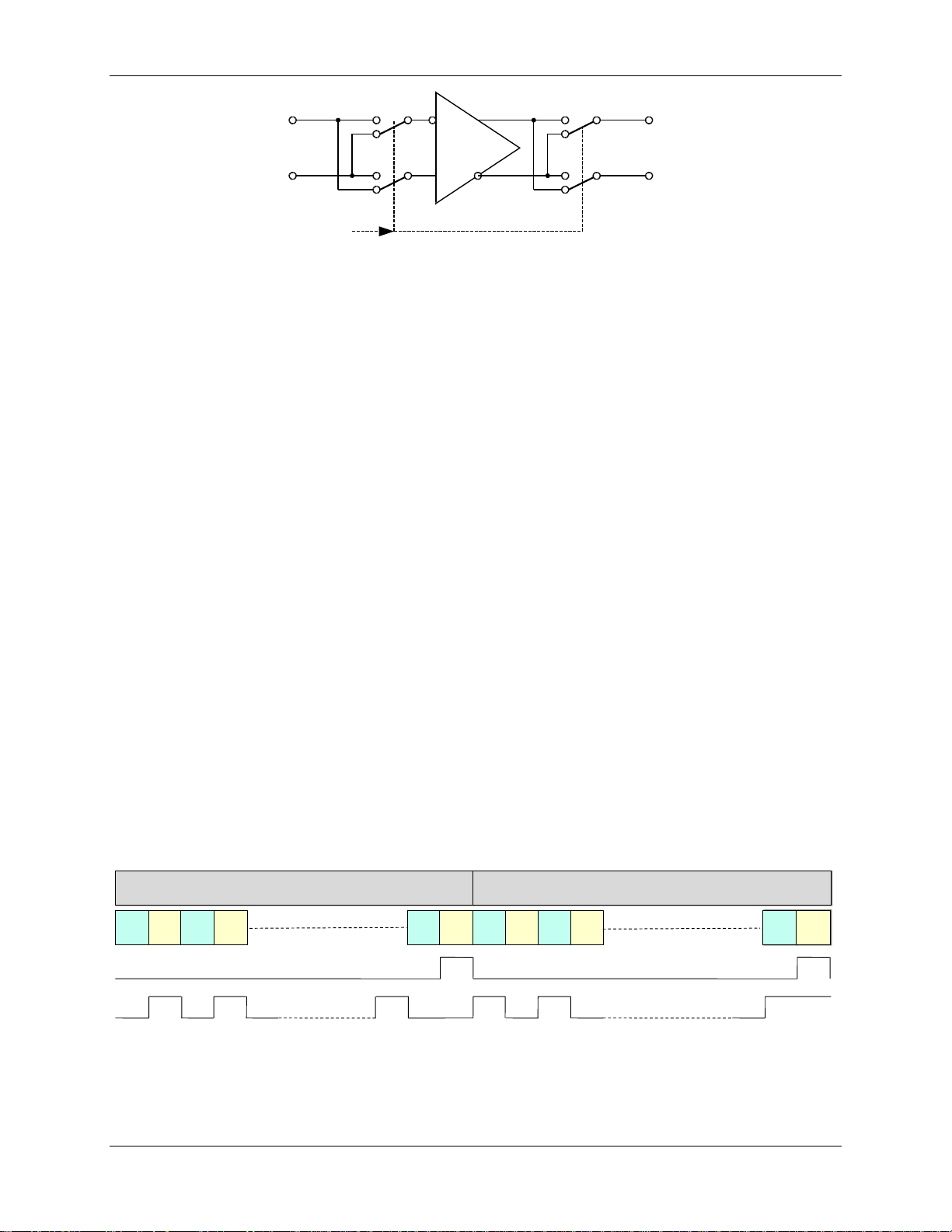
The general topology of a chopped amplifier is shown in Figure 3.
12 © 2005-2010 TERIDIAN Semiconductor Corporation v1.3
Page 13
FDS 6531/6532 005 Data Sheet 71M6531D/F-71M6532D/F
G
-
+V
inp
V
outp
V
outn
V
inn
CROSS
A
B
A
B
A
B
A
B
Mult iplexer fram es
Accumu lati on int erval n Accumul ation inter val n+1
2 43 251925201 2 43 251925201
Alt ernati ve MUX cy cle
Mult iplexer fram es
Alt ernati ve MUX cy cle
CROSS CROSS
Figure 3: General Topology of a Chopped Amplifier
It is assumed that an offset voltage Voff appears at the positive amplifier input. W ith all sw itches , as
controlled by CROSS, in the A position, the output voltage is:
Voutp – Voutn = G (Vinp + Voff – Vinn) = G (Vinp – V i nn) + G Voff
With all switches set to the B position by applying the inverted CROSS signal, the output voltage is:
Voutn – Voutp = G (Vinn – Vinp + Voff) = G (Vinn – Vinp) + G Voff, or
Voutp – Voutn = G (Vinp – Vinn) - G Voff
Thus, when CROSS is toggled, e.g. after each multiplexer cycle, the offset will alternately appear on the
output as positive and negative, which results in the offset effectively being eliminated, regardless of i ts
polarity or magnitude.
When CROSS is high, the connection of the amplifier input devices is reversed. This preserves the overall
polarity of that ampl if ier gain; it in ve r ts its i npu t o ffset . By alternately reversing the connection, the
amplifier’s offset is averaged to zero. This rem oves the most significant long-term drift mechanism in the
voltage reference. The CHOP_E[1:0] field controls the behavior of CROSS. The CROSS signal will reverse
the amplifier connection in the voltage reference in or der to negate the effects of its offset. On the first
CK32 rising edge after the last multiplexe r st ate of its sequence, the multiplexer will wait one additional
CK32 cycle before beginning a new frame. At the beginning of this cycle, the value of CROSS will be
updated according to the CHOP_E[1:0] field. The extra CK32 cycle allows time for the chopped VREF to
settle. During this cycle, MUXSYNC is held high. The leading edge of MUXSYNC initiates a pass
through the CE program sequence. The begin ni ng of the sequence is the serial readout of the four RT M
words.
CHOP_E[1:0] has four states: positive, reverse and two toggle states. In the positiv e state, CHOP_E[1:0]
= 01, CROSS and CHOP_CLK are held low. In the reverse state, CHOP_E[1:0] = 10, CROSS and
CHOP_CLK are held high. In the first toggle state, CHOP_E[1:0] = 00, CROSS is automatically toggled
near the end of each multiplexer frame and an ALT frame is forced during the last multiplexer frame in each
SUM cycle. It is desirable that CROSS take on alternate values during each ALT frame. For this reason,
if CHOP_E[1:0] = 00, CROSS will not toggle at the en d of the multiplexer frame immediately preceding
the ALT frame in each accumulation interval.
Figure 4 shows CROSS over two accumulation int erval when CHOP_E[1:0] = 00: At the end of the first
interval, CROSS is low, at the end of the second interval, CROSS is high. The offset error for the two
temperature measurements taken during the ALT multiplexer frames will be averaged to zero. Note that
v1.3 © 2005-2010 TERIDIAN Semiconductor Corporation 13
Figure 4: CROSS Signal with CHOP_E[1:0] = 00
Page 14
Data Sheet 71M6531D/F-71M6532D/F FDS 6531/6532 005
∆Σ ADC
CONVERTER
VREF
ADC_E
MUX
VREF
VBIAS
VREF
VREF_DIS
VBIAS
VREF_CAL
VBAT
VADC
MUX_DIV
MUX_ALT
EQU
22
FIR
FIR_LEN
VA
IBP
VB
IAP
IAN
IBN
TEMP
SENSOR
the number of multiplexer frames in an accumulation interval is always even. Operation with
CHOP_E[1:0] = 00 does not require control of the chopping mechanism by the MPU while eliminating the
offset for temperature measurement.
In the second toggle state, CHOP_E[1:0] = 11, no ALT frame is forced during the last multiplexer cy cle i n
an accumulation interval and CROSS always toggles near the end of each multiplexer frame.
The internal bias voltage, VBIAS (typically 1.6 V), is used by the ADC when measuring the tem perature
and battery monitor signals.
1.2.6 Temperature Sensor
The 71M6531D/F and 71M6532D/F include an on-chip temperature sensor implemented as a bandgap
reference. It is used to determine the die t em perature. The MPU may request an alternate multiplexer
cycle containing the temperature sensor output by asserting MUX_ALT.
The primary use of the temperature dat a i s to determine the magnitude of compensation req uired to offset
the thermal drift in the system (see Section 3.4 Temperature Compens ation).
1.2.7 Battery Monitor
The battery voltage is measured by the ADC during alternative multiplexer frames if the BME (Battery
Measure Enable) bit in the I/O RAM is set. While BME is set, an on-chip 45 kΩ load resistor is applied to
the battery and a scaled fraction of the batt ery voltage is applied to the ADC input. After each alternative
MUX frame, the result of the ADC conversion is avail able at XRAM address 0x0B. BME is ignored and
assumed zero when system power is not available (V1 < VBIAS). See Section 5.4.4 Battery Monitor.
1.2.8 AFE Functional Description
The AFE functions as a data acquisition system, controlled by the MPU. The main signals (IA, VA, IB and
VB) are sampled, and the ADC counts obtained are store d in X RAM where they can be accessed by the
CE and, if necessary, by the MPU. Alternate mul tiplexer cycles are initiated less frequently by the MPU to
gather access to the slow temperature and bat tery signals.
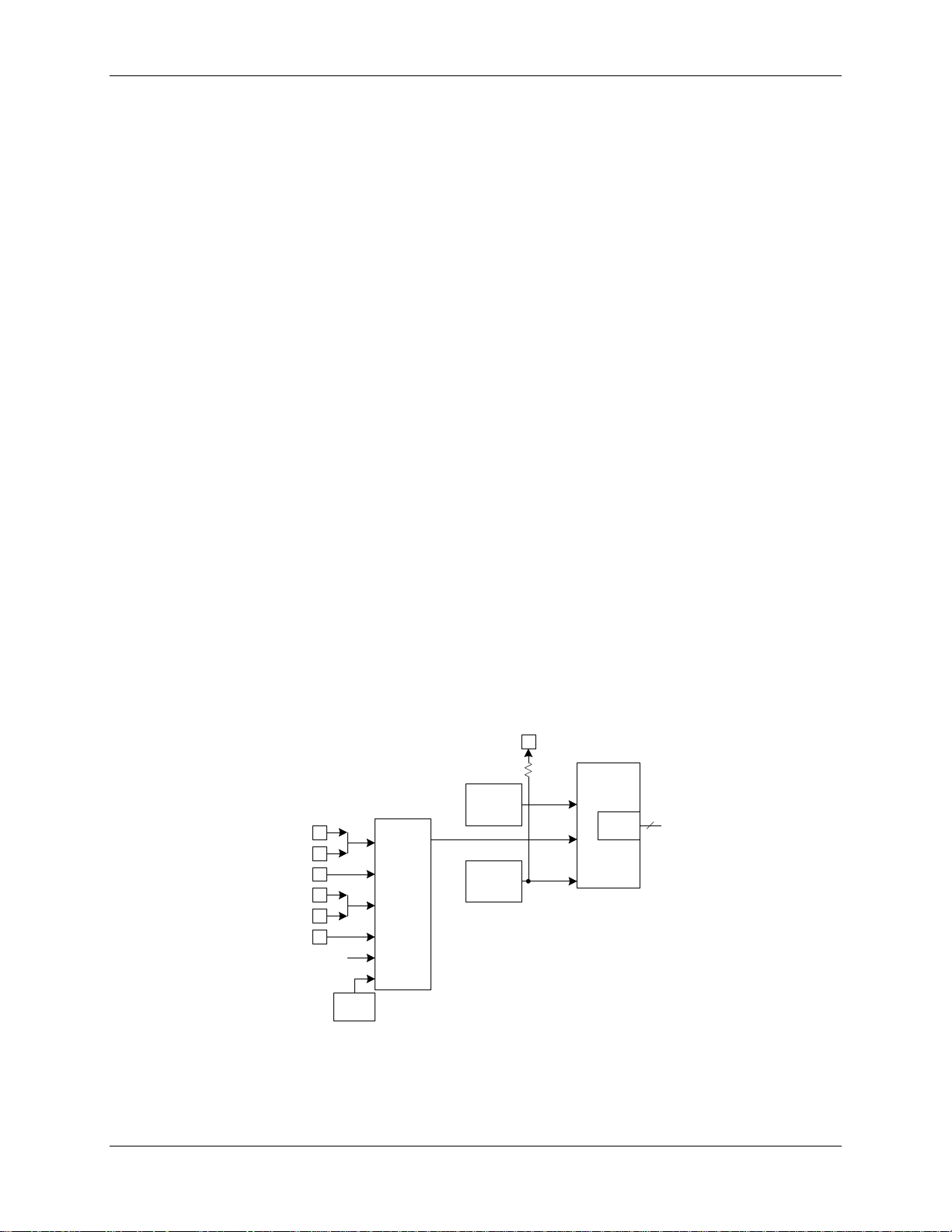
Figure 5 shows the block diagram of the AFE , with current inputs shown only as differential pair of pin s
(for the 71M6531D/F, the current input for phase A is a single pin [IA]).
Figure 5: AFE Block Diagram (Shown for the 71M6532D/F )
14 © 2005-2010 TERIDIAN Semiconductor Corporation v1.3
Page 15

FDS 6531/6532 005 Data Sheet 71M6531D/F-71M6532D/F
Address (HEX)
Name
Description
1.3 Digital Computation Engine (CE)
The CE, a dedicated 32-bit signal processor, performs the precision computations necessary to accurately
measure energy. The CE calculations and proces ses include:
• Multiplication of each current sample with its as sociated voltage sample to obtain the energy per
sample (when multiplied with the constant sampl e time).
• Frequency-insensitive delay cancellation on all four channels (to compensate for t he del ay between
samples caused by the multiplexing scheme).
• 90° phase shifter (for VAR calculations).
• Pulse generation.
• Monitoring of the input signal frequency (f or frequency and phase information).
• Monitoring of the input signal amplitude ( for sag detection).
• Scaling of the processed samples based on calibrat ion coefficients.
• Scaling of all samples based on temperature compensation information (71M6532D/F only).
The CE program resides in flash memory. Common access to flash memory by CE and MPU is controlled
by a memory share circuit. Each CE instruction word is two bytes long. Allocated flash space for the CE
program cannot exceed 4096 16-bit words (8 KB). The CE progra m count er begins a pass through the
CE code each time multiplexer state 0 begins. The code pass ends when a HALT instruction is executed.
For proper operation, the code pass must be completed before the multiplexer cycle ends (see Section
2.2 System Timing Summary).
The CE program must begin on a 1-KB boundary of the flash address. The I/O RAM register CE_LCTN[7:0]
defines which 1-KB boundary contains the CE cod e. Thus, the first CE instruction is located at
1024*CE_LCTN[7:0].
The CE can access up to 4 KB of data RAM (XRAM), or 1024 32-bit data words, starting at RAM addres s
0x0000.
The XRAM can be accessed by the FIR filter block, the RTM circuit, the CE, and the MPU. Assigned time
slots are reserved for FIR, and MPU, respectively, to prevent bus contention for XRAM data access.
The MPU can read and write the XRAM as the primary means of data communication between the two
processors. Table 4 shows the CE addresses in XRAM allocated to analog inputs from the AFE.
Table 4: XRAM Locations for ADC Results
0x00 IA Phase A current
0x01 VA Phase A voltage
0x02 IB Phase B current
0x03 VB Phase B voltage
0x04...0x09 – Not used
0x0A TEMP Temperature
0x0B VBAT Battery Voltage
The CE is aided by support hardware to facilita te implemen tation o f equa tions, pu lse co unters and
accumulators. This hardware is controlled through I/O RAM locati ons EQU[2:0] (equation assist), the
DIO_PV and DIO_PW (pulse count assist) bits and PRE_SAMPS[1:0] and SUM_CYCLES[5:0] (accumulation
assist).
PRE_SAMPS[1:0] and SUM_CYCLES[5:0] support a dual level accumula tion sc heme where the firs t
accumulator accumulates results from PRE_SAMPS[1:0] samples and the second accumulator accumulates
up to SUM_CYCLES[5:0] of the first accumulator results. The integration time for each energy output is
PRE_SAMPS[1:0] * SUM_CYCLES[5:0]/2520.6 (with MUX_DIV[3:0] = 1). The CE hardware issues the
XFER_BUSY interrupt when the accumulation is c om plete.
v1.3 © 2005-2010 TERIDIAN Semiconductor Corporation 15
Page 16
Data Sheet 71M6531D/F-71M6532D/F FDS 6531/6532 005
2
1 element, 2 W,
current sense
1 element, 3 W,
2 element, 3 W,
3φ Delta
1.3.1 Meter Equations
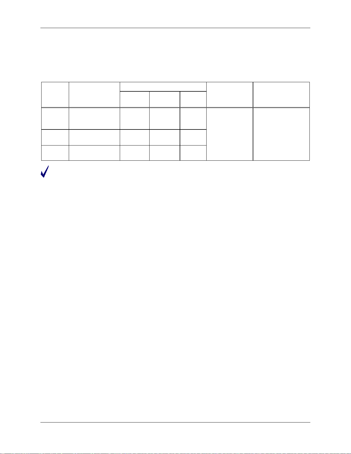
The 71M6531D/F and 71M6532D/F provide hardware assistance to the CE in order to support various
meter equations. This assistance is controll ed through I/O RAM location EQU[2:0] (equation assist). The
Compute Engine (CE) firmware for residential configurations implements the equations listed in Table 5.
EQU[2:0] specifies the equation to be used based on the number of phases used for meteri ng.
Table 5: Meter Equations
EQU[2:0] Description
0
1
2
Not all CE codes support all equations.
1φ with neutral
1φ
Element 0 Element 1 Element
VA · IA VA · IB N/A
VA(IA-
VA · IA VB · IB N/A
Watt and VAR Formula
IB)/2
N/A N/A
Mux
Sequence
Sequence is
programmable
with
SLOTn_SEL[3:0]
ALT Mux
Sequence
Sequence is
programmable with
SLOTn_ALTSEL[3:0]
1.3.2 Real-Time Monitor
The CE contains a Real-Time Monitor (RTM), which can be programmed to monitor four selectable XRAM
locations at full sample rate. The four monitored locations are serially output to the TMUXOUT pin via the
digital output multiplexer at the beginning of each CE code pass. The RTM can be enabled and disabled
with the RTM_E bit. The RTM output is clocked by CKTEST (pin SEG19/CKTEST), with the clock output
enabled by setting CKOUT_E = 1. Each RTM word is clocked out in 35 cycles and contains a leading flag
bit. See Figure 20 for the RTM output format. RTM is low when not in use.
1.3.3 Pulse Generators
The 71M6531D/F and 71M6532D/F provide four pulse generators, RPULSE, WPULSE, XPULSE and
YPULSE, as well as increased hardware support for the two original pulse generators (RPULSE and
WPULSE). The pulse generators can be used to output CE status indicators, SAG for example, to DIO pins.
The polarity of the pulses may be inverted with the PLS_INV bit. When this bit is set, the pul ses are active
high, rather than the more usual active low. PLS_INV inverts all the pulse output s.
XPULSE and YPULSE
Pulses generated by the CE may be exported to t he XPULSE and YPULSE pulse outputs. Pins DIO8
and DIO9 are used for these pulses. Generally, t he XPULSE and YPULSE outputs are updated once on
each pass of the CE code, resulting in a pulse f requency up to a maximum of 1260Hz (assuming a MUX
frame is 13 CK32 cycles).
The YPULSE pin can be used by the CE code to generate i nterrupts based on sag events. This method
is faster than checking the sag bits by the MPU at every CE_BUSY interrupt. See Section 4.3.6 CE Status
and Control for details.
RPULSE and WPULSE
During each CE code pass, the hardware stores ex ported WPULSE AND RPULSE sign bits in an 8-bit
FIFO and outputs them at a specified interval. This permits the CE code to calculate the RPULSE and
WPULSE outputs at the beginning of its code pass a nd to rely on hardware to spread them over the MUX
frame. The FIFO is reset at the beginning of each MUX frame. The PLS_INTERVAL register controls the
delay to the first pulse update and the interv al between subsequent updates. Its LSB is 4 CK_FIR cycles.
If zero, the FIFO is deactivated and the DFF s are updated immediately. Thus, N
4 * PLS_INTERVAL.
16 © 2005-2010 TERIDIAN Semiconductor Corporation v1.3
INTERVAL is
Page 17

FDS 6531/6532 005 Data Sheet 71M6531D/F-71M6532D/F
o
delay
o
delay
ft
T
t
360360 ⋅⋅=⋅=
φ
Since the FIFO resets at the beginning of each MUX frame, the user must specify PLS_INTERVAL so that
all of the pulse updates are output
before
the MUX frame completes. For instance, if the CE code outputs
5 updates per MUX interval and if the MUX int erval is 1950 cycles long, the ideal value for the interval i s
1950/5/4 = 97.5. If PLS_INTERVAL = 98, the fifth output will occur too late and be lost. In this case, the
proper value for PLS_INTERVAL is 97.
Hardware also provides a maximum pulse width feature. The PLS_MAXWIDTH register selects a maximum
negative pulse width to be Nmax updates according to the formula: Nmax = (2*PLS_MAXWIDTH+1). If
PLS_MAXWIDTH = 255, no width checking is performed.
The WPULSE and RPULSE pulse generator outputs are available on DIO6 and DIO7, respectively. They
can also be output on OPT_TX (see OPT_TXE[1:0] for details).
1.3.4 Data RAM (XRAM)
The CE and MPU use a single general-purpose Data RAM (also referred to as XRAM). The Data RAM is
1024 32-bit words, shared between the CE and the MPU using a time-multiplex method. This reduces
MPU wait states when accessing CE data. When the MPU and CE are clocking at maximum frequency
(10 MHz), the DRAM will make up to four accesses during each 100 ns interval. These consist of two
MPU accesses, one CE access and one SPI access.
The Data RAM is 32 bits wide and uses an ext ernal multiplexer so as to appear byte-wide to the MPU.
The Data RAM hardware will convert an MPU byte write operation into a read-modify-write operation that
requires two Data RAM accesses. The second ac cess is guaranteed to be available because the MPU
cannot access the XRAM on two consecutive instructions unless it is using the same address.
In addition to the reduction of wait states, t hi s arr angement permits the MPU to easily use unneeded CE
data memory. Likewise, the amount of memory the CE uses is not limited by the size of a dedicated CE
data RAM.
1.3.5 Delay Compensation
When measuring the energy of a phase (i.e., Wh and VARh) in a service, the voltage and current for that
phase must be sampled at the same instant. Otherwise, the phase difference, Ф, introduces errors.
Where f is the frequency of the input signal and t
is the sampling delay between voltage and current.
delay
In traditional meter ICs, sampling is accomplished by using two A/ D converters per phase (one for voltage
and the other one for current) controlled to sample simultaneously. Teridian’s patented Single-Converter
Technology
®
, however, exploits the 32-bit signal processi ng capability of its CE to implement “constant
delay” all-pass filters. These all-pass filters correct for the conversion time difference between the voltage
and the corresponding current samples that are obtained with a single multiplexed A/D converter.
The “constant delay” all-pass filters provide a broad-band delay β, that is precisely matched to the differ-
ence in sample time between the voltage and the current of a given phase. This digital filter does not affect the amplitude of the signal, but provi des a precisely controlled phase response. The delay compensation implemented in the CE aligns the voltage samples with their corresponding current samples by
routing the voltage samples through the all-pass filter, thus delaying the voltage samples by β, resulting in
the residual phase error β – Ф. The residual phase error is negligible, and is typically less than ±1.5 m il l idegrees at 100Hz, thus it does not contribute to errors in the energy measurements.
1.3.6 CE Functional Overview
The ADC processes one sample per channel per mul tiplexer cycle. Figure 6 shows the timing of the
samples taken during one multiplexer cycle.
The number of samples processed during one a ccumulation cycle is controlled by PRE_SAMPS[1:0]
(IORAM 0x2001[7:6]) and SUM_CYCLES[5:0] (IORAM 0x2001[5:0]). The integration time for each energy
output is:
PRE_SAMPS[1:0] * SUM_CYCLES[5:0] / 2520.6, where 2520.6 is the sample rate [Hz]
v1.3 © 2005-2010 TERIDIAN Semiconductor Corporation 17
Page 18
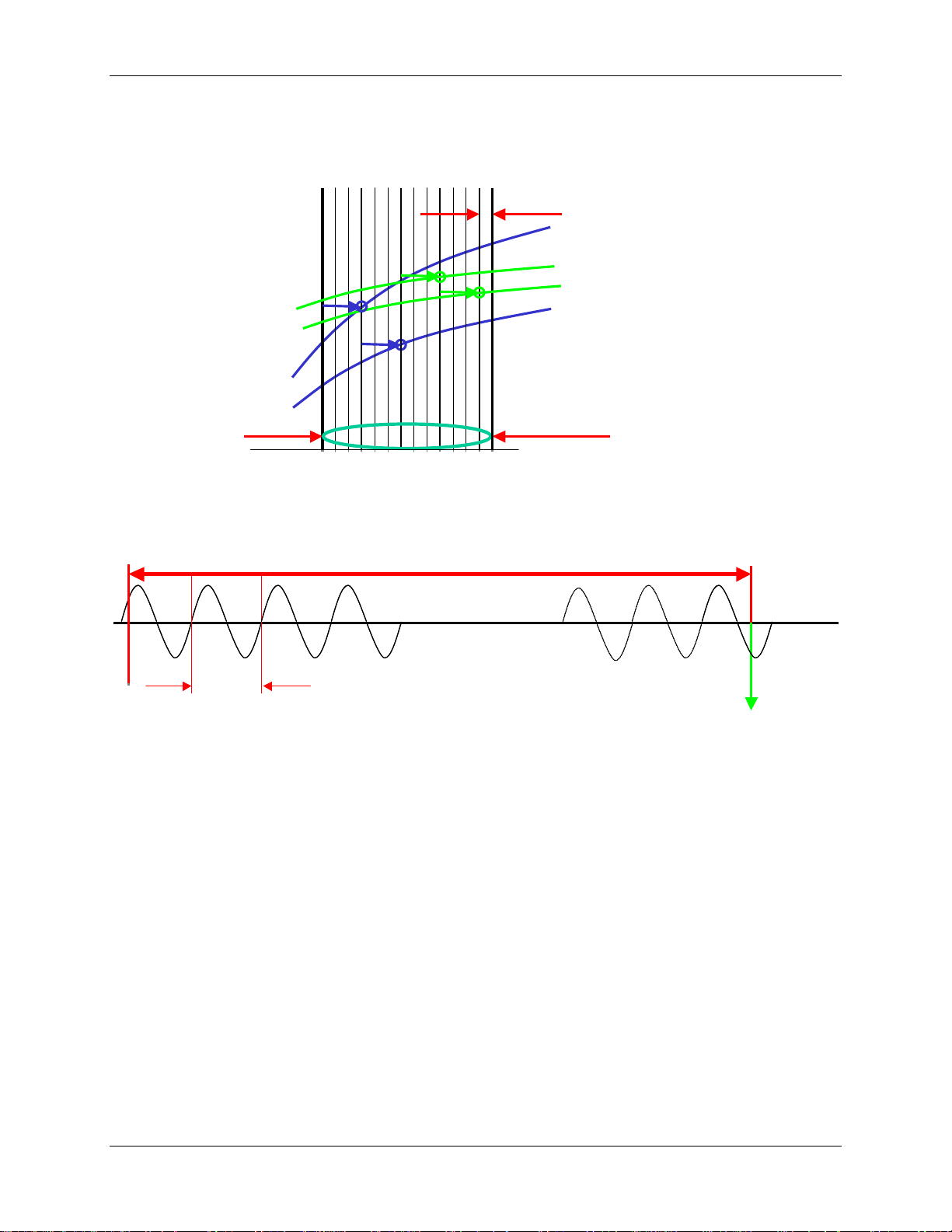
Data Sheet 71M6531D/F-71M6532D/F FDS 6531/6532 005
VA
IA
1/32768Hz =
30.518µs
13/32768Hz = 397µs
per mux cycle
IB
VB
XFER_BUSY
Interrupt to MPU
20ms
833ms
For example, PRE_SAMPS[1:0] = 42 and SUM_CYCLES[5:0] = 50 will establish 2100 sampl es per accumulati on
cycle. PRE_SAMPS[1:0] = 100 and SUM_CYCLES[5:0] = 21 will result in the exact same accumulation
cycle of 2100 samples or 833 ms. After an accumulation cycle is completed, the XFER_BUSY interrupt
signals to the MPU that accumulated data are av ai l able.
Figure 6: Samples from Multiplexer Cycle
The end of each multiplexer cycle is signaled to the MPU by the CE_BUSY interrupt. At the end of each
multiplexer cycle status information, such as sag data and the digitized input signal, is available to the MPU.
Figure 7: Accumulation Interval
Figure 7 shows the accumulation interval resulting from PRE_SAMPS[1:0] = 42 and SUM_CYCLES[5:0] =
50, consisting of 2100 samples of 397 µs each, followed by the XFER_BUSY interrupt. The sampling in
this example is applied to a 50 Hz signal.
There is no correlation between the line signal frequency and the choice of PRE_SAMPS[1:0] or
SUM_CYCLES[5:0] (even th ough when SUM_CYCLES[5:0] = 42 one set of SUM_CYCLES[5:0] happens to
sample a period of 16.6 ms). Furthermore, sampling does n ot have to start when the line voltage crosses
the zero line and the length of the accumulation interval need not be an integer multiple of the signal cycles.
18 © 2005-2010 TERIDIAN Semiconductor Corporation v1.3
Page 19

FDS 6531/6532 005 Data Sheet 71M6531D/F-71M6532D/F
M40MHZ, M26MHZ
1.4 80515 MPU Core
The 71M6531D/F and 71M6532D/F include an 80515 MPU (8-bit, 8051-compatible) that processes most
instructions in one clock cycle. Using a 10-MHz clock results in a processing throughput of 10 MIPS. The
80515 architecture eliminates redundant bus states and implements parallel execution of fetch and execution
phases. Normally, a machine c ycle i s alig ned wit h a memory fetch, therefore, most of the 1-byte instructions
are performed in a single machine cycle (MPU clock cycle). This leads to an 8x average performance
improvement (in terms of MIPS) over the Intel
Table 6 shows the CKMPU frequency as a f unct ion of the allowed combinations of the MPU clock divi der
MPU_DIV[2:0] and the MCK divider bits M40MHZ and M26MHZ. Actual processor clocking speed can be
adjusted to the total processing demand of the application (metering calculations, AMR management, memory management, LCD driver management and I/ O m anagement) using the I/O RAM field MPU_DIV[2:0]
and the MCK divider bits M40MHZ and M26MHZ, as shown in Table 6.
Table 6: CKMPU Clock Frequencies
MPU_DIV [2:0]
000 9.8304 MHz 6.5536 MHz 4.9152 MHz
001 4.9152 MHz 3.2768 MHz 2.4576 MHz
010 2.4576 MHz 1.6384 MHz 1.2288 MHz
011 1.2288 MHz 819.2 kHz 614.4 kHz
100 614.4 kHz 409.6 kHz 307.2 kHz
101 307.2 kHz 204.8 kHz 153.6 kHz
110 153.6 kHz 102.4 kHz 76.80 kHz
111 153.6 kHz 102.4 kHz 76.8 kHz
Typical measurement and metering functions based on the results provided by the internal 32-bit compute
engine (CE) are available for the MPU as part of Teridian’s standard library. Teridian provides demonstration
source code to help reduce the design cycle.
8051 device running at the same clock frequency.
[
] Values
[1,0] [0,1] [0,0]
1.4.1 Memory Organization and Addressing
The 80515 MPU core incorporates the Harvard architecture with separate code and data spaces. Memory
organization in the 80515 is similar to that of the industry standard 8051. There are four memory areas:
Program memory (Flash, shared by MPU and CE), external RAM (Data RAM, shared by the CE and MPU,
Configuration or I/O RAM), and internal data memory (Internal RAM). Table 7 shows the memory map.
Program Memory
The 80515 can address up to 64 KB of program memory space from 0x0000 to 0xFFFF. Program memory
is read when the MPU fetches instructions or p erforms a MOVC operation. Access to program memory
above 0x7FFF is controlled by the FL_BANK[2:0] register (SFR 0xB6).
After reset, the MPU starts program execution from program memory location 0x0000. The lower part of
the program memory includes reset and interrupt vectors. Th e interrupt vectors are spaced a t 8-byte
intervals, starting from 0x0003.
MPU External Data Memory (XRAM )
Both internal and external memory is physically located on the 71M6531 d evice. The external memory
referred to in this documentation is only external to the 80515 MPU core.
4 KB of RAM starting at address 0x0000 is shared by the CE and MPU. The CE normally uses the first
1 KB, leaving 3 KB for the MPU. Different versions of the CE code use varying amounts. Consult the
documentation for the specific code version being used for the exact limit.
If the MPU overwrite s th e CE’s worki ng RA M, the CE’s output may b e co rrupte d. If t he CE is disa bled,
the first 0x40 bytes of RAM are still unu sable while MUX_DIV[3:0] ≠ 0 because the 71M6531 ADC
writes to these locations. Setting MUX_DIV[3:0] = 0 disabl es th e ADC output prev entin g the CE from
writing the first 0x4 0 byte s of RA M.
v1.3 © 2005-2010 TERIDIAN Semiconductor Corporation 19
Page 20
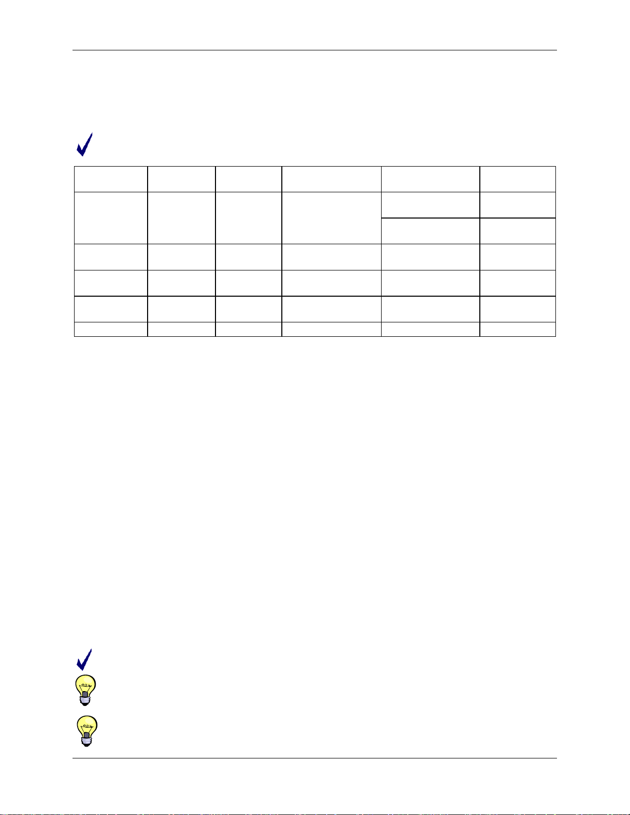
Data Sheet 71M6531D/F-71M6532D/F FDS 6531/6532 005
(hex)
Technology
Type
(bytes)
KB boundary)
The 80515 writes into external data memory when the MPU executes a MOVX @Ri,A or MOVX
@DPTR,A instruction. The MPU reads ext ernal data memory by executing a MOVX A,@Ri or MOVX
A,@DPTR instruction (SFR PDATA provides the upper 8 bytes for the MOVX A,@Ri instruction).
Internal and External Memory Map
Table 7 shows the address, type, use and size of the various memory components.
Only the memory ranges shown in Table 7 contain physical memory.
Table 7: Memory Map
Address
Memory
Memory
Name Typical Usage
Memory Size
00000-1FFFF/
00000-3FFFF
Flash
Memory
Non-volatile
0000-0FFF Static RAM Volatile
2000-20BF,
20C8-20FF
20C0-20C7 Static RAM
Static RAM Volatile
Non-volatile
(battery)
Program memory
for MPU and CE
External RAM
(XRAM)
Configuration RAM,
I/O RAM
Configuration RAM,
I/O RAM
MPU Program and
non-volatile data
CE program (on 1
Shared by CE and
MPU
Hardware control 256
Battery-buffered
memory
128 KB/
256 KB
†
8 KB max.
4 KB
8
0000-00FF Static RAM Volatile Internal RAM Part of 80515 Core 256
†
Memory size depends on the IC. See Section1.5.5 Physical Memory for details.
MOVX Addressing
There are two types of instructions differing in whether they provide an 8-bit or 16-bit indirect address to
the external data RAM.
In the first type, MOVX A,@Ri, the contents of R0 or R1 in the current register bank provi de the eight
lower-ordered bits of address. The eight high-ordered bits of the address are specified with the PDATA
SFR. This method allows the user paged access (256 page s of 256 bytes each) to all ranges of the
external data RAM.
In the second type of MOVX instruction, MOVX A,@DPTR, the data pointer generates a 16-bit address.
This form is faster and more efficient when accessing very large data arrays (up to 64 KB), since no
additional instructions are needed to set up the eight high ordered bits of the address.
It is possible to mix the two MOVX types. This provides the user with four sep arate data pointers, two
with direct access and two with paged access, to the entire 64 KB of external memory range.
Dual Data Pointer
The Dual Data Pointer accelerates the block mov es of data. The standard DPTR is a 16-bit register that
is used to address external memory or peripheral s. In the 80515 core, the standard data pointer is called
DPTR, the second data pointer is called DPTR1. The data pointer select bit, located in the LSB of the DPS
register (DPS[0]), chooses the active pointer. DPTR is select ed when DPS[0] = 0 and DPTR1 is selected
when DPS[0] = 1.
The user switches between pointers by toggling the LSB of the DPS register. The values in the data pointers
are not affected by the LSB of the DPS register. All DPTR relat ed instructions use the currently selected
DPTR for any activity.
The second data pointer may not be supported by certain compilers.
DPTR1 is useful for copy routines, where it can make t he inner loop of the routine t wo instructions faster
compared to the reloading of DPTR from registers. Any interrupt routine using DPTR1 must save
and restore DPS, DPTR and DPTR1, which increases stack usage and slows down interrupt latency.
By selecting the Evatronics R80515 core in the Kei l compi l er project settings and by using the
compiler directive “MODC2”, dual d ata point ers are enabled in certain library routines.
20 © 2005-2010 TERIDIAN Semiconductor Corporation v1.3
Page 21
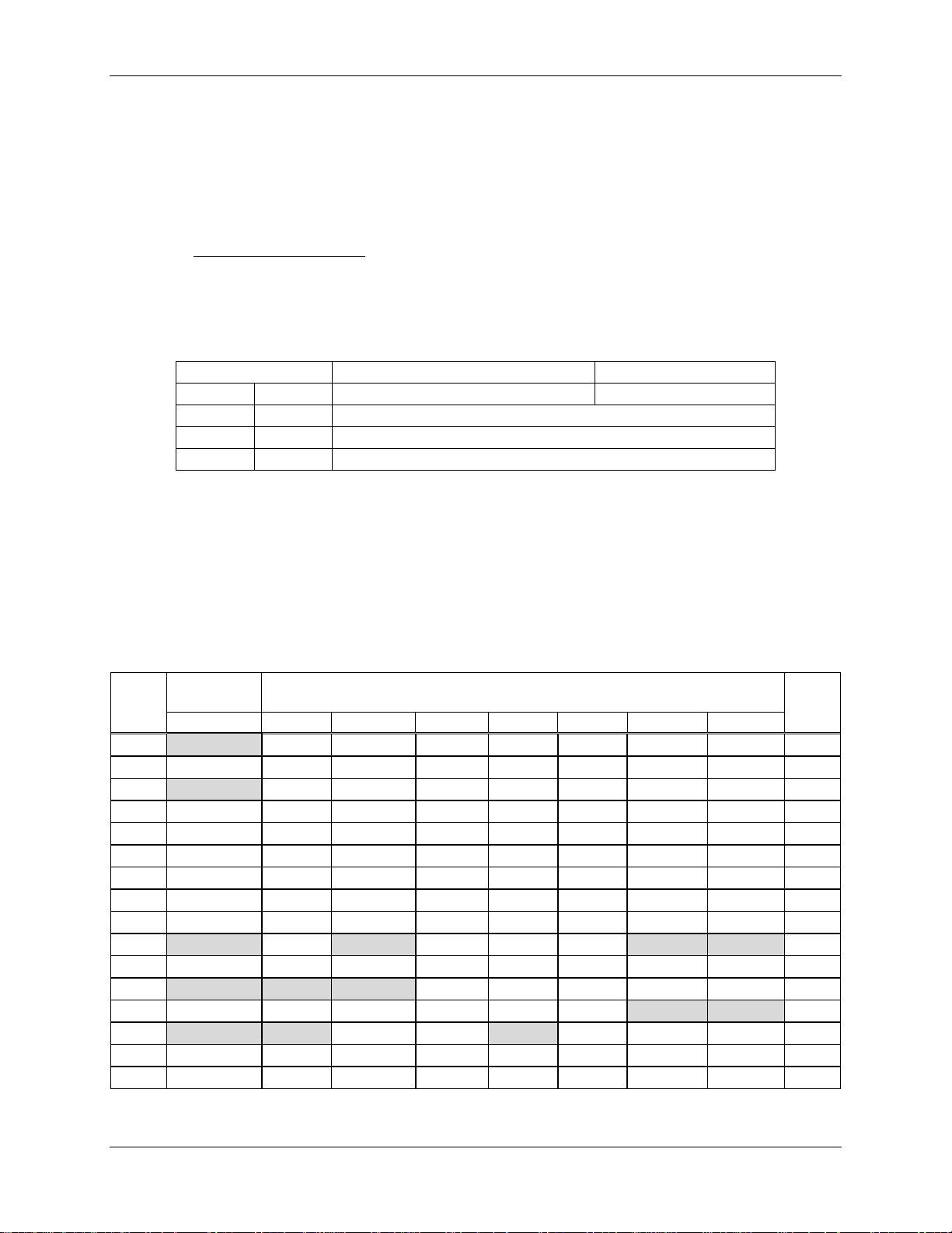
FDS 6531/6532 005 Data Sheet 71M6531D/F-71M6532D/F
Addressable
X000
X001
X010
X011
X100
X101
X110
X111
F8
INTBITS
FF
F0
F7
D8
WDCON
DF
D0
D7
B8
IEN1
IP1
S0RELH
S1RELH
PDATA
BF
B0
B7
98
S0CON
S0BUF
IEN2
S1CON
S1BUF
S1RELL
EEDATA
EECTRL
9F
90
97
An alternative data pointer is available in the form of the PDATA register (SFR 0xBF), sometimes referred
to as USR2). It defines t he hi gh byt e of a 16-bit address when reading or writing XDATA with the instruction
MOVX A,@Ri or MOVX @Ri,A.
Internal Data Memory Map and Access
The Internal data memory provides 256 bytes (0x00 to 0xFF) of data memory. The internal data memory
address is always 1 byte wide. Table 8 shows the internal data memory map.
The Special Function Registers (SFR) occupy the upper 128 bytes. The SFR area of internal data memory
is available
only by direct addressing
. Indirect addressing of this area accesses the upper 1 28 bytes of
Internal RAM. The lower 128 bytes contain working registers and bit addressable memory. The lower 32
bytes form four banks of eight registers (R0-R7). Two bits on the program memory status word (PSW) select
which bank is in use. The next 16 bytes form a block of bit addressable memory space at bit addresses
0x00-0x7F. All of the bytes in the lower 128 bytes are accessible through direct or indirect addressing.
Table 8: Internal Data Memory Map
Address Range Direct addressing Indirect addressing
0x80 0xFF Special Function Registers (SFRs) RAM
0x30 0x7F Byte addressable area
0x20 0x2F Bit addressable area
0x00 0x1F Register banks R0…R7
1.4.2 Special Function Registers (SFRs)
A map of the Special Function Registers is show n i n Table 9.
Only a few addresses in the SFR memory space are occupied, the others are not implemented. A read
access to unimplemented addresses will return undefined data, while a write access will have no effect.
SFRs specific to the 71M6531D/F and 71M6532D/F are shown in bold print on a gray field. The registers
at 0x80, 0x88, 0x90, etc., are bit addressable, all others are by te addressable. See the restrictions for the
INTBITS register in Table 14.
Table 9: Special Function Register Map
Hex/
Bin
Bit
Byte Addressable
Bin/
Hex
B
E8 IFLAGS
E0
A
EF
E7
PSW
C8
C0
A8
A0 P2 DIR2 DIR0
T2CON
IRCON
P3
FLSHCTL
FL_BANK PGADR
IEN0 IP0 S0RELL
CF
C7
AF
A7
88
80
P1 DIR1
DPS
ERASE
TCON TMOD TL0 TL1 TH0 TH1 CKCON
P0 SP DPL DPH DPL1 DPH1 PCON
8F
87
v1.3 © 2005-2010 TERIDIAN Semiconductor Corporation 21
Page 22

Data Sheet 71M6531D/F-71M6532D/F FDS 6531/6532 005
1.4.3 Generic 80515 Special Function Registers
Table 10 shows the location, description and reset or power-up value of the generic 80515 SFRs. Additional
descriptions of the registers can be found at the page num bers listed in the table.
Table 10: Generic 80515 SFRs - Location and Reset Values
Name
P0
SP
DPL
DPH
DPL1
DPH1
PCON
TCON
TMOD
TL0
TL1
TH0
TH1
CKCON
P1
DPS
S0CON
S0BUF
IEN2
S1CON
S1BUF
S1RELL
P2
IEN0
IP0
S0RELL
P3
IEN1
IP1
S0RELH
S1RELH
PDATA
IRCON
T2CON
PSW
WDCON
A
B
Address
(Hex)
0x80 0xFF Port 0 24
0x81 0x07 Stack Pointer 23
0x82 0x00 Data Pointer Low 0 23
0x83 0x00 Data Pointer High 0 23
0x84 0x00 Data Pointer Low 1 23
0x85 0x00 Data Pointer High 1 23
0x87 0x00 UART Speed Control, Idle and Stop mode Control 28
0x88 0x00 Timer/Counter Control 31
0x89 0x00 Timer Mode Control 29
0x8A 0x00 Timer 0, low byte 28
0x8B 0x00 Timer 1, high byte 28
0x8C 0x00 Timer 0, low byte 28
0x8D 0x00 Timer 1, high byte 28
0x8E 0x01 Clock Control (Stretch=1) 24
0x90 0xFF Port 1 23
0x92 0x00 Data Pointer select Register 20
0x98 0x00 Serial Port 0, Control Register 27
0x99 0x00 Serial Port 0, Data Buffer 26
0x9A 0x00 Interrupt Enable Register 2 31
0x9B 0x00 Serial Port 1, Control Register 27
0x9C 0x00 Serial Port 1, Data Buffer 26
0x9D 0x00 Serial Port 1, Reload Register, low byte 26
0xA0 0xFF Port 2 23
0xA8 0x00 Interrupt Enable Register 0 30
0xA9 0x00 Interrupt Priority Register 0 33
0xAA 0xD9 Serial Port 0, Reload Register, low byte 26
0xB0 0xFF Port 3 23
0xB8 0x00 Interrupt Enable Register 1 31
0xB9 0x00 Interrupt Priority Register 1 33
0xBA 0x03 Serial Port 0, Reload Register, high byte 26
0xBB 0x03 Serial Port 1, Reload Register, high byte 26
0xBF 0x00 High address byte for MOVX@Ri - also called USR2 20
0xC0 0x00 Interrupt Request Control Register 31
0xC8 0x00 Polarity for INT2 and INT3 31
0xD0 0x00 Program Status Word 23
0xD8 0x00 Baud Rate Control Register (only WDCON[7] bit used) 26
0xE0 0x00 Accumulator 23
0xF0 0x00 B Register 23
Reset value
(Hex)
Description Page
22 © 2005-2010 TERIDIAN Semiconductor Corporation v1.3
Page 23
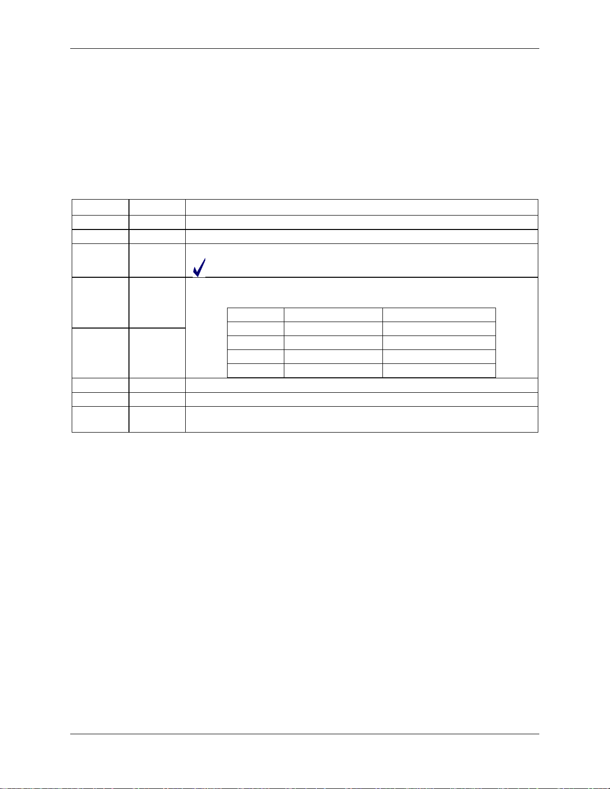
FDS 6531/6532 005 Data Sheet 71M6531D/F-71M6532D/F
Accumulator (ACC, A, SFR 0xE0):
ACC is the accumulator register. Most instructions use the accum ulator to hol d the operand . The
mnemonics for accumulator-specific instructions refer to accumulator as A, not ACC.
B Register (SFR 0xF0):
The B register is used during multiply and divide instructions. It can also be used as a scratch-pad register
to hold temporary data.
Program Status Word (PSW, SFR 0xD0):
This register contains various flags and control bits for the selection of the register banks (see Table 11).
Table 11: PSW Bit Functions (SFR 0xD0)
PSW Bit
7
6
Symbol Function
CV
AC
Carry flag.
Auxiliary Carry flag for BCD operations.
General-purpose Flag 0 available for user.
5
F0
F0 is not to be confused with the F0 flag in the CESTATUS register.
Register bank select control bits. The contents of RS1 and RS0 select the
4
RS1
working register bank:
RS1/RS0 Bank selected Location
00 Bank 0 0x00 – 0x07
01 Bank 1 0x08 – 0x0F
3
2
RS0
OV
Overflow flag.
10 Bank 2 0x10 – 0x17
11 Bank 3 0x18 – 0x1F
1 - User defined flag.
0
P
Parity flag, affected by hardware to indicate odd or even number of one bits in
the Accumulator, i.e. even parity.
Stack Pointer (SP, SFR 0x81):
The stack pointer is a 1-byte register initialize d to 0x07 after reset. This register is incremented before
PUSH and CALL instructions, causing the stack to begin at location 0x08.
Data Pointer:
The data pointers (DPTR and DPRT1) are 2 bytes wide. The lower part is DPL(SFR 0x82) and DPL1
(SFR0x84) and the highest is DPH (SFR0x83) and DPH1 (SFR 0x85). The data pointers can be loaded as
two registers (e.g. MOV DPL,#data8). They are g enerally used to access external code or data space
(e.g. MOVC A,@A+DPTR or MOVX A,@DPTR respectively).
Program Counter:
The program counter (PC) is 2 bytes wide and i nitialized to 0x0000 after reset. The PC is incremented
when fetching operation code or when operating on data from program memory.
Port Registers:
The I/O ports are controlled by Special Function Registers P0, P1 and P2 as shown in Table 12. The contents
of the SFR can be observed on corresponding pins o n the chip. Writing a 1 to any of the ports causes the
corresponding pin to be at high level (V3P3). Writing a 0 causes the corresponding pin to be held at a low
level (GND). The data direction registers DIR0, DIR1 and DIR2 define individual pins as input or output
pins (see Sections 1.5.7 Digital I/O – 71M6531D/F or 1.5.8 Digital I/O – 71M6532D/F).
v1.3 © 2005-2010 TERIDIAN Semiconductor Corporation 23
Page 24
Data Sheet 71M6531D/F-71M6532D/F FDS 6531/6532 005
Address
P0
DIR0
000
0 1 1 2 1
001
1 2 2 3 1
010
2 3 3 4 2
100
4 5 5 6 4
110
6 7 7 8 6
(Alternate Name)
Address
Table 12: Port Registers
Register
P1
DIR1
P2
DIR2
All DIO ports on the chip are bi-directional. Each of them consists of a Latch (SFR P0 to P2), an output
driver and an input buffer, therefore the MP U ca n output or read data through any of these ports. Even if
a DIO pin is configured as an output, the state of the pin can still be read by the MPU, for example wh en
counting pulses issued via DIO pins that are under CE control.
The technique of reading the status of or generatin g i nterrupts based on DIO pins configured as
outputs can be used to implement pulse counting.
Clock Stretching (CKCON[2:0], SFR 0x8E)
The CKCON[2:0] field defines the stretch memory cycles that could be used for MOVX instructions when
accessing slow external peripherals. The practical value of this register for the 71M653x is to guarantee
access to XRAM between CE, MPU, and SPI. The default setting of CKCON[2:0] (001) should not be
changed.Table 13 shows how the signals of t he External Memory Interface change when stretch v al ues
are set from 0 to 7. The widths of the signals are counted in MPU clock cycles. The post-reset state of
the CKCON[2:0] field (001), which is shown in bold in the table, performs the MOVX instructions with a
stretch value equal to 1.
SFR
0x80 R/W Register for port 0 read and write operations.
0xA2 R/W
0x90 R/W Register for port 1 read and write operations.
0x91 R/W Data direction register for port 1.
0xA0 R/W Register for port 2 read and write operations.
0xA1 R/W Data direction register for port 2.
CKCON[2:0]
R/W Description
Data direction register for port 0. Setting a bit to 1 indicates that the
corresponding pin is an output.
Table 13: Stretch Memory Cycle Width
Stretch
Value
Read signal width Write signal width
memaddr memrd memaddr memwr
011 3 4 4 5 3
101 5 6 6 7 5
111 7 8 8 9 7
1.4.4 Special Function Registers (SFRs) Specific to the 71M6531D/F and 71M6532D/F
Table 14 shows the location and description of the SFRs specific to the 71M6531D/F and 71M6532D/F.
Table 14: 71M6531D/F and 71M6532D/F Specific SFRs
Register
EEDATA
EECTRL
24 © 2005-2010 TERIDIAN Semiconductor Corporation v1.3
SFR
0x9E R/W
0x9F R/W
Bit Field
Name
R/W Description
I2C EEPROM interface data register.
I2C EEPROM interfac e con tr o l register. See
Section
description of the command and status bits
available for EECTRL.
1.5.14 EEPROM In terfa ce for a
Page 25

FDS 6531/6532 005 Data Sheet 71M6531D/F-71M6532D/F
0xB6[2:0]
R/W
Flash Bank Selection.
Program Write Enable:
nitors the XFER_BUSY interrupt.
the interrupt handler.
This flag indicates that the MPU was awakened
Interrupt inputs. The MPU may read these bits
and are primarily intended for debug use.
Register
(Alternate Name)
ERASE
(FLSH_ERASE)
FL_BANK
PGADDR
(FLSH_PGADR[5:0])
FLSHCRL
SFR
Address
Bit Field
Name
0x94 W
0xB7 R/W
0xB2[0]
0xB2[1]
0xB2[6]
0xB2[7]
0xE8[0]
0xE8[1]
FLSH_PWE
FLSH_MEEN
SECURE
PREBOOT
IE_XFER
IE_RTC
R/W Description
This register is used to initiate either the Flash
Mass Erase cycle or the Flash Page Erase cycle.
See the Flash Memory section for details.
Flash Page Erase Address register. Contains
the flash memory page address (page 0 through
page 127) that will be erased during the Page
Erase cycle (default = 0x00).
Must be re-written for each new Page Erase
cycle.
0: MOVX commands refer to XRAM
R/W
Space, normal operation (default).
1: MOVX @DPTR,A moves A to Program
Space (Flash) @ DPTR.
Mass Erase Enable:
0: Mass Erase disabled (default).
W
1: Mass Erase enabled.
Must be re-written for each new Mass Erase
cycle.
Enables security provisions that prevent external
R/W
reading of flash memory and CE program RAM.
This bit is reset on chip reset and may only be
set. Attempts to write zero are ignored.
R Indicates that the preboot sequence is active.
This flag mo
R/W
It is set by hardware and must be cleared by
the interrupt handler.
This flag monitors the RTC_1SEC interrupt. It
R/W
is set by the hardware and must be cleared by
0xE8[2]
IFLAGS
0xE8[3]
0xE8[4]
0xE8[5]
0xE8[6]
0xE8[7]
0xF8[6:0]
INTBITS
(INT0 … INT6)
0xF8[7]
v1.3 © 2005-2010 TERIDIAN Semiconductor Corporation 25
FWCOL1
R/W
This flag indicates that a flash write was in
progress while the CE was busy.
This flag indicates that a flash write was
FWCOL0
R/W
attempted when the CE was attempting to
begin a code pass.
IE_PB
IE_WAKE
PLL_RISE
PLL_FALL
INT6 … INT0
WD_RST
R/W
R/W
R/W
R/W
This flag indicates that the wake-up pushbutton
was pressed.
by the autowake timer.
PLL_RISE Interrupt Flag:
Write 0 to clear the PLL_RISE interrupt flag.
PLL_FALL Interrupt Flag:
Write 0 to clear the PLL_FALL interrupt flag.
to see the status of external interrupts INT0 up
R
to INT6. These bits do not have any memory
W The WDT is reset when a 1 is written to this
bit.
Only byte operations on the entire INTBITS register should be used when
writing. The byte must have all bits set except the bits that are to be
cleared.
Page 26
Data Sheet 71M6531D/F-71M6532D/F FDS 6531/6532 005
(
= 0)
(
= 1)
2
smod
* f
/ (384 * (256-TH1))
2
smod
* f
/(64 * (210-S0REL))
N/A
f
/(32 * (210-S1REL))
UART 0
UART 1
Start bit, 8 data bits, parity, stop bit, v ariable
baud rate (internal baud rate generator)
or timer 1)
fixed baud rate 1/32 or 1/64 of f
CKMPU
nerator or timer 1)
1.4.5 Instruction Set
All instructions of the generic 8051 microcontroller are supported. A complete list of the instru ction set
and of the associated op-codes is contained in the 71M653X Software User’s Guide (SUG).
1.4.6 UARTs
The 71M6531D/F and 71M6532D/F include a UART (UART0) that can be programmed to comm unicate
with a variety of AMR modules. A second UART (UA RT1) is connected to the optical port, as described
in Section 1.5.6 Optical Interface.
The UARTs are dedicated 2-wire serial interfaces, which can communicate with an external host processor
at up to 38,400 bits/s (with MPU clock = 1. 2288 MHz). The operation of the RX and T X UART0 pins is as
follows:
• UART0 RX: Serial input data are applied at this pin. Conforming to RS-232 standard, the bytes are
input LSB first.
• UART0 TX: This pin is used to output the serial data. The bytes are output LSB first.
The 71M6531D/F and 71M6532D/F have several UART-related registers for the control and buffering of
serial data.
A single SFR register serves as both the transmit buf fer and receive buffer (S0BUF, SFR 0x99 for UART0
and S1BUF, SFR 0x9C for UART1). When written by the MPU, S0BUF and S1BUF act as transmit buffers for
their respective channels, and when read by the MPU, they act as receive buffers. Writing data to the
transmit buffer starts the transmission by the associated UART. Received data are available by reading
from the receive buffer. Both UARTs can simultaneously transmit and receive data.
WDCON[7] (SFR 0xD8) selects whether timer 1 or the internal baud rate generator is used. All UART
transfers are programmable for parity enable, parity, 2 stop bits/1 stop b it and XON/X OFF opt ions f or va riabl e
communication baud rates from 300 to 38400 bps. Table 15 shows how the baud rates are calculated.
Table 16 shows the selectable UART operation modes.
Table 15: Baud Rate Generation
UART0
UART1
Using Timer 1
WDCON[7]
CKMPU
Using Internal Baud Rate Generator
WDCON[7]
CKMPU
CKMPU
S0REL and S1REL are 10-bit values derived by combining bits from the respective timer reload register s
(S0RELL, S0RELH, S1RELL, S1RELH). SMOD is the SMOD bit in the SFR PCON register. TH1 is the high
byte of timer 1.
Table 16: UART Modes
Mode 0 N/A
Mode 1
Mode 2
Start bit, 8 data bits, stop bit, variable
baud rate (internal baud rate generator
Start bit, 8 data bits, parity, stop bit,
Start bit, 8 data bits, stop bit, variable baud
rate (internal baud rate generator)
N/A
Start bit, 8 data bits, parity, stop bit, va-
Mode 3
riable baud rate (internal baud rate ge-
N/A
Parity of serial data is available through the P flag of the accumulator. 7-bit serial modes with
parity, such as those used by the FLAG proto col, can be simulated by setting and reading bit 7 of
8-bit output data. 7-bit serial modes without parity can be simulated by setting bit 7 to a constant 1.
8-bit serial modes with parity can be simulated by setting and reading the 9
th
bit, using the control
bits TB80 (S0CON[3]) and TB81 (S1CON[3]) in the S0CON (SFR 0x98) and S1CON (SFR 0x9B) SFRs
for transmit and RB81 (S1CON[2]) for receive operations.
26 © 2005-2010 TERIDIAN Semiconductor Corporation v1.3
Page 27
FDS 6531/6532 005 Data Sheet 71M6531D/F-71M6532D/F
Bit
Symbol
Function
communication etc.)
Bit
Symbol
Function
Sets the baud rate and mode for UART1.
0
A
9-bit UART
variable
1
B
8-bit UART
variable
The feature of receiving 9 bits (Mode 3 for UART0, Mode A for UART1) can be used as handshake signals
for inter-processor communication in multi-processor systems. In this case, the slave proce ssors have bit
SM20 (S0CON[5]) for UART0, or SM21 (S1CON[5] for UART1, set to 1. When the master processor outputs
the slave’s address, it sets the 9
th
bit to 1, causing a serial port receive interrupt in all the slaves. The slave
processors compare the received byte with thei r address. If there is a match, the addressed slave will
clear SM20 or SM21 and receive the rest of the message. All other slaves will ignore the message. Aft er
addressing the slave, the host outputs the rest of the message with the 9
th
bit set to 0, so no additional
serial port receive interrupts will be generated.
UART Control Registers:
The functions of UART0 and UART1 depend on the setting of the Serial Port Control Registers S0CON
and S1CON shown in Table 17 and Table 18, respectively and the PCON register shown in Table 19.
Since the TI0, RI0, TI1 and RI1 bits are in an SFR bit addressable byte, common practice
would be to clear them with a bit operation, but this
must be avoided
. The hardware implements
bit operations as a byte wide read-modify-write hardwa re m acro. If an interrupt occurs after
the read, but before the write, its flag will be clea red unintentionally.
The proper way to clear these flag bits is to write a byte mask consisting of all ones except for
a zero in the location of the bit to be cleared. The flag bits are configured in hardware to ignore
ones written to them.
Table 17: The S0CON (UART0) Register (SFR 0x98)
S0CON[7] SM0
S0CON[6] SM1
S0CON[5] SM20
S0CON[4] REN0
S0CON[3] TB80
S0CON[2] RB80
S0CON[1] TI0
S0CON[0] RI0
The SM0 and SM1 bits set the UART0 mode:
Mode Description SM0 SM1
0 N/A 0 0
1 8-bit UART 0 1
2 9-bit UART 1 0
3 9-bit UART 1 1
Enables the inter-processor communication feature.
If set, enables serial reception. Cleared by sof tware to disable reception.
The 9th transmitted data bit in Modes 2 and 3. Set or cleared by the
MPU, depending on the function it performs (parity check, multiprocessor
In Modes 2 and 3 it is the 9th data bit received. In Mode 1, SM20 is 0,
RB80 is the stop bit. In mode 0, this bit is not used. M ust be cleared by
software.
Transmit interrupt flag; set by hardware after completion of a serial transfer.
Must be cleared by software.
Receive interrupt flag; set by hardware after completion of a serial reception.
Must be cleared by software.
Table 18: The S1CON (UART1) register (SFR 0x9B)
S1CON[7] SM
S1CON[5] SM21
S1CON[4] REN1
S1CON[3] TB81
v1.3 © 2005-2010 TERIDIAN Semiconductor Corporation 27
SM Mode Description Baud Rate
Enables the inter-processor communication feature.
If set, enables serial reception. Cleared by sof tware to disable reception.
The 9th transmitted data bit in Mode A. Set or cleared by the MPU,
depending on the function it performs (parity check, multiprocessor
communication etc.)
Page 28
Data Sheet 71M6531D/F-71M6532D/F FDS 6531/6532 005
Bit
Symbol
Function
Bit
Symbol
Function
M1
M0
Mode
Function
13-bit Counter/Timer mode with 5 lower bits in the TL0 or TL1 register
1, respectively). The 3 high order bits of TL0 and TL1 are held at zero.
S1CON[2] RB81
S1CON[1] TI1
S1CON[0] RI1
PCON[7] SMOD
PCON[6:2]
PCON[1] STOP
PCON[0] IDLE
–
In Modes A and B, it is the 9th data bit received. In Mode B, if SM21 is 0,
RB81 is the stop bit. Must be cleared by software
Transmit interrupt flag, set by hardware after completion of a serial transfer.
Must be cleared by software.
Receive interrupt flag, set by hardware after completion of a serial reception.
Must be cleared by software.
Table 19: PCON Register Bit Description (SF R 0x87)
The SMOD bit doubles the baud rate when set
Not used.
Stops MPU flash access and MPU peripherals in cluding timers and
UARTs when set until an external interrupt i s received.
Stops MPU flash access when set until an internal interrupt is received.
1.4.7 Timers and Counters
The 80515 has two 16-bit timer/counter registers: Timer 0 and Timer 1. These registers can be configured
for counter or timer operations.
In timer mode, the register is incremented every 12 MPU clock cycles. In counter mode, the register is
incremented when the falling edge is observed at the corresponding input signal T0 or T1 (T0 and T1 a re
the timer gating inputs derived from certain DIO pins, see Section 1.5.7 Digital I/O). Since it takes 2 machine
cycles to recognize a 1-to-0 event, the maximum input count rate is 1/2 of the clock frequency (CKMPU).
There are no restrictions on the duty cycle, however to ensure proper recognition of the 0 or 1 state, an
input should be stable for at least 1 machine cycle.
Four operating modes can be selected for Time r 0 and Timer 1, as shown in Table 20 and Table 21. The
TMOD Register, shown in Table 22, is used to select the approp ri ate mode. The timer/counter operation
is controlled by the TCON Register, which is shown in Table 23. Bits TR1 (TCON[6]) and TR0 (TCON[4]) in
the TCON register start their associated timers when set.
Table 20: Timers/Counters Mode Description
0 0 Mode 0
0 1 Mode 1
1 0 Mode 2
1 1 Mode 3
In Mode 3, TL0 is affected by TR0 and gate control bits and sets the TF0 flag on overflow, while TH0
is affected by the TR1 bit and the TF1 flag is set on overflow.
Table 21 specifies the combinations of operation modes allowed for Timer 0 and Timer 1.
and the remaining 8 bits in the TH0 or TH1 register (for Timer 0 and Timer
16-bit Counter/Timer mode.
8-bit auto-reload Counter/Timer. The reload value is kept in TH0 or
TH1, while TL0 or TL1 is incremented every machine cycle. When TL(x)
overflows, a value from TH(x) is copied to TL(x) (where x = 0 for
counter/timer 0 or 1 for counter/timer 1.
If Timer 1 M1 and M0 bits are set to 1, Timer 1 stops.
If Timer 0 M1 and M0 bits are set to 1, Timer 0 acts as two independent
8-bit Timer/Counters.
28 © 2005-2010 TERIDIAN Semiconductor Corporation v1.3
Page 29
FDS 6531/6532 005 Data Sheet 71M6531D/F-71M6532D/F
Bit
Symbol
Function
Timer/Counter 1:
Timer/Counter 0:
Table 21: Allowed Timer/Counter Mode Combinations
Timer 1
Timer 0 - mode 0
Timer 0 - mode 1
Timer 0 - mode 2
Mode 0 Mode 1 Mode 2
Yes Yes Yes
Yes Yes Yes
Not allowed Not allowed Yes
Table 22: TMOD Register Bit Descriptio n (SFR 0x89)
If TMOD[7] is set, external input signal control is enabled for Counter 0.
external gate control. The TR1 bit in the TCON register (SFR 0x88) must
TMOD[7] Gate
also be set in order for Counter 1 to increment.
With these settings Counter 1 is incremented on every falling edge of the
logic signal applied to one or more of the interrupt sources controlled by
the DI_RBP, DIO_R1, … DIO_RXX registers.
Selects timer or counter operation. When set to 1, a counter operation is
TMOD[6] C/T
performed. When cleared to 0, the corresponding register will function as a
timer.
TMOD[5:4] M1:M0
Selects the mode for Timer/Counter 1 as shown in Table 20.
If TMOD[3] is set, external input signal control is enabled for Counter 0.
external gate control. The TR0 bit in the TCON register (SFR 0x88) must
TMOD[3] Gate
also be set in order for Counter 0 to increment.
With these settings Counter 0 is incremented on every falling edge of the
logic signal applied to one or more of the interrupt sources controlled by
the DI_RBP, DIO_R1, … DIO_RXX registers.
Selects timer or counter operation. When set to 1, a counter operation is
TMOD[2] C/T
performed. When cleared to 0, the corresponding re gister will funct ion as
a timer.
TMOD[1:0] M1:M0
Selects the mode for Timer/Counter 0, as shown in Table 20.
Table 23: The TCON Register Bit Functions (SFR 0x88)
Bit Symbol Function
The Timer 1 overflow flag is set by hardware when Timer 1 overflows.
TCON[7] TF1
This flag can be cleared by software and is automati cally cleared when an
interrupt is processed.
TCON[6] TR1
Timer 1 run control bit. If cleared, Timer 1 stops.
Timer 0 overflow flag set by hardware when Timer 0 overflows. This flag
TCON[5] TF0
can be cleared by software and is automatically cleared when an interrupt
is processed.
TCON[4] TR0
TCON[3] IE1
TCON[2] IT1
TCON[1] IE0
TCON[0] IT0
Timer 0 Run control bit. If cleared, Timer 0 stops.
Interrupt 1 edge flag is set by hardware when the falling edge on external
pin int1 is observed. Cleared when an interrupt i s processed.
Interrupt 1 type control bit. Selects either the f al l ing edge or low level on
input pin to cause an interrupt.
Interrupt 0 edge flag is set by hardware whe n the falling edge on external
pin int0 is observed. Cleared when an interrupt i s processed.
Interrupt 0 type control bit. Selects either the f al l ing edge or low level on
input pin to cause interrupt.
v1.3 © 2005-2010 TERIDIAN Semiconductor Corporation 29
Page 30
Data Sheet 71M6531D/F-71M6532D/F FDS 6531/6532 005
Bit
Symbol
Function
IEN0[7]
EAL
EAL
1.4.8 WD Timer (Software Watchdog Timer)
There is no internal software watchdog timer. Us e the standard watchdog timer instead (see 1.5.16
Hardware Watchdog Timer).
1.4.9 Interrupts
The 80515 MPU provides 11 interrupt sources with four priority l evels. Each source has its own request
flag(s) located in a special function register (TCON, IRCON and SCON). Each interrupt requested by the
corresponding flag can be individually enabled or disabled by the enable bits in SFRs IEN0 (SFR 0xA8),
IEN1 (SFR 0xB8), and IEN2 (SFR 0x9A). Figure 8 shows the device interrupt structure.
Referring to Figure 8, interrupt sources can originate from within the 80515 MPU core (referred to as
Internal Sources) or can originate from other part s of the 71M653x SoC (referred to as External Sources).
There are seven external interrupt sources, as s een in the leftmost part of Figure 8 , and in Table 24 and
Table 25 (i.e., EX0-EX6).
Interrupt Overview
When an interrupt occurs, the MPU will vector to t he predetermined address as shown in Table 36. Once
the interrupt service has begun, it can be interrupted only by a higher priority interrupt. The interrupt service
is terminated by a return from instruction, RETI. When an RETI is performed, the processor will return to
the instruction that would have been next when t he i nterrupt occurred.
When the interrupt condition occurs, the processor will also indicate this by setting a flag bit. This bit is
set regardless of whether the interrupt is enabl ed or disabled. Each interrupt flag is sampled once per
machine cycle, after that, samples are polled by the hardware. If the sample indicates a pending interrupt
when the interrupt is enabled, then the interrupt request flag is set. On the next instruction cycle, the interrupt
will be acknowledged by hardware forcing an LCALL to the appropriate vector address, if the following
conditions are met:
• No interrupt of equal or higher priority is already in progress.
• An instruction is currently being executed and i s not completed.
• The instruction in progress is not RETI or any write access to the registers IEN0, IEN1, IEN2, IP0 or IP1.
Special Function Registers for Interrupts
The following SFR registers control the interrupt functions:
• The interrupt enable registers: IEN0, IEN1 and IEN2 (see Table 24, Table 25 and Table 26.
• The Timer/Counter control registers, TCON and T2CON (see Table 27 and Table 28).
• The interrupt request register, IRCON (see Table 29).
• The interrupt priority registers: IP0 and IP1 (see Table 34).
Table 24: The IEN0 Bit Functions (SFR 0xA8)
= 0 disables all interrupts.
IEN0[6] WDT
IEN0[5]
IEN0[4] ES0
IEN0[3] ET1
IEN0[2] EX1
IEN0[1] ET0
IEN0[0] EX0
– Not Used.
Not used for interrupt control.
ES0 = 0 disables serial channel 0 interrupt.
ET1 = 0 disables timer 1 overflow interrupt.
EX1 = 0 disables external interrupt 1.
ET0 = 0 disables timer 0 overflow interrupt.
EX0 = 0 disables external interrupt 0.
30 © 2005-2010 TERIDIAN Semiconductor Corporation v1.3
Page 31
FDS 6531/6532 005 Data Sheet 71M6531D/F-71M6532D/F
–
–
IEN1[1]
EX2
EX2 = 0 disables external interrupt 2: FWCOL0, FWCOL1, SPI
Bit
Symbol
Function
TCON[7]
TF1
Timer 1 overflow flag.
TCON[5]
TF0
TCON[4]
TR0
Not used for interrupt control.
External interrupt 1 type control bit:
1 = interrupt on falling edge.
TCON[1]
IE0
External interrupt 0 type control bit:
1 = interrupt on falling edge.
Bit
Symbol
Function
T2CON[7]
–
Not used.
IRCON[7]
–
Not used
–
IRCON[5]
IEX6
1 = External interrupt 6 occurred and has not bee n cleared.
IRCON[3]
IEX4
IRCON[2]
IEX3
1 = External interrupt 3 occurred and has not been cleared.
Table 25: The IEN1 Bit Functions (SFR 0xB8)
Bit Symbol Function
IEN1[7]
Not used.
IEN1[6]
IEN1[5] EX6
IEN1[4] EX5
IEN1[3] EX4
IEN1[2] EX3
IEN1[0]
IEN2[0] ES1
Bit
TCON[6] TR1
TCON[3] IE1
TCON[2] IT1
Not used.
EX6 = 0 disables ext ernal interrupt 6: XFER_BUSY, RTC_1SEC, WD_NROVF
EX5 = 0 disables external interrupt 5: EEPROM_BUSY
EX4 = 0 disables external interrupt 4: PLL_OK (rise), PLL_OK (fall)
EX3 = 0 disables external interrupt 3: CE_BUSY
– Not Used.
ES1 = 0 disables the serial channel 1 interrupt.
Symbol
Not used for interrupt control.
Timer 0 overflow flag.
External interrupt 1 flag.
Table 26: The IEN2 Bit Functions (SFR 0x9A)
Table 27: TCON Bit Functions (SFR 0x88)
Function
0 = interrupt on low level.
TCON[0] IT0
T2CON[6] I3FR
T2CON[5] I2FR
T2CON[4:0]
Bit
IRCON[6]
IRCON[4] IEX5
External interrupt 0 flag
0 = interrupt on low level.
Table 28: The T2CON Bit Functions (SFR 0xC8)
Polarity control for external interrupt 3: CE_B US Y
0 = falling edge.
1 = rising edge.
Polarity control for external interrupt 2: FWC OL0, FWCOL1, SPI
0 = falling edge.
1 = rising edge.
– Not used.
Table 29: The IRCON Bit Functions (SFR 0xC0)
Symbol Function
Not used
1 = External interrupt 5 occurred and has not been cleared.
1 = External interrupt 4 occurred and has not been cleared.
v1.3 © 2005-2010 TERIDIAN Semiconductor Corporation 31
Page 32
Data Sheet 71M6531D/F-71M6532D/F FDS 6531/6532 005
IRCON[1]
IEX2
1 = External interrupt 2 occurred and has not been cleared.
Interrupt
Interrupt Enable
Interrupt Flag
Name
Location
Name
Location
IRCON[0]
– Not used.
TF0 and TF1 (Timer 0 and Timer 1 overflow flags) will be automatically cleared by hardware when
the service routine is called (Signals T0ACK and T1ACK – port ISR – active high when the service
routine is called).
External MPU Interrupts
The seven external interrupts are the interrupts external to the 80515 core, i.e. signals that originate in
other parts of the 71M6531D/F or 71M6532D/F, for example the CE, DIO, RTC or EEPROM interface.
The external interrupts are connected as described in Table 30. The polarity of interrupts 2 and 3 is
programmable in the MPU via the I3FR and I2FR bits in T2CON (SFR 0xC8). Interrupts 2 and 3 should be
programmed for falling sensitivity (I3FR = I2FR = 0). The generic 8051 MPU literature states that interrupts
4 through 6 are defined as rising-edge sensitive. Thus, the hardware signals attached to inter rupt s 5 and
6 are inverted to achieve the edge polarity show n in Table 30.
Table 30: External MPU Interrupts
External
Connection Polarity Flag Reset
0 Digital I/O High Priority see Section 1.5.7 automatic
1 Digital I/O Low Priority see Section 1.5.7 automatic
2 FWCOL0, FWCOL1, SPI falling automatic
3 CE_BUSY falling automatic
4 PLL_OK (rising), PLL_OK (falling) rising automatic
5 EEPROM busy falling automatic
6 XFER_BUSY, RTC_1SEC or WD_NROVF falling manual
External interrupt 0 and 1 can be mapped to pins on the device using DIO resource maps. See Section
1.5.7 Digital I/O for more information.
FWCOLx interrupts occur when the CE collides with a flash write attempt. See the Flash Write description
in the Flash Memory section for more detail.
SFR enable bits must be set to permit any of these interrupts to occur. Likewise, each interrupt has its
own flag bit, which is set by the interrupt hardware, and reset by the MPU interrupt handle r.
XFER_BUSY, RTC_1SEC, WD_NROVF, FWCOL0, FWCOL1, SPI, PLLRISE and PLLFALL have their
own enable and flag bits in addition to the interrupt 6, 4 and enable and flag bits (see Table 31).
IE0 through IEX6 are cleared automatically when the hardware vectors to the interrupt han dl er. The other
flags, IE_XFER through IE_PB, are cleared by writing a zero to them.
Since these bits are in an SFR bit addressable byte, comm on practice would be to clear them
with a bit operation, but this
must be avoided
. The hardware implements bit operations as a
byte-wide read-modify-write hardware macro. If an interrupt occurs after the read, but before
the write, its flag will be cleared unintentionally.
The proper way to clear the flag bits is to write a byt e mask consisting of all ones except for a
zero in the location of the bit to be cleared. The flag bits are configured in hardware to ignore
ones written to them.
Table 31: Interrupt Enable and Flag Bits
Interrupt Description
EX0
EX1
EX2
EX3
SFR A8[0]
SFR A8[2]
SFR B8[1]
SFR B8[2]
IE0
IE1
IEX2
IEX3
SFR 88[1] External interrupt 0
SFR 88[3] External interrupt 1
SFR C0[1] External interrupt 2
SFR C0[2] External interrupt 3
32 © 2005-2010 TERIDIAN Semiconductor Corporation v1.3
Page 33
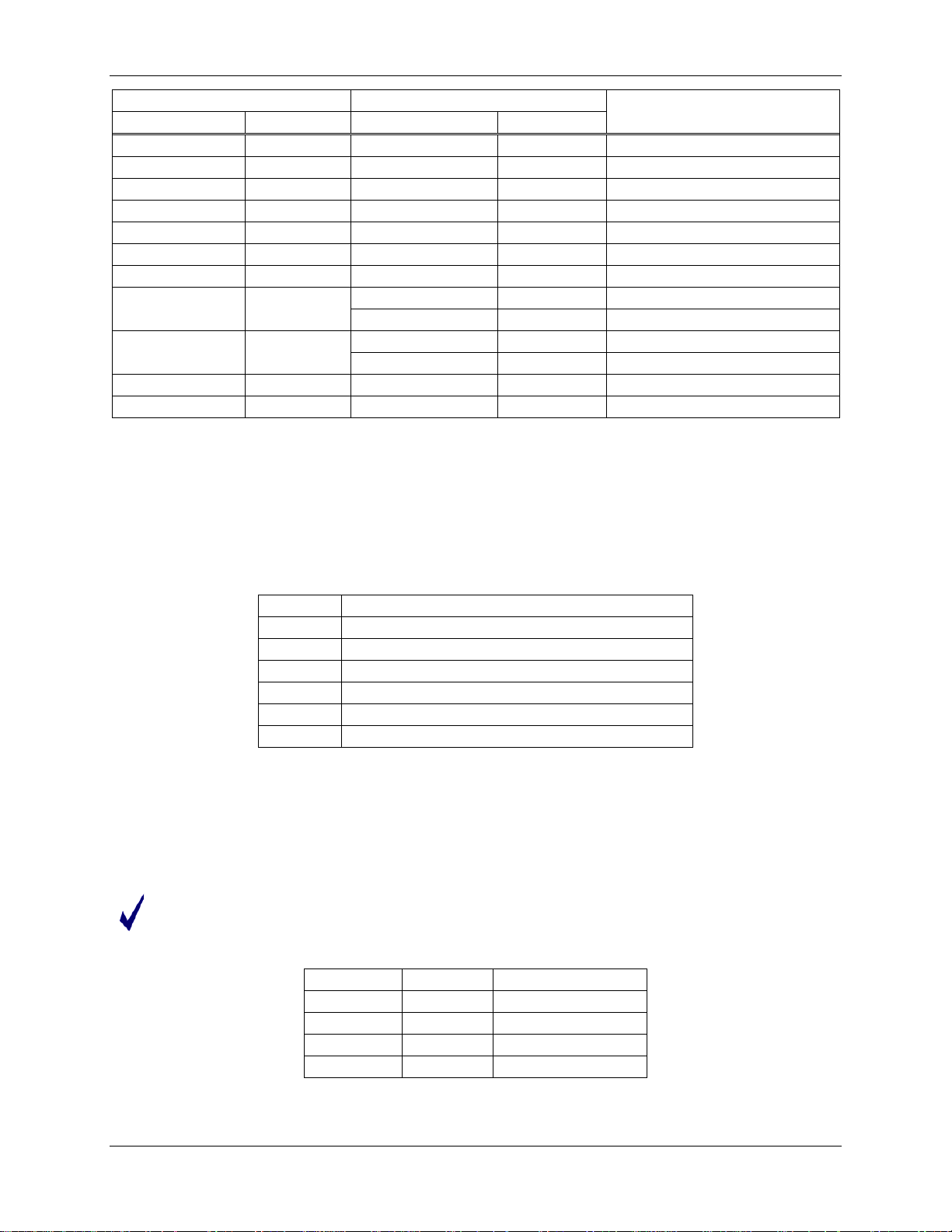
FDS 6531/6532 005 Data Sheet 71M6531D/F-71M6532D/F
Interrupt Enable
Interrupt Flag
Name
Location
Name
Location
EX5
IEX5
EX6
IEX6
EX_RTC
IE_RTC
IEN_WD_NROVF
WD_NROVF_FLAG
IE_FWCOL0
IE_FWCOL1
IE_PLLRISE
IE_PLLFALL
IE_WAKE
IE_PB
Group
Group Members
Interrupt Description
EX4
SFR B8[3]
SFR B8[4]
SFR B8[5]
EX_XFER
2002[0]
2002[1]
20B0[0]
IEN_SPI
EX_FWCOL
EX_PLL
20B0[4]
2007[4]
2007[5]
†
The AUTOWAKE and PB flag bits are shown in Table 31 because they behave similarly to interrupt f l ags,
IEX4
IE_XFER
SPI_FLAG
SFR C0[3] External interrupt 4
SFR C0[4] External interrupt 5
SFR C0[5] External interrupt 6
SFR E8[0] XFER_BUSY interrupt (INT 6)
SFR E8[1] RTC_1SEC interrupt (INT 6)
20B1[0] WDT near overflow (INT 6)
20B1[4] SPI Interface (INT2)
SFR E8[3] FWCOL0 interrupt (INT 2)
SFR E8[2] FWCOL1 interrupt (INT 2)
SFR E8[6] PLL_OK rise interrupt (INT 4)
SFR E8[7] PLL_OK fall interrupt (INT 4)
SFR E8[5] AUTOWAKE flag†
SFR E8[4] PB flag†
even though they are not actually related to an interrupt. These bits are set by hardware when the MPU
wakes from a push button or wake timeout. The bits are res et by writing a zero. Note that the PB flag is
set whenever the PB is pushed, even if the part i s already awake.
Interrupt Priority Level Structure
All interrupt sources are combined in groups, as sh own in Table 32:
Table 32: Interrupt Priority Level Groups
0 External interrupt 0, Serial channel 1 interrupt
1 Timer 0 interrupt, External interrupt 2
2 External interrupt 1, External interrupt 3
3 Timer 1 interrupt, External interrupt 4
4 Serial channel 0 interrupt, External interrupt 5
5 External interrupt 6
Each group of interrupt sources can be programmed individually to one of four priority levels (as shown in
Table 33) by setting or clearing one bit in the SFR interrupt priority register IP0 and one in IP1 (Table 34).
If requests of the same priority level are received simultaneously, an internal polling sequence as shown
in Table 35 determines which request is serviced first.
Changing interrupt priorities while interrupts are enabled can easily cause software defects. It is best
to set the interrupt priority registers only once during initialization before interrupts are enabled.
Table 33: Interrupt Priority Levels
IP1[x] IP0[x]
Priority Level
0 0 Level 0 (lowest)
0 1 Level 1
1 0 Level 2
1 1 Level 3 (highest)
v1.3 © 2005-2010 TERIDIAN Semiconductor Corporation 33
Page 34
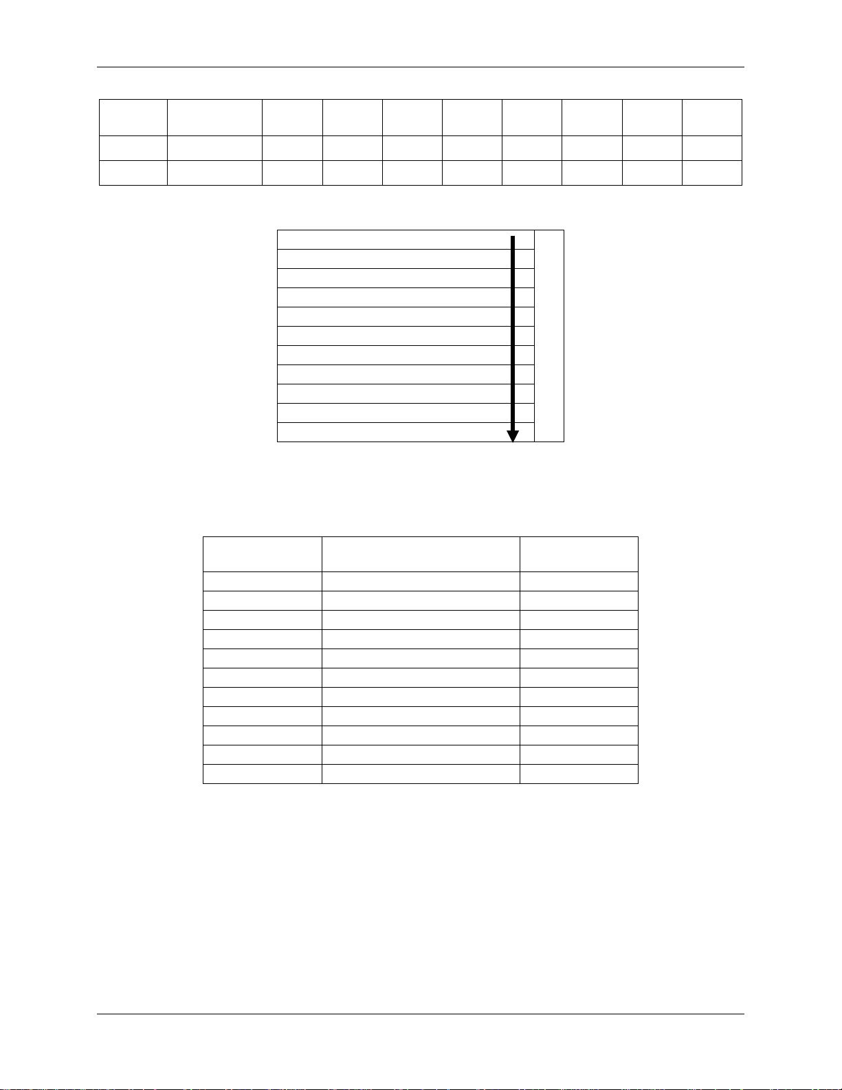
Data Sheet 71M6531D/F-71M6532D/F FDS 6531/6532 005
(LSB)
–
–
–
–
Request Flag
Address
IE0
TF1
IEX2
IEX5
IEX6
Table 34: Interrupt Priority Registers (IP0 and IP1)
Register Address
Bit 7
Bit 6 Bit 5 Bit 4 Bit 3 Bit 2 Bit 1 Bit 0
(MSB)
IP0
SFR 0xA9
IP0[5] IP0[4] IP0[3] IP0[2] IP0[1] IP0[0]
IP1
SFR 0xB9
IP1[5] IP1[4] IP1[3] IP1[2] IP1[1] IP1[0]
Table 35: Interrupt Polling Sequence
External interrupt 0
Serial channel 1 interrupt
Timer 0 interrupt
External interrupt 2
External interrupt 1
External interrupt 3
Timer 1 interrupt
External interrupt 4
Serial channel 0 interrupt
Polling sequence
External interrupt 5
External interrupt 6
Interrupt Sources and Vectors
Table 36 shows the interrupts with their as sociated flags and vector addresses.
Table 36: Interrupt Vectors
Interrupt
Description
Interrupt Vector
External interrupt 0 0x0003
TF0
IE1
Timer 0 interrupt 0x000B
External interrupt 1 0x0013
Timer 1 interrupt 0x001B
RI0/TI0
RI1/TI1
Serial channel 0 interrupt 0x0023
Serial channel 1 interrupt 0x0083
External interrupt 2 0x004B
IEX3
IEX4
External interrupt 3 0x0053
External interrupt 4 0x005B
External interrupt 5 0x0063
External interrupt 6 0x006B
34 © 2005-2010 TERIDIAN Semiconductor Corporation v1.3
Page 35
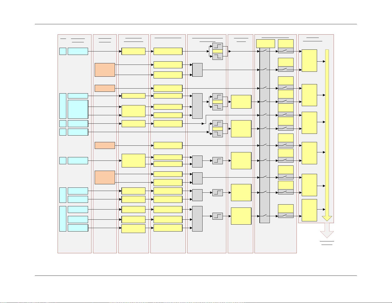
FDS 6531/6532 005 Data Sheet 71M6531D/F-71M6532D/F
TCON.1 (IE0)
Individual
Enable Bits
S1 CON.0 ( RI1)
S1 CON.1 ( TI1)
Individual Flags
Internal
Source
>= 1
TCON.5 (TF0)
TCON.3 (IE1)
TCON.7 (TF1)
S0 CON.0 ( RI0)
S0 CON.0 ( TI0)
>= 1
IRCON.1
(IEX2)
I 2 FR
IRCON.2
(IEX3)
I 3 FR
IRCON.3
(IEX4)
IRCON.4
(IEX5)
IRCON.5
(IEX6)
IEN0.7
(EAL)
IP1.0/
IP0.0
IP1.1/
IP0.1
IP1.2/
IP0.2
IP1.3/
IP0.3
IP1.4/
IP0.4
IP1.5/
IP0.5
Interrupt
Flags
Priority
Assignment
Interrupt
Vector
Polling Sequence
Interrupt Enable
Logic and Polarity
Selection
DIO
Timer 0
Timer 1
CE_BUSY
UART0
EEPROM
XFER_BUSY
RTC_1S
EX_RTC
PLL OK
External
Source
DIO_Rn
DIO_Rn
I2C
>= 1
Flash
Write
Collision
>= 1
IEN2.0
(ES1)
IEN0.1
(ET0)
IEN0.0
(EX0)
IEN1.1
(EX2)
IEN0.2
(EX1)
IEN1.2
(EX3)
IEN0.3
(ET1)
IEN1.3
(EX4)
IEN0.4
(ES0)
IEN1.4
(EX5)
IEN1.5
(EX6)
IE_XFER
IE_RTC
EX_XFER
>= 1
EX_EEX
EX_SPI
IE_EEX
IE_SPI
IT0
IE_FWCOL1
SPI_FLAG
UART1
(optical)
0
2
1
3
4
5
6
No.
Flag=1 means
that an inter-
rupt has oc-
curred and
has not been
cleared
EX0 – EX6 are cleared
automatically when the
hardware vectors to the
interrupt handler
byte received
byte transmitted
overflow occurred
overflow occurred
byte received
byte transmitted
accumulation
cycle completed
PLL status
changed
CE completed code run and
has new status information
DIO status
changed
DIO status
changed
every second
BUSY fell
command
received
SPI I/F
Write attempt, CE
busy
2/2/2009
IE_FWCOL0
DIO
NR_OVF
EX_FWCOL
EX_PLL
IE_PLLRISE
IE_PLLFALL
IEN_SPI
IEN_NR_
WDOVF
WD_NROVF_FLAG
CE code start,
flash write busy
WDT near
overflow
>= 1
MPU-external
sources
MPU-internal
sources
v1.3 © 2005-2010 TERIDIAN Semiconductor Corporation 35
Figure 8: Interrupt Structure
Page 36

Data Sheet 71M6531D/F-71M6532D/F FDS 6531/6532 005
M40MHZ, M26MHZ
÷2 / [1,0]
÷3 / [0,1]
÷4** / [0,0]
MHz
MHz
**
Default state at power-up
1.5 On-Chip Resources
1.5.1 Oscillator
The oscillator of the 71M6531D/F and 71M6532D/F drives a standard 32.768 kHz watch crystal. These
crystals are accurate and do not require a high-current oscillator circuit. The oscillator of the 71M6531D/F
and 71M6532D/F has been designed specific al l y to handle these crystals and is compatible wi th their
high impedance and limited power handling capabilit y.
Oscillator calibration can improve the accuracy of both the RTC and metering. Refer to Section 1.5.3
Real-Time Clock (RTC) for more information.
The oscillator is powered directly and only from VBAT, which therefore must be connected to a DC voltage
source. The oscillator requires approximately 100 nA, which is negligible compared to the internal leakage
of a battery.
The oscillator may appear to work when VBAT is not c onnec ted, bu t this mode o f operat ion is not
recommended.
If VBAT is connected to a drained battery or disco nnected, a battery test that sets BME m ay drain
VBAT’s supply and cause the oscillator to st op. A stopped oscillator may force the device to reset.
Therefore, an unexpected reset during a battery test should be interpreted as a battery failure.
1.5.2 Internal Clocks
Timing for the device is derived from the 32.768 kHz crystal oscillator output. On-chip timing functions
include:
• The MPU clock (CKMPU)
• The emulator clock (2 x CKMPU)
• The clock for the CE (CKCE)
• The clock driving the delta-sigma ADC along with the FIR (CKADC, CKFIR)
• A real time clock (RTC).
The two general-purpose counter/timers contai ned i n the MPU are controlled by CKMPU (see Section
1.4.7 Timers and Counters). Table 37 provides a summary of the available clock functions.
Table 37: Clock System Summary
Clock
Derived
From
MCK Divider / [
CKPLL Crystal 78.6432 MHz
MCK CKPLL 39.3216 MHz
CKCE MCK
4.9152
MHz
9.8304
†
MHz †
78.6432
26.2144
MHz
6.5536MHz 4.9152 MHz off
]
78.6432
19.6608
MHz
Brownout
Mode
off
112 kHz
CKADC / CKFIR MCK 4.9152 MHz 6.5536 MHz 4.9152 MHz 28 kHz
CKMPU maximum MCK 9.8304 MHz
***
6.5536 MHz
***
4.9152 MHz
***
28 kHz
CK32 MCK 32.768 kHz 32.768 kHz 32.768 kHz
***
The maximum CKMPU frequency. CKMPU can be reduced from this rate using MPU_DIV[2:0].
†
CKCE = 9.8304 MHz when CE10MHZ is set, 4.9152 MHz otherwise.
The master clock, MCK, is generated by an on-chi p PLL that multiplies the oscillator output frequency
(CK32) by 2400 to provide approximately 80 M Hz ( 78.6432 MHz ). A divider controlled by the I/O RAM
bits M40MHZ and M26MHZ permits scaling of MCK by ½, ⅓ and ¼. All other clocks are derived from this
scaled MCK output (making them multiples of 32768 Hz), and the clock skew is matched so that the rising
edges of CKADC, CKCE, CK32 and CKMPU are aligned.
36 © 2005-2010 TERIDIAN Semiconductor Corporation v1.3
Page 37

FDS 6531/6532 005 Data Sheet 71M6531D/F-71M6532D/F
pF
ADJRTCA
C
ADJ
5.16
128
_
⋅=
The PLL generates a 2x emulator clock which is controlled by the ECK_DIS bit. Since clock noise from
this feature may disturb the ADC, it is recommended that this option be avoided when possible.
The MPU clock frequency CKMPU is determined by another divider controlled by the I/O RA M field
MPU_DIV[2:0] and can be set to MCK/2
(
MPU_DIV
+2)
Hz where MPU_DIV[2:0] varies from 0 to 6. The circuit
also generates the 2 x CKMPU clock for use by the em ul ator. The emulator clock is not generated when
ECK_DIS is asserted.
During a power-on reset, [M40MHZ, M26MHZ] defaults to [0,0] and the MCK divider is set to divide by 4.
When [M40MHZ, M26MHZ] = [1,0], the CE clock frequency may be set to ~5 MHz (4.9152 MHz) or ~10
MHz (9.8304 MHz), using the I/O RAM register CE10MHZ. In this mode, the ADC and FIR clock frequencies remain at ~ 5 MHz. When [M40MHZ, M26MHZ] = [0,1], the CE, ADC, FIR and MPU clock frequencies are shifted to ~ 6.6 MHz (6.5536 MHz). This increases t he A DC sample rate by 33%.
CE codes are tailored to particular clock frequenc ies . Chang ing the c lock frequency for a
particular CE code may render it unusable.
In sleep mode, the M40MHZ and M26MHZ inputs to the clock generator are forced low. In brownout
mode, the clocks are derived from the crystal oscillator and the clock frequencies are scaled by 7/8.
1.5.3 Real-Time Clock (RTC)
The RTC is driven directly by the crystal oscillator. It is powered by the net RTC_NV (battery-backed up
supply). The RTC consists of a counter chain and output registers. The counter chain consists of registers
for seconds, minutes, hours, day of week, day of month, month and year. The RTC i s capable of
processing leap years. Each counter has its own output register. Whenever the MPU reads the seconds
register, all other output registers are automatically updated. Since the RTC clock (RTCLK) is not coherent
to the MPU clock, the MPU must read the secon ds register until two consecutive reads are the same (this
requires either 2 or 3 reads). At this point, all RTC output registers will have the correct time. Regardless
of the MPU clock speed, RTC reads require one wait state.
RTC time is set by writing to the registers RTC_SEC[5:0] through RTC_YR. Each write operation must be
preceded by a write operation to the WE register in I/O RAM. The value written to the WE register is
unimportant.
Time adjustments are written to the RTCA_ADJ[6:0], PREG[16:0] and QREG[1:0] registers. Updates to
PREG[16:0] and QREG[1:0] must occur after the one second interrupt and must be finished before reaching
the next one second boundary. The new values are l oaded into the counters at the next one second
boundary.
PREG[16:0] and QREG[1:0] are separate registers in the device hardware, but the bits are 16-bit contiguous
so the MPU firmware can treat them as a single register. A single binary number can be calculated and
then loaded into them at the same time.
The 71M6531D/F and 71M6532D/F have two rate adjustment mechanisms. The first is an analo g rate
adjustment, using RTCA_ADJ[6:0], which trims the crystal load capacitance. Setting RTCA_ADJ[6:0] to 00
minimizes the load capacitance, maximizing the oscillator frequency. Setting RTCA_ADJ[6:0] to 0x3F
maximizes the load capacitanc e , mi ni mizing the oscillator frequency. The adjustable capacitance is
approximately:
The maximum adjustment range is approximately-12 ppm to +22ppm. The precise amount of adjustment
will depend on the crys tal p r op erties. The adjustment may occur at any time and the resulting clock
frequency can be measured over a one-second interval.
The second rate adjustment is a digital rate adju st using PREG[16:0] and QREG[1:0], which can be used
to adjust the clock rate up to ± 988 ppm, with a resolution of 3.8 ppm. Updates must occur after a one
second interrupt and must finish before the next one second boundary. The rate adjustment will be
implemented starting at the next one second boundary. Since the LSB results in an adjustment every
four seconds, the frequency should be measured over an interval that is a multiple of four seconds.
v1.3 © 2005-2010 TERIDIAN Semiconductor Corporation 37
Page 38

Data Sheet 71M6531D/F-71M6532D/F FDS 6531/6532 005
+
⋅∆+
⋅
=+⋅
−
5.0
101
832768
4
6
floorQREGPREG
To adjust the clock rate using the digital rate adjust, the appropriate values must be written to PREG[16:0]
and QREG[1:0]. The default frequency is 32,768 RTCLK cycles per second. To shift the clock frequency
by ∆ ppm, calculate PREG[16:0] and QREG[1:0] using the following equation:
For example, for a shift of -988 ppm, 4⋅PREG + QREG = 262403 = 0x40103. PREG[16:0] = 0x10040 and
QREG[1:0] = 0x03. The default values of PREG[16:0] and QREG[1:0], corresponding to zero adjustment,
are 0x10000 and 0x0, respectively.
The RTC timing may be observed on the TMUXOUT pin by setting TMUX[4:0] to 0x10 or 0x11.
Default values for RTCA_ADJ, PREG[16:0] and QREG[1:0] should be nominal values, at the center of
the adjustment range. Extreme values (zero for example) can cause incorrect operation.
If the crystal temperature coefficient is known, the MPU can integrate temperature and correct the RTC
time as necessary.
The sub-second register of the RTC, SUBSEC, can be read by the MPU after the one second interrupt and
before reaching the next one second boundary. SUBSEC contains the count remaining, in 1/256 second
nominal clock periods, until the next one second boundary. When the RST_SUBSEC bit is written, the
SUBSEC counter is restarted. Reading and resetting the sub-second counter can be used as part of an
algorithm to accurately set the RTC.
When setting the RTC_SEC register, it is important to take into account that the associated write operation
will be performed only in the next second boundary.
1.5.4 Temperature Sensor
The device includes an on-chip temperature sensor for determining the temperature of the bandgap
reference. If automatic temperature measurement is not performed by selecting CHOP_E[1:0] = 00, the
MPU may request an alternate multiplexer frame containing the temperature sensor output by asserting
MUX_ALT. The primary use of the temperat ure da ta is to de termine the magn itude of com pensa tion
required to offset the t herm al drift in t he sy stem (see Section 3.4 Temperature Compensation).
1.5.5 Physical Memory
Flash Memory
The 71M6531D and 71M6532D include 128 KB of on-chip flash memory. The 71M653 1F and 71M6532F
offer 256 KB of flash memory. The flash memory primarily contains MPU and CE program code. It also
contains images of the CE and MPU data in RAM, as wel l as of I/O RAM. On power-up, before enabling
the CE, the MPU copies these images to their respective locations.
The flash memory is segmented into individually erasable pages that contain 1024 bytes.
Flash space allocated for the CE program is limited to 4096 16-bit words (8 KB). The CE pro gram m ust
begin on a 1-KB boundary of the flash address spac e. The CE_LCTN[7:0] word defines which 1-KB
boundary contains the CE code. Thus, the first CE instruction is located at 1024*CE_LCTN[7:0].
Flash Write Procedures
The MPU may write to the flash memory. Thi s is one of the non-volatile storage options available t o the
user in addition to external EEPROM.
FLSH_PWE (flash program write enable) differentiates 80515 data store instructions (MOVX@DPTR,A)
between Flash and XRAM write operations. T hi s bit must be cleared by the MPU after each by te write
operation. Write operations to this bit are inhibi ted when interrupts are enabled.
The MPU cannot write to flash while the CE is executing its code from flash. Two interrupts warn of collisions
between the MPU firmware and the CE timing. If a flash write operation is attempted while the CE i s
busy, the flash write will not execute and the FWC OL0 interrupt will be issued. If a flash write is still in
progress when the CE would otherwise begin a code pass, the code pass is skipped, the write operation
is completed, and the FWCOL1 interrupt is iss ued.
38 © 2005-2010 TERIDIAN Semiconductor Corporation v1.3
Page 39

FDS 6531/6532 005 Data Sheet 71M6531D/F-71M6532D/F
The simplest flash write procedure disables the CE during the write operation and interpolates the metering
measurements. However, this results in the los s of at least one second of data, because the CE has t o
resynchronize with the mains voltage.
There is a brief guaranteed interval (typically 1/32768 s) between CE executions which occurs 2520 times
per second. The start of the interval can be detect ed with the CE_BUSY interrupt which occurs on the
falling edge of CE_BUSY (an internal signal m easurable from TMUXOUT). However, this guaranteed idle
time (30.5 µs) is too short to write a byte whic h takes 42 µs or to erase a page of flash memory which
takes at least 20 ms. Some CE code has substantially lo nger idle times, but in those c ases, firmware
interrupt latencies can easily consume the available write time. If a flash write fails in this scheme, the
failure can be detected with the FWCOL0 or FWCOL1 interrupt and the write can be retried.
It is practical to pre-erase pages, disable interrupts and poll the CE_BUSY interrupt flag, IRCON[2]. This
method avoids problems with interrupt latency, but can still result in a write failure if the CE code takes to
much time. As mentioned above, polling FWCOL0 and FWCOL1 can detect write failures. However, the
speed in a polling write is only 2520 bytes per se cond and the firmware cannot respond to interrupt s.
As an alternative to using flash, a small EEPROM can store data without compromises. EEPROM interfaces
are included in the device.
Updating Individual Bytes in Flash Memory
The original state of a flash byte is 0xFF (all one s). Once a value other than 0xFF is written to a flash
memory cell, overwriting with a different value usuall y requires that the cell be erased first. Since cel l s
cannot be erased individually, the page has to be c opied to RAM, followed by a page erase. After this,
the page can be updated in RAM and then written back to the flash memory.
Flash Erase Procedures
Flash erasure is initiated by writing a specific data pattern to specific SFR registers in the proper sequence.
These special patte rn/sequ ence requi rement s prev ent i nadve rtent erasur e of t he fla sh mem ory.
The mass erase sequence is:
1. Write 1 to the FLSH_MEEN bit (SFR 0xB2[1]).
2. Write pattern 0xAA to FLSH_ERASE (SFR 0x94).
The mass erase cycle can only be initiated when the ICE port is enabled.
The page erase sequence is:
1. Write the page address to FLSH_PGADR[5:0] (SFR 0xB7[7:1]).
2. Write pattern 0x55 to FLSH_ERASE (SFR 0x94).
Bank-Switching:
The program memory of the 71M6531 consists of a fixed lower bank of 32 KB addressable at 0x0000 to
0x7FFF plus an upper bank area of 32 KB, addres sable at 0x8000 to 0xFFFF. The upper 32 KB space is
banked using the I/O RAM FL_BANK register as follows:
• The 71M6531D provides 4 banks of 32 KB each selected by FL_BANK[1:0]. Note that when
FL_BANK[1:0] = 00, the upper bank is the same as the lower bank.
• The 71M6531F and 71M6532D/F provide 8 banks of 32 KB each selected by FL_BANK[2:0].
Table 38 illustrates the bank switching mechanism.
v1.3 © 2005-2010 TERIDIAN Semiconductor Corporation 39
Page 40

Data Sheet 71M6531D/F-71M6532D/F FDS 6531/6532 005
Bank (0x000-0x7FFF)
Bank (0x8000-0xFFFF)
Table 38: Bank Switching with FL_BANK[2:0]
71M6531D
FL_BANK [1:0]
000 000
001 001 0x8000-0xFFFF
010 010 0x10000-0x17FFF
011 011 0x18000-0x1FFFF
100 0x20000-0x217FF
Program Security
When enabled, the security feature limits the ICE to global flash erase operations only. All other ICE
operations are blocked. This guarantees t he security of the user’s MPU and CE program code. Security
should be enabled by MPU code that is executed during the pre-boot interval (60 CKMPU cycles before
the primary boot sequence begins). Once security i s enabled, the only way to disable it is to perform a
global erase of the flash, followed by a chip res et.
The first 60 cycles of the MPU boot code are called the pre-boot phase because during this phase the
ICE is inhibited. A read-only status bit, PREBOOT, identifies these cycles to the MPU. Upon completion
of pre-boot, the ICE can be enabled and is permitt ed to take control of the MPU.
71M653XF
FL_BANK [2:0]
101 0x28000-0x2FFFF
110 0x30000-0x37FFF
111 0x38000-0x3FFFF
Address Range for Lower
0x0000-0x7FFF
Address Range for Upper
0x0000-0x7FFF
The security enable bit, SECURE, is reset whenever the chip is reset. Hardware associated with the bit
permits only ones to be written to it. Thus, pre-boot c ode m ay set SECURE to enable the security feature
but may not reset it. Once SECURE is set, the pre-boot code is protected and no external read of program
code is possible
Specifically, when SECURE is set, the following applies:
• The ICE is limited to bulk flash erase only.
• Page zero of flash memory, the preferred locat i on for the user’s pre-boot code, may not be
page-erased by either MPU or ICE. Page zero may only be erased with global flash erase.
• Write operations to page zero, whether by MPU or I CE are inhibited.
MPU/CE RAM:
The 71M6531D/F and 71M6532D/F include 4 KB of static RAM memory on-chip (XRAM) plus 256-bytes
of internal RAM in the MPU core. The 4 KB of static RAM are used for data storage for MPU and CE
operations.
1.5.6 Optical Interface
The device includes an interface to implement an IR/optical port. The pin OPT_TX is designed t o di rectly
drive an external LED for transmitting data on an optical link. The pin OPT_RX has the same threshold
as the RX pin, but can also be used to sense the input from an external photo detector used as the receiver
for the optical link. OPT_TX and OPT_RX are con nected to a dedicated UART port (UART1).
The OPT_TX and OPT_RX pins can be inverted with configuration bits OPT_TXINV and OPT_RXINV,
respectively. Additionally, the OPT_TX output may be modulated at 38 kHz. Modulation is available when
system power is present (i.e. not in BROWNOUT mode). The OPT_TXMOD bit enables modulation. Duty
cycle is controlled by OPT_FDC[1:0], which can select 50%, 25%, 12.5% and 6.25% duty cycle. 6.25% duty
cycle means OPT_TX is low for 6.25% of the period. Figure 9 illustrates the OPT_TX generator.
When not needed for the optical UART, the OP T_T X pin can alternatively be configured as DIO2,
WPULSE, or VARPULSE. The configuration bits are OPT_TXE[1:0]. Likewise, OPT_RX can alternately
be configured as DIO1. Its control is OPT_RXDIS.
40 © 2005-2010 TERIDIAN Semiconductor Corporation v1.3
Page 41
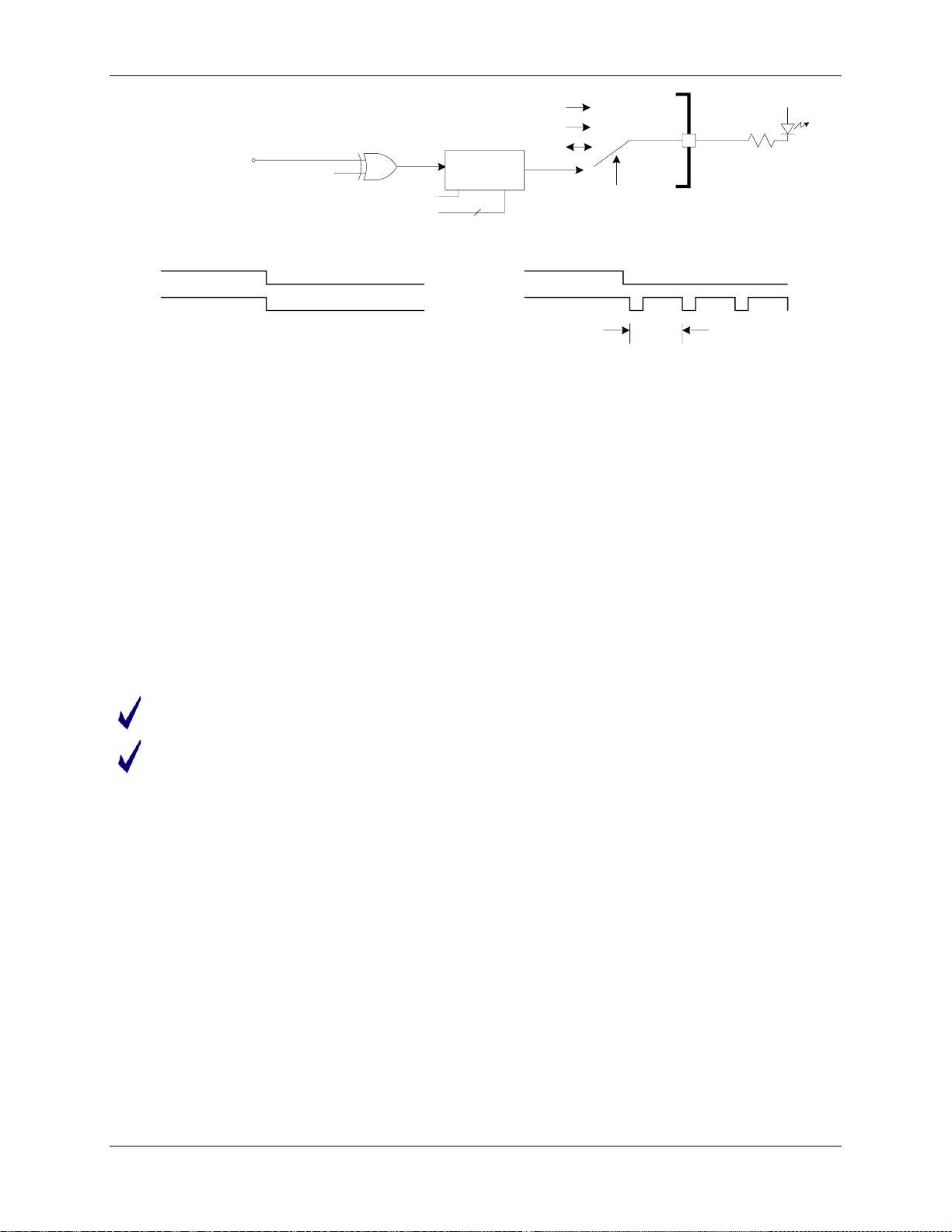
FDS 6531/6532 005 Data Sheet 71M6531D/F-71M6532D/F
B
A
OPT_TXMOD = 0
OPT_TXMOD = 1,
OPT_FDC = 2 (25%)
B
A
1/38kHz
OPT_TXINV
from
OPT_TX UART
MOD
EN DUTY
OPT_TX
OPT_TXMOD
OPT_FDC
OPT_TXE[1:0]
1
2
V3P3
Internal
A
B
0
2
3
DIO2
WPULSE
VARPULSE
Figure 9: Optical Interface
1.5.7 Digital I/O – 71M6531D/F
The 71M6531D/F includes up to 22 pins of general-purpose digital I/O. These pins are compatible with 5 V
inputs (no current limiting resistors are neede d). The Digital I/O pins can be categorized as follows:
• Dedicated DIO pins (1 pi n): PB
• DIO/LCD segment pi ns (a total of 19 pins):
o DIO4/SEG24 - DIO15/SEG35 (12 pins)
o DIO17/SEG37 (1 pin)
o DIO28/SEG48 – DIO29/SEG49 (2 pins)
o DIO43/SEG63 - DIO46/SEG66 (4 pins)
• DIO pins combined with other functions (2 pins): DIO2/OPT_TX, DIO1/OPT_RX
The pins DIO4/SEG24 through DIO46/SEG66 are configured by the LCD_BITMAP registers to be DIO o r
segment pins. A one in LCD_BITMAP defines the pin as a L CD segment output, a zero makes the pin a
DIO pin. Pins configured as LCD pins are controlled with the LCD_SEGnn registers. Pins configured as
DIO can be defined independently as an input or output with the DIO_DIR bits (see Table 45).
Write operations to a disabled DIO are not ignored. Write operations are registered, but do not affect
the pin, or the result of a read operation on the pin, un til it becomes a DIO output.
DIO2/OPT_TX will be an active TX output pin at power up (OPT_TXE[1:0] = 00).
A 3-bit configuration word, I/O RAM field DIO_Rx[2:0] (0x2009[2:0] through 0x200E[6:4]), can be used for
certain pins (when configured as DIO) to indiv idual l y assign an internal resource such as an interrupt or a
timer control (see Table 46 for DIO pins avail abl e for this option). This way, DIO pins can be tracked
even if they are configured as outputs.
Table 39 to Table 41 lists the direction registers and configurability associated with each group of DIO pins.
v1.3 © 2005-2010 TERIDIAN Semiconductor Corporation 41
Page 42
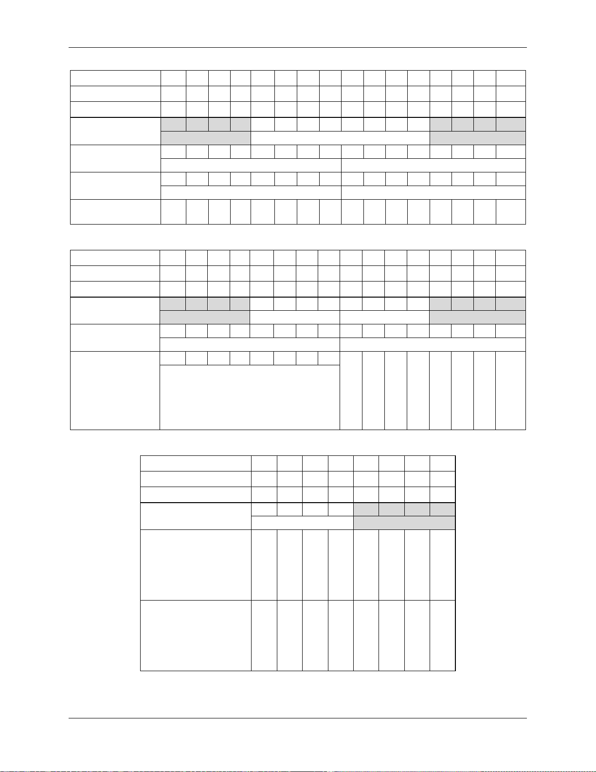
Data Sheet 71M6531D/F-71M6532D/F FDS 6531/6532 005
Table 39: Data/Direction Registers and Internal Resources for DIO 1-15 (71M6531D/F)
DIO PB 1 2
LCD Segment
– – – –
Pin number 65 60 3
Configuration (DIO
– – – – 0 1 2 3 4 5 6 7 0 1 2 3
or LCD segment)
Data Register
Direction Register
Internal Resources
Configurable
0 1 2 – 4 5 6 7 0 1 2 3 4 5 6 7
– 1 2 – 4 5 6 7 0 1 2 3 4 5 6 7
– – – – Y Y Y Y Y Y Y Y – – – –
DIO0 = P0 (SFR 0x80) DIO1 = P1 (SFR 0x90)
DIO_DIR0 (SFR 0xA2) DIO_DIR1 (SFR 0x91)
–
4 5 6 7 8 9 10 11 12 13 14 15
24 25 26 27 28 29 30 31 32 33 34 35
–
39 40 41 42 43 44 45 46 68 30 21 22
LCD_BITMAP[31:24] LCD_BITMAP[39:32]
Table 40: Data/Direction Registers and Internal Resources for DIO 17-29 (7 1M 6531D/F)
DIO
LCD Segment
Pin number
Configuration (DIO
or LCD segment)
Data Register
–
–
–
– 5 – – – – – – – – – – 0 1 – –
LCD_BITMAP[39:32]
– 1 – – – – – – – – – – 4 5 – –
– – – – – – – – – –
17
– – – – – – – – – –
37
– – – – – – – – – –
13
28 29
48 49
47 24
LCD_BITMAP[55:48]
DIO2 = P2 (SFR 0xA0) DIO3 = P3 (SFR 0xB0)
– –
– –
– –
– 1 – – – – – –
Direction Register
0 = input,
1 = output
DIO_DIR2 (SFR 0xA1)
Table 41: Data/Direction Registers and Internal Resources for DIO 43-46 (71M 6531D/F)
DIO
LCD Segment
Pin number
Configuration (DIO or
LCD segment)
– – –
– – –
– – –
– – – 7
43 44 45 46
63 64 65 66
29 23 28 5
0 1 2 –
LCD_BITMAP[63:56] LCD_BITMAP[64:71]
Data Register – – –
LCD_SEG63[0]
LCD_SEG64[0]
LCD_SEG65[0]
LCD_SEG66[0]
Direction Register
0 = input, 1 = output
– – –
–
–
–
–
–
LCD_SEG48[3]
LCD_SEG49[3]
LCD_SEG63[3]
LCD_SEG64[3]
LCD_SEG65[3]
LCD_SEG66[3]
42 © 2005-2010 TERIDIAN Semiconductor Corporation v1.3
Page 43
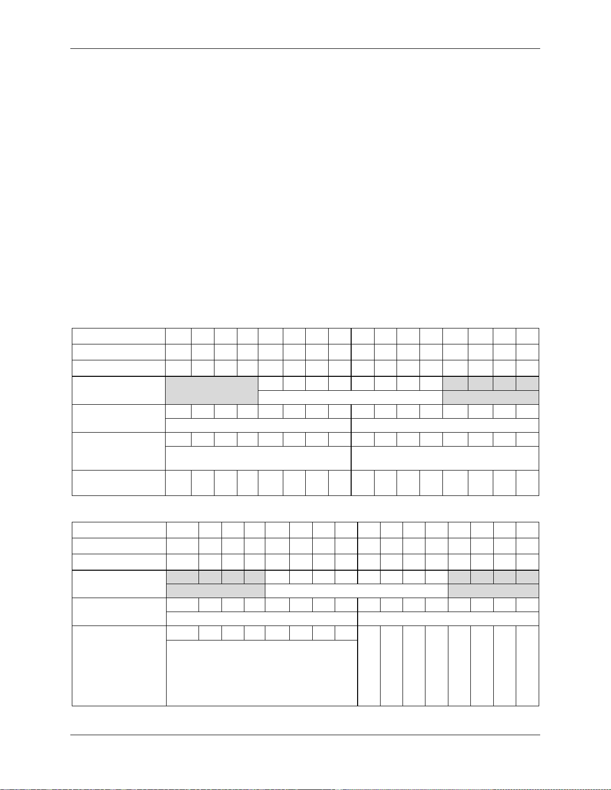
FDS 6531/6532 005 Data Sheet 71M6531D/F-71M6532D/F
1.5.8 Digital I/O – 71M6532D/F
The 71M6532D/F includes up to 43 pins of general-purpose digital I/O. These pins are compatible with 5 V
inputs (no current limiting resistors are neede d). The Digital I/O pins can be categorized as follows:
• Dedicated DIO pins (4 pins):
o DIO3
o DIO56 – DIO58 (3 pins)
• DIO/LCD segment pi ns (a total of 37 pins):
o DIO4/SEG24 – DIO27/SEG47 (24 pins)
o DIO29/SEG49, DIO30/SEG50 (2 pins)
o DIO40/SEG60 – DIO45/SEG65 (6 pins)
o DIO47/SEG67 – DIO51/SEG71 (5 pins)
• DIO pins combined with other functions (2 pins): DIO2/OPT_TX, DI O 1/OPT_RX
On reset or power-up, all DIO pins are inputs until they are configured for the desired direction und er
MPU control. The pin function can be configured by the I/O RAM bits LCD_BITMAPn. Setting
LCD_BITMAPn = 1 configures the pin for LCD, set ting LCD_BITMAPn = 0 configures it for DIO. Once a
pin is configured as DIO, it can be configured independently as an input or output with the DIO_DIR bits
or the LCD_SEGn registers. Input and output data are written to or read fro m the pins using SFR registers
P0, P1, and P2. Table 42 to Table 44 shows the DIO pins with their configuration, direction cont rol and
data registers.
Table 42: Data/Direction Registers and Internal Resources for DIO 1-15 (71M6532D/F)
DIO PB 1 2 3 4 5 6 7 8 9 10 11 12 13 14 15
LCD Segment – – – – 24 25 26 27 28 29 30 31 32 33 34 35
Pin number 92 87 3 17 60 61 62 63 67 68 69 70 100 44 29 30
Configuration (DIO
or LCD segment)
Data Register
Direction Register
0 = input,
1 = output
Internal Resources
Configurable
Always DIO
0 1 2 3 4 5 6 7 0 1 2 3 4 5 6 7
DIO0 = P0 (SFR 0x80) DIO1 = P1 (SFR 0x90)
– 1 2 3 4 5 6 7 0 1 2 3 4 5 6 7
DIO_DIR0 (SFR 0xA2) DIO_DIR1 (SFR 0x91)
Y Y Y Y Y Y Y Y Y Y Y Y – – – –
0 1 2 3 4 5 6 7 0 1 2 3
LCD_BITMAP[31:24] LCD_BITMAP[39:32]
Table 43: Data/Direction Registers and Internal Resources for DIO 16-30 (71M 6532D/F)
DIO 16 17 18 19 20 21 22 23 24 25 26 27 – 29 30 –
LCD Segment 36 37 18 39 40 41 42 43 44 45 46 47 – 49 50 –
Pin number 33 12 13 64 65 66 93 54 46 43 42 41 – 32 35
Configuration (DIO
or LCD segment)
Data Register
4 5 6 7 0 1 2 3 – – – – – 1 2 –
LCD_BITMAP[39:32] LCD_BITMAP[47:40] LCD_BITMAP[55:48]
0 1 2 3 4 5 6 7 0 1 2 3 – 5 6 –
DIO2 = P2 (SFR 0xA0) DIO3 = P3 (SFR 0xB0)
– 1 – 3 4 5 – –
Direction Register
0 = input,
1 = output
DIO_DIR2 (SFR 0xA1)
– – – – –
LCD_SEG49[3]
–
LCD_SEG50[3]
v1.3 © 2005-2010 TERIDIAN Semiconductor Corporation 43
Page 44
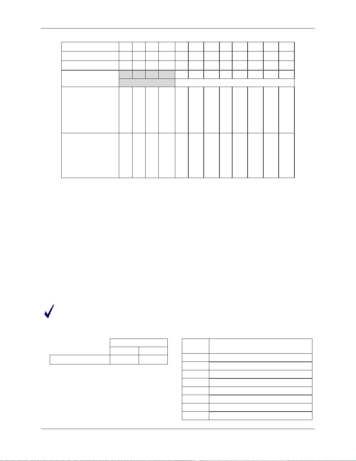
Data Sheet 71M6531D/F-71M6532D/F FDS 6531/6532 005
[n]
0
1
Table 44: Data/Direction Registers and Internal Resources for DIO 40-51 (71M6532D/F)
DIO 40 41 42 43 44 45 – 47 48 49 50 51
LCD Segment 60 61 62 63 64 65 – 67 68 69 70 71
Pin number 95 97 98 40 31 38 – 22 23 24 25 50
Configuration (DIO
or LCD segment)
4 5 6 7 0 1 – 3 4 5 6 7
LCD_BITMAP[63:56] LCD_BITMAP[71:64]
Data Register
LCD_SEG60[0]
LCD_SEG61[0]
LCD_SEG62[0]
LCD_SEG63[0]
LCD_SEG64[0]
Direction Register
0 = input,
1 = output
LCD_SEG60[0]
LCD_SEG61[0]
LCD_SEG62[0]
LCD_SEG63[0]
LCD_SEG64[3]
DIO24 and higher do not have SFR registers for direction control. DIO40 and higher do not have SFR
registers for data access. The direction control of these pins is achieved with the LCD_SEGn[3] bits and
data access is controlled with the LCD_SEGn[0] bits in I/O RAM.
DIO56 through DIO58 are dedicated DIO pins. They are controlled with DIO_DIR56[7] through
DIO_DIR58[7] and with DIO_56[4] through DIO_58[4] in I/O RAM.
–
LCD_SEG65[0]
–
LCD_SEG65[3]
LCD_SEG67[0]
LCD_SEG68[0]
LCD_SEG69[0]
LCD_SEG70[0]
LCD_SEG71[0]
LCD_SEG67[3]
LCD_SEG68[3]
LCD_SEG69[3]
LCD_SEG70[3]
LCD_SEG71[3]
1.5.9 Digital IO – Common Characteristics for 71M6531D/F and 71M6532D/F
On reset or power-up, all DIO pins are inputs until they are configured for the desired direction under
MPU control. The pin function can be configured by the I/O RAM bits LCD_BITMAPn. Setting
LCD_BITMAPn = 1 configures the pin for LCD, set ting LCD_BITMAPn = 0 configures it for DIO. Once a
pin is configured as DIO, it can be configured independently as an input or output with the DIO_DIR bits
or the LCD_SEGn registers. Input and output data are written to or read fro m the pins using SFR registers
P0, P1, and P2.
DIO24 and higher do not have SFR registers for direction control. DIO40 and higher do not have SFR
registers for data access. The direction control of these pins is achieved with the LCD_SEGn[3] registers
and data access is controlled with the LCD_SEGn[0] registers in I/O RAM.
Since the control for DIO24 through DIO5 1 is shared with the control for LCD segments, the firmware
must take care not to disturb the DIO pins when accessing the LCD segm ents a nd vi ce ver sa. U sually,
this requires reading the I/O RAM register, applying a mask and writing back the modified byte.
Table 45: DIO_DIR Control Bit
DIO_DIR
DIO Pin n Function Input Output
44 © 2005-2010 TERIDIAN Semiconductor Corporation v1.3
Table 46: Selectable Control using DIO_DIR Bits
DIO_R
Value
Resource Selected for DIO Pin
0 None
1 Reserved
2 T0 (counter 0 clock)
3 T1 (counter 1 clock)
4 High priority I/O interrupt (INT0 ri sing)
5 Low priority I/O interrupt (INT1 rising)
6 High priority I/O interrupt (INT0 fal l ing)
7 Low priority I/O interrupt (INT1 falling)
Page 45
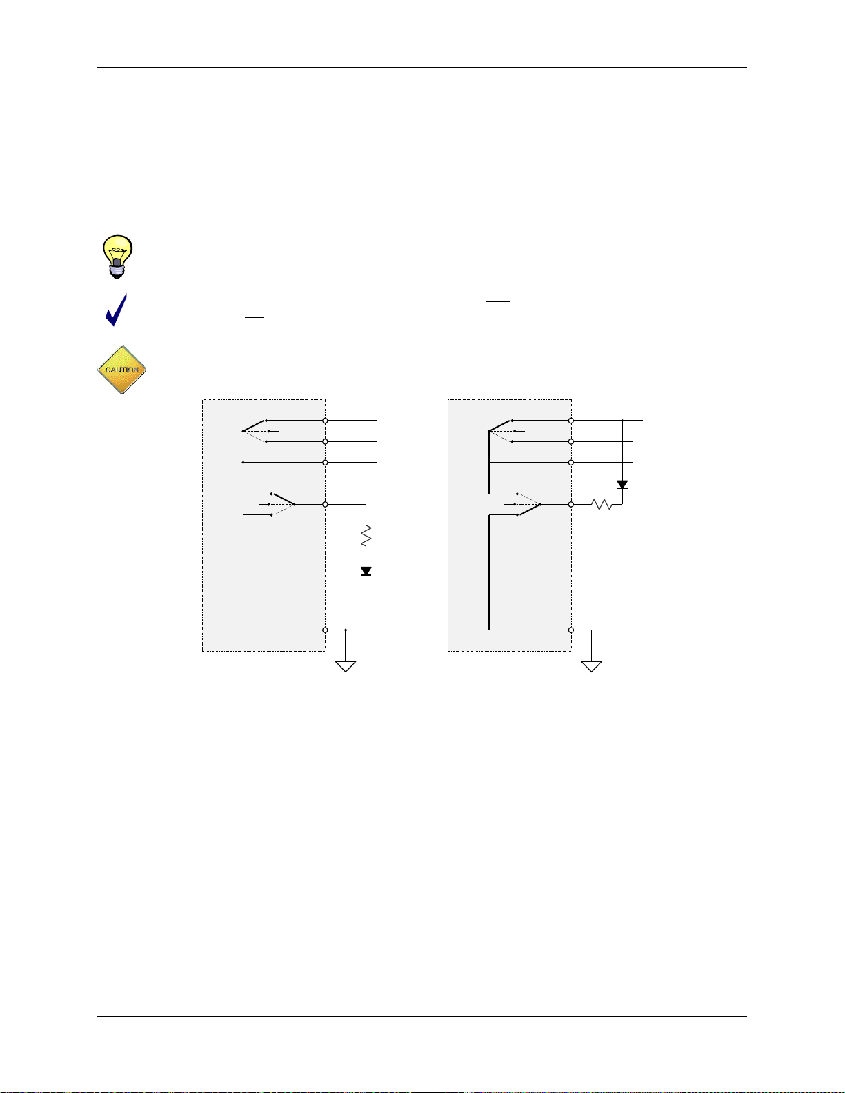
FDS 6531/6532 005 Data Sheet 71M6531D/F-71M6532D/F
V3P3SYS
VBAT
V3P3D
DIO
GNDD
MISSION
BROWNOUT
LCD/SLEEP
LOW
HIGH
HIGH-Z
V3P3SYS
VBAT
V3P3D
DIO
GNDD
MISSION
BROWNOUT
LCD/SLEEP
LOW
HIGH
HIGH-Z
Additionally, if DIO6 and DIO7 are configured as D IO and d efined as ou tputs, the y can be used as
dedicated pulse outputs (WPULSE = DIO6, VARPULSE = DIO7) using the DIO_PW and DIO_PV bits. In
this case, DIO6 and DIO7 are under CE control. DIO4 and DIO5 can be configured to implement the
EEPROM Interface.
The PB pin is a dedicated digital input. In addition, if the optical UART is not used, OPT_TX and OPT_RX
can be configured as dedicated DIO pins, DIO1 and DIO2, respectively (see Section 1.5.6 Optical Interface).
The internal control resources selectable for the DIO pins are listed in Table 46. If more than one input i s
connected to the same resource, the resources are combined using a logical OR.
Tracking DIO pins configured as outputs is useful for pulse counting without external hardware.
Either the interrupts or the counter/timer clocks can be used to count pulses on the pulse outputs
or interrupts on the CE’s power failure output.
the current into GNDD (as shown in
When driving LEDs, relay coils etc., the DIO pins should
Figure 10
, right), not Figure 10 source it from V3P3D (as shown in , left). This is due to the resis-
sink
tance of the internal switch that connects V3P3D to either V3P3SYS or VBAT.
Sourcing current into or out of DIO pins other than the PB pin, for e xample with pull-up or pulldown resistors, should be avoided. Violating t hi s rule will lead to increased quiescent current in
sleep and LCD modes.
Figure 10: Connecting an External Load to DIO Pins
1.5.10 LCD Drivers – 71M6531D/F
The 71M6531 contains a total of 39 dedicated and multiplexed LCD drivers which are grouped as follows:
• 11 dedicated LCD segment drivers – always available
• 3 drivers multiplexed with the ICE interface (E_TCLK, E_RST, E_RXTX) – available in normal operation
mode (when not emulating)
• 2 driver multiplexed with auxiliary signals MUX_SYNC and CKTEST (SEG7, SEG19) – available
when not used for test
• 4 drivers multiplexed with the SPI port (PCLK, PSDO, PCSZ, PSDI)
• 19 multi-use pins described in Section 1.5.7 Digital I/O – 71M6531D/F.
• 4 common drivers for multiplexing (25%, 33%, 50%, or 100% duty cycle) – always available
With a minimum of 1 6 drive r pin s alway s avail able and a total of 39 d river pins i n the maxim um co nfiguration,
the device is capable of driving between 64 to 156 pixels of LCD display with 25% duty cycle. At eight pixels
per digit, this corresponds to 8 to 19 digits. At 33% duty cycle, 48 to 117 pixels can be driven.
For each multi-use pin, the corresponding LCD_BITMAP[] bit (see Section 1.5.7 Digital I/O – 71M6531D/F),
is used to select the pin for DIO or LCD operation. The mappi ng of the LCD_BITMAP[] bits is specified in
v1.3 © 2005-2010 TERIDIAN Semiconductor Corporation 45
Page 46

Data Sheet 71M6531D/F-71M6532D/F FDS 6531/6532 005
Section 4.1 I/O RAM and SFR Map – Functional Order. The LCD drivers are supported by the four common
pins (COM0 – COM3).
1.5.11 LCD Drivers – 71M6532D/F
The 71M6532D/F contains a total of 67 dedicated and multiplexed LCD drivers, which are grouped a s
follows:
• 15 dedicated LCD segment drivers (SEG0 to SEG2, SEG8, SEG12 - SEG18, SEG20 – SEG23)
• 4 drivers multiplexed with the SPI port (SEG3 to SEG6)
• 2 drivers multiplex ed with MUX_SY NC (S EG7) or CKTEST (SEG19)
• 3 drivers multiplexed with the ICE interface (SEG9 to SEG11)
• 43 multi-use LCD/DIO pins described in Section 1.5.8 Digital I/O – 71M6532D/F.
With a minimum of 15 driver pins always available and a total of 67 driver pins in the maximum configuration,
the device is capable of driving between 60 to 268 pixel s of an LCD display with 25% duty cycle. At eight
pixels per digit, this corresponds to 7.5 to 33.5 digits.
For each multi-use pin, the corresponding LCD_BITMAP[ ] bit (see Section 1.5.8 Digital I/O – 71M6532D/F),
is used to select the pin for DIO or LCD oper ation. The mapping of the LCD_BITMAP[ ] bits is specified in
Section 4.1 I/O RAM and SFR Map – Functional Order. The LCD drivers are supported by the four common
pins (COM0 – COM3).
1.5.12 LCD Drivers – Common Characteristics for 71M6531D/F and 71M6532D/F
The LCD interface is flexible and can drive 7-segment digits, 14-segment digits or enunciator symbols.
The LCD bias may be compensated for temperat ure using the LCD_DAC[2:0] bits in I/O RAM. The bias
may be adjusted from 1.4 V below the 3.3 V supply (V3P3SYS in mission mode and brownout modes,
VBAT in LCD mode). When the LCD_DAC[2:0] bits are set to 000, the DAC i s bypassed and powered
down. This can be used to reduce current in LCD mode.
Segment drivers SEG18 and SEG19 can be configured to bli nk at either 0.5 Hz or 1 Hz. The blink rate is
controlled by LCD_Y. There can be up to four pixels/segments connected to each of these drivers.
LCD_BLKMAP18[3:0] and LCD_BLKMAP19[3:0] identify which pixels, if an y, are to blink . The most
significant bit corresponds to COM3, the least significant to COM0.
1.5.13 Battery Monitor
The battery voltage is measured by the ADC durin g alternative MUX frames if the BME (Battery Measure
Enable) bit is set. While BME is set, an on-chip 45 kΩ load resistor is applied to the battery and a scaled
fraction of the battery voltage is applied to the ADC in put. After each alternative MUX frame, the result of
the ADC conversion is available at RAM addres s 0x0B. BME is ignored and assumed zero when system
power is not available.
If VBAT is connected to a drained battery or disconnected, a battery test that sets BME may drain
VBAT’s supply and cause the oscillator to st op. A stopped oscillator may force the device to reset.
Therefore, an unexpected reset during a battery test should be interpreted as a battery failure.
Battery measurement is not very linear but i s very reproducible if properly calibrated. The best way to
perform the calibration is to set the battery input to the desired failure voltage and then have the MPU
firmware record that measurement. Af ter this, the battery measurement logic may use the re cor ded value
as the battery failure limit. The same value can al so be a calibration offset for any battery v ol tage display.
See Section 5.4.4 Battery Monitor for details regarding the ADC LS B size and the conversion accuracy.
1.5.14 EEPROM Interface
The 71M6531D/F and 71M6532D/F provide hardware support for either a two-pin or a three-wire (µ-wire)
type of EEPROM interface. The interfaces use the EECTRL and EEDATA registers for communication.
46 © 2005-2010 TERIDIAN Semiconductor Corporation v1.3
Page 47
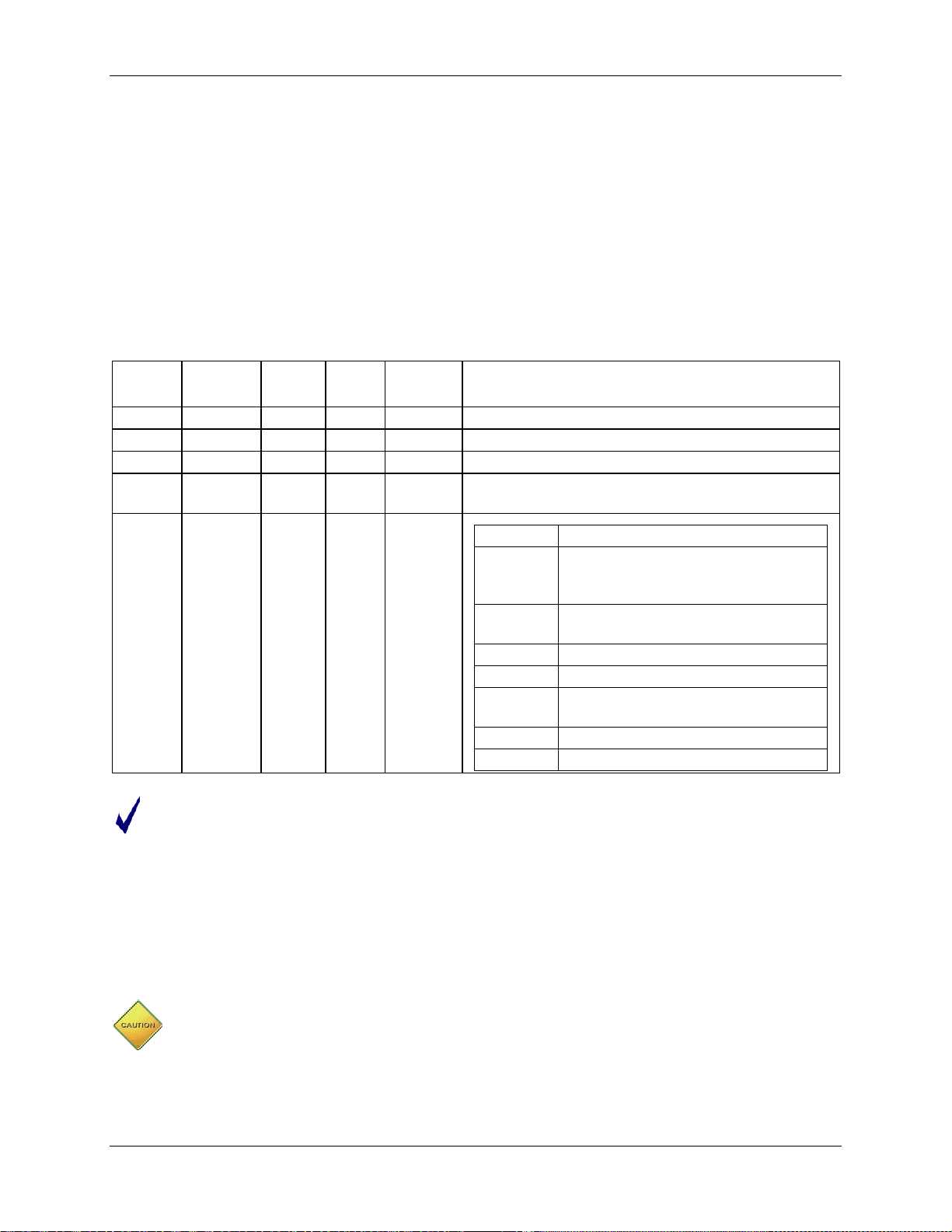
FDS 6531/6532 005 Data Sheet 71M6531D/F-71M6532D/F
Status
Read/
Reset
Two-Pin EEPROM Interface
The dedicated 2-pin serial interfac e commun icates wi th extern al EE PROM devices . The inter face is
multiplexed onto the DIO4 (SCK) and DI O 5 (SDA) pins and is selected by setting DIO_EEX[1:0] = 01.
The MPU communicates with the interface through the SFR registers EEDATA and EECTRL. If the MPU
wishes to write a byte of data to the EEPROM, it pl aces the data in EEDATA and then writes the Transmit
code to EECTRL. This initiates the transmit operation which is finished when the BUSY bit falls. INT5 is also
asserted when BUSY falls. The MPU can then check the RX_ACK bit to see if the EEPROM acknowledged
the transmission.
A byte is read by writing the Receive command to EECTRL and waiting for the BUSY bit to fall. Upon
completion, the received data is in EEDATA. The serial t rans m i t and receive clock is 78 kHz during each
transmission and then holds in a high state until the next transmission. The EECTRL bits when the two-pin
interface is selected are shown in Table 47.
Table 47: EECTRL Bits for 2-pin Interface
Bit
7
6
5
4
Name
ERROR
BUSY
RX_ACK
TX_ACK
Write
State
R 0 Positive 1 when an illegal command is received.
R 0 Positive 1 when serial data bus is busy.
R 1 Negative 0 indicates that the EEPROM sent an ACK bit.
R 1 Negative
Polarity Description
0 indicates when an ACK bit has been sent to the
EEPROM.
3:0
CMD[3:0]
W 0000 Positive
CMD[3:0] Operation
0000
No-op command. Stops the I2C
clock (SCK, DIO4). If not issued,
SCK keeps toggling.
0010
Receive a byte from the EEPROM
and send ACK.
0011 Transmit a byte to the EEPROM.
0101 Issue a STOP sequence.
0110
Receive the last byte from the
EEPROM and do not send ACK.
1001 Issue a START sequence.
Others No operation, set the ERROR bit.
The EEPROM interface can also be operated by controlling the DIO4 and DIO5 pins directly. In
this case, a resistor has to be used in series with S DA to avoid data collisions due to limits in the
speed at which the SDA pin can be switc hed from output to in put. Controlling DIO4 and DIO5
directly is discouraged, because it may tie up the MPU to the poi nt where it may become too busy
to process interrupts.
Three-Wire (µ-Wire) EEPROM Interface
A 500 kHz three-wire interface, using SDATA, SCK and a DIO pin for CS is available. The interface is
selected by setting DIO_EEX[1:0] = 2 (b10). The EECTRL bits when the three-wire interface is selected
are shown in Table 48. When EECTRL is written, up to 8 bits from EEDATA are either written to the
EEPROM or read from the EEPROM, depending on the values of the EECTRL bits.
The µ-Wire EEPROM interface is only funct i onal when MPU_DIV[2:0] = 000.
v1.3 © 2005-2010 TERIDIAN Semiconductor Corporation 47
Page 48
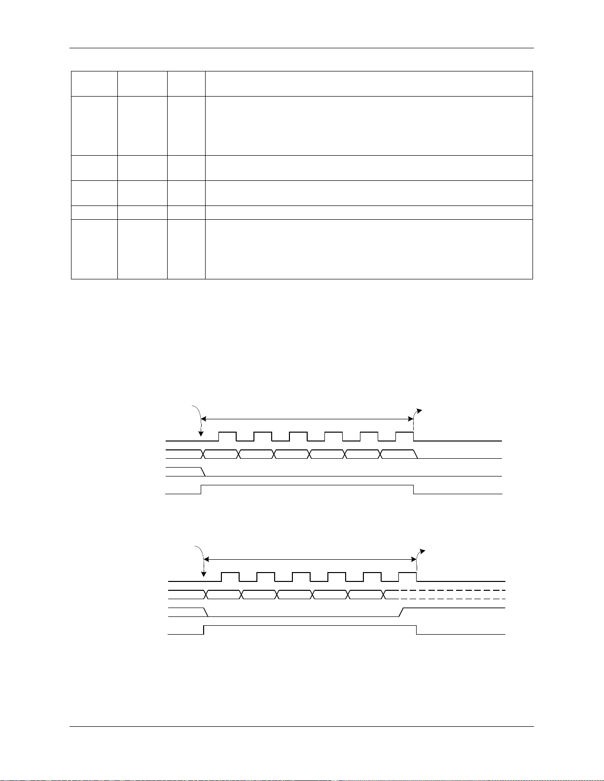
Data Sheet 71M6531D/F-71M6532D/F FDS 6531/6532 005
Bit
Write
SCLK (output)
BUSY (bit)
CNT Cycles (6 shown)
SDATA (output)
Write -- No HiZ
D2D3D4D5D6D7
EECTRL Byte Written
INT5
SDATA output Z
(LoZ)
CNT Cycles (6 shown)
Write -- Wi th HiZ
INT5
EECTRL Byte Written
SCLK (output)
BUSY (bit)
SDATA (output)
D2D3D4D5D6D7
(HiZ)(LoZ)
SDATA output Z
Table 48: EECTRL Bits for the 3-Wire Interface
Control
Name
Read/
Description
7
WFR
W
Wait for Ready. If this bit is set, the trailing edge of B US Y will be delayed
until a rising edge is seen on the data line. This bit can be used during
the last byte of a Write command to cause the I NT5 interrupt to occur
when the EEPROM has finished its internal write sequence. This bit is
ignored if HiZ = 0.
6
BUSY
R
Asserted while the serial data bus is busy. When the BUSY bit falls, an
INT5 interrupt occurs.
5
HiZ
W
Indicates that the SD signal is to be floated to high impedance immediately
after the last SCK rising edge.
4
3:0
RD
CNT[3:0]
W Indicates that EEDATA is to be filled with data from EEPROM.
W
Specifies the number of clocks to be issued. Allowed val ues are 0
through 8. If RD=1, CNT bits of data will be read MSB first and right
justified into the low order bits of EEDATA. If RD=0, CNT bits will be sent
MSB first to the EEPROM, shifted out of the MSB of EEDATA. If
CNT[3:0] is zero, SDATA will simply obey the HiZ bit.
The timing diagrams in Figure 11 through Figure 15 describe the 3-wire EEPROM interface behavior. All
commands begin when the EECTRL register is written. Transactions start by first raising the DIO pin that
is connected to CS. Multiple 8-bit or less commands such as t hose shown in Figure 11 through Figure 15
are then sent via EECTRL and EEDATA.
When the transaction is finished, CS must be l owered. At the end of a Read transaction, the EEPROM
will be driving SDATA, but will transition to HiZ (high impedance) when CS falls. The firmware should
then immediately issue a write command wit h CNT=0 and HiZ=0 to take control of SDATA and force it to
a low-Z state.
Figure 11: 3-Wire Interface. Write Command, HiZ=0
Figure 12: 3-Wire Interface. Write Command, HiZ=1
48 © 2005-2010 TERIDIAN Semiconductor Corporation v1.3
Page 49
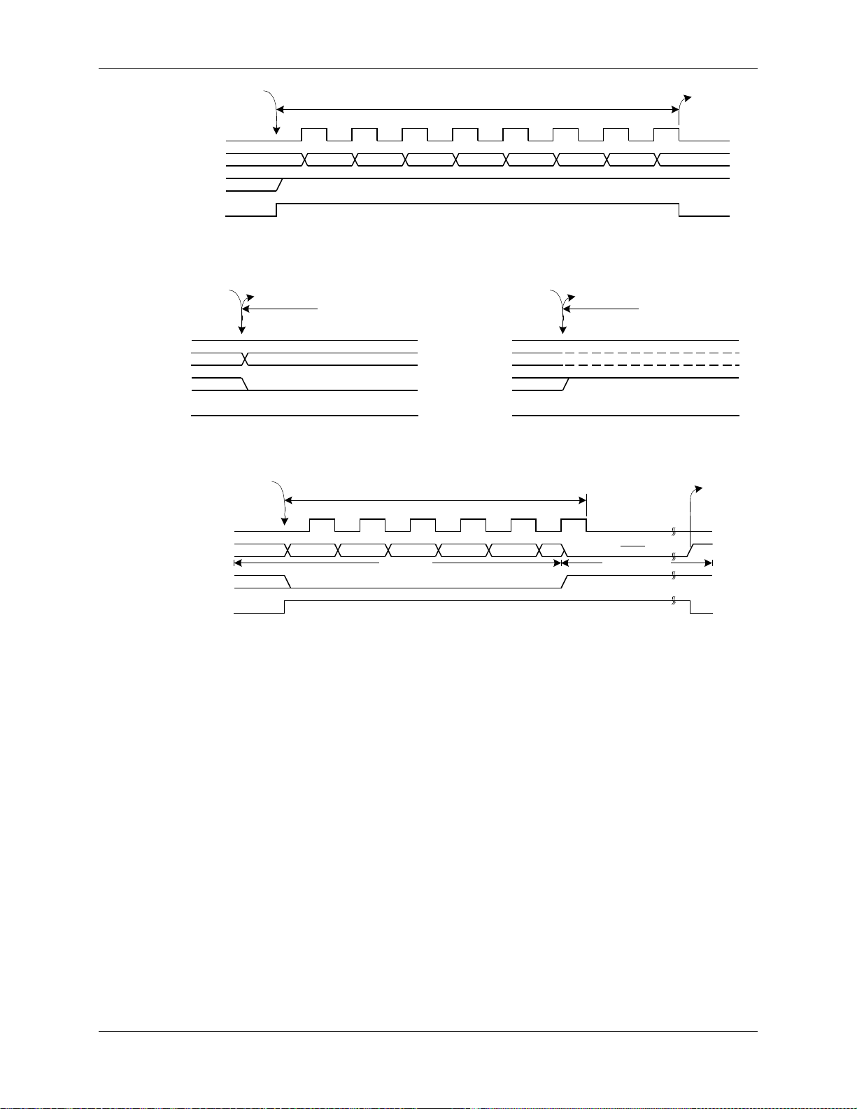
FDS 6531/6532 005 Data Sheet 71M6531D/F-71M6532D/F
CNT Cycles (8 shown)
READ
D0D1D2D3D4D5
INT5
D6D7
EECTRL Byte Written
SCLK (output)
BUSY (bit)
SDATA (input)
SDATA output Z
(HiZ)
CNT Cycles (0 shown)
Write -- No HiZ
D7
INT5 not issued
CNT Cycles (0 shown)
Write -- HiZ
INT5 not issued
EECTRL Byte Written EECTRL Byt e Written
SCLK (output)
BUSY (bit)
SDATA (output)
SCLK (output)
BUSY (bit)
SDATA (output)
(HiZ)
SDATA output ZSDATA output Z
(LoZ)
CNT Cycles (6 shown)
Write -- With HiZ and WFR
EECTRL Byte Written
SCLK (output)
BUSY (bit)
SDATA (out/in)
D2D3D4D5D6D7
BUSY
READY
(From EEPROM)
INT5
(From 6520)
SDATA output Z
(HiZ)(LoZ)
Figure 13: 3-Wire Interface. Read Command.
Figure 14: 3-Wire Interface. Write Command when CNT=0
Figure 15: 3-Wire Interface. Write Command when HiZ=1 and WFR=1
1.5.15 SPI Slave Port
The slave SPI port communicates directl y with the MPU data bus and is able to read and write Data RAM
locations. It is also able to send commands to the MPU. The interface to the slave port consists of the
PCSZ, PCLK, PSDI and PSDO pins. These pins are multiplexed with the LCD segment driver pins SEG3
to SEG6. The port pins default to LCD driver pins. The port is enab l ed by setting the SPE bit.
A typical SPI transaction is as follows. While PCSZ is high, the port is held in an initialized/reset state.
During this state, PSDO is held in HiZ state and all tra nsitions on PCLK and PSDI are ignored. When
PCSZ falls, the port will begin the transaction on the first rising edge of PCLK. A transaction consists of
an 8-bit command, a 16-bit address and then one or more bytes of data. The transaction ends when
PCSZ is raised. Some transactions may consist of a command only.
The last SPI command and address (if part of the co m m and) are available to the MPU in registers
SP_CMD and SP_ADDR.
The SPI port supports data transfers at 1 Mb/s in mission mode and 16 kb/s in brownout mode. The SPI
commands are described in Table 49 and in Figure 16 illustrate the SPI Interface read and write timing.
v1.3 © 2005-2010 TERIDIAN Semiconductor Corporation 49
Page 50
Data Sheet 71M6531D/F-71M6532D/F FDS 6531/6532 005
Command
Description
Table 49: SPI Command Description
11xx xxxx ADDR Byte0 ... ByteN Read data starting at ADDR. The ADDR will auto-increment until PCSZ
is raised. Upon completion:
SP__CMD=11xx xxxx, SP_ADDR=ADDR+N+1.
No MPU interrupt is generated if the command is 1100 0000. Otherwise,
an SPI interrupt is generated.
10xx xxxx ADDR Byte0 ... ByteN Write data starting at ADDR. The ADDR will auto-increment until PCSZ
is raised. Upon completion:
SP_CMD=10xx xxxx, SP_ADDR=ADDR+N+1.
No MPU interrupt is generated if the command is 1000 0000. Otherwise,
an SPI interrupt is generated.
Certain I/O RAM registers can be written and read using the SPI port (see Table 50). However, the MPU
takes priority over the I/O RAM bus, and SP I operation may fail without notice. To avoid this situation, the
SPI host should send a command other than 11x xxxxx or 10xxxxxx (read or write) before the act ual read
or write command. The SPI slave interface will load the command register and generate an INT2 interrupt upon receiving the command. The MPU should service the interrupt and halt any external data memory
operations to effectively grant the bus to the SPI. When the SPI host finishes, it should send another
command so the MPU can release the bus. There ar e no i ssues with Data RAM access; SPI and the
MPU will share the bus with no conflicts for Data RA M access.
Table 50: I/O RAM Registers Accessible via SPI
Name Address (hex) Bit Range Read/Write
CE0 2000 7:3 RW
CE1 2001 7:0 RW
CE2 2002 5:3, 1:0 RW
CONFIG0 2004 7:6, 3:0 RW
CONFIG1 2005 5:2, 0 RW
VERSION 2006 7:0 R
CONFIG2 2007 7:0 RW
DIO0 2008 7:6, 4:0 RW
DIO1 to DIO6 2009 to 200E 6:4, 2:0 RW
− 200F 7:6, 3:2 RW
RTM0H 2060 1:0 RW
RTM0L 2061 7:0 RW
RTM1H 2062 1:0 RW
RTM1L 2063 7:0 RW
RTM2H 2064 1:0 RW
RTM2L 2065 7:0 RW
RTM3H 2066 1:0 RW
RTM3L 2067 7:0 RW
PLS_W 2080 7:0 RW
PLS_I 2081 7:0 RW
SLOT0 to SLOT9 2090 to 209A 7:0 RW
CE3 209D 3:0 RW
CE4 20A7 7:0 RW
CE5 20A8 7:0 RW
WAKE 20A9 7:5, 3:0 R
CONFIG3 20AC 5:4, 1:0 RW
CONFIG4 20AD 5:4, 1:0 RW
− 20AF 2:0 RW
50 © 2005-2010 TERIDIAN Semiconductor Corporation v1.3
Page 51
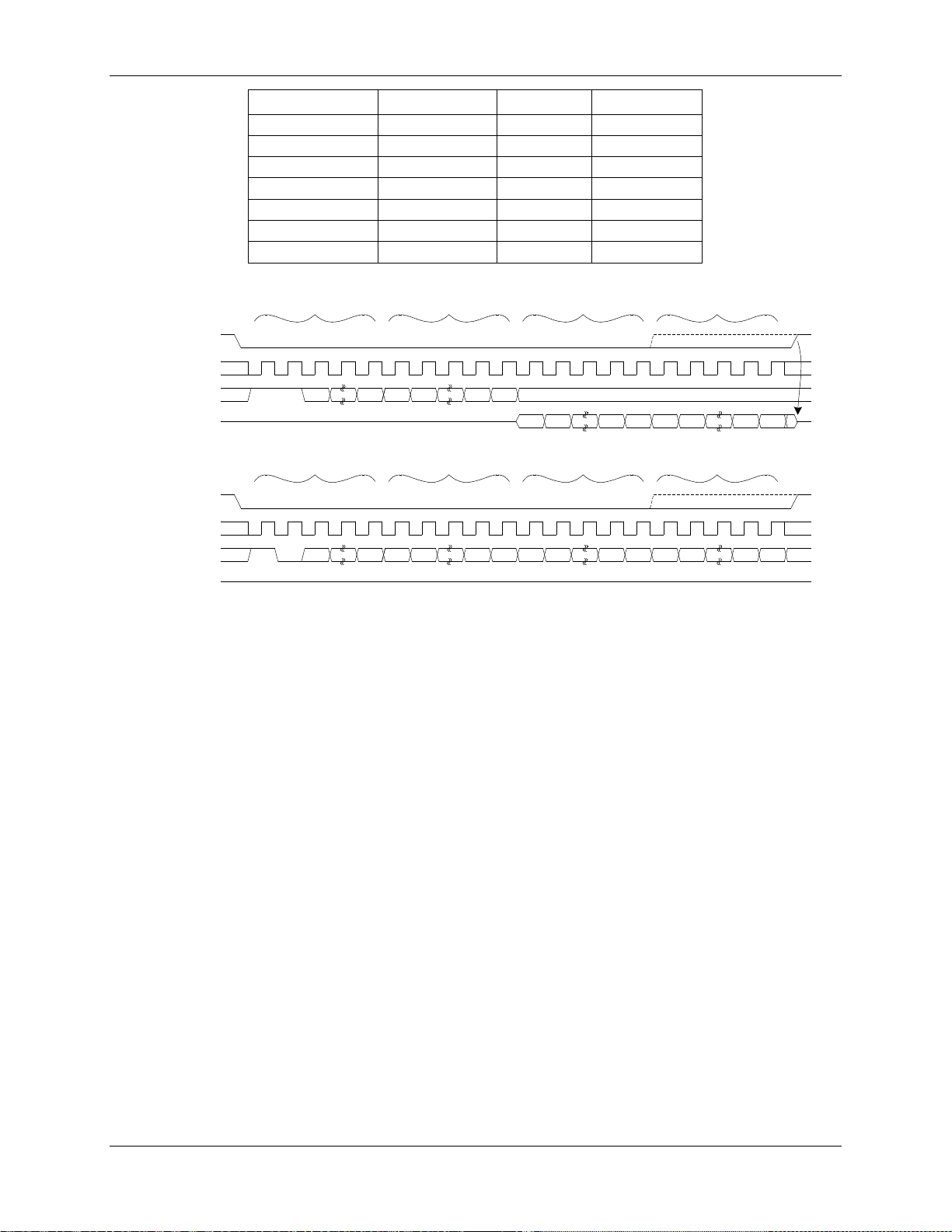
FDS 6531/6532 005 Data Sheet 71M6531D/F-71M6532D/F
VERSION
20C8
7:0
R
TRIMX
20FE
0
RW
A15 A14
A1 A0C0
0 31
x
D7 D6 D1 D0 D7 D6 D1 D0
C5C6C7
x
PCSZ
PSCK
PSDI
PSDO
8 bit CMD 16 bit Address
DATA[ADDR]
DATA[ADDR+1]
7 8 23 24 32 39
Extended Read . . .
SERIAL READ
A15 A14
A1 A0C0
0 31
C5C6C7
x
PCSZ
PSCK
PSDI
PSDO
8 bit CMD 16 bit Address
DATA[ADDR]
DATA[ADDR+1]
7 8 23 24 32 39
Extended Write . . .
SERIAL WRITE
D7 D6
D1 D0 D7
D6 D1 D0
x
HI Z
HI Z
(From Host)
(From 6531)
(From Host)
(From 6531)
Name Address (hex) Bit Range Read/Write
SPI0 20B0 4, 0 RW
SPI1 20B1 4, 0 R
CHIP_ID 20C9 7:0 R
TRIMSEL 20FD 4:0 RW
TRIM 20FF 7:0 RW
Figure 16: SPI Slave Port: Typical Read and Write operations
Possible applications for the SPI interface are:
1) An external host reads data from CE locations to obtain metering information. This c an be used in
applications where the 71M6531D/F or 71M6532D/F function as smart front-ends with preprocessing
capability. Since the addresses are in 16-bit format , any type of XRAM data can be accessed: CE ,
MPU, I/O RAM, but not SFRs or the 80515-internal register bank.
2) A communication link can be established via the SPI interface: By writing into MPU memory locations,
the external host can initiate and control proce ss es in the MPU of the 71M6531D/F or 71M6532D/F.
Writing to a CE or MPU location normally generat es an interrupt, a function that can be used to signal
to the MPU that the byte that had just been written by the external host must be read and processed.
Data can also be inserted by the external host without generating an interrupt.
3) An external DSP can access front-end data generated by the ADC. This mode of operation u ses the
71M6531D/F or 71M6532D/F as an analog front-end (AF E ).
v1.3 © 2005-2010 TERIDIAN Semiconductor Corporation 51
Page 52
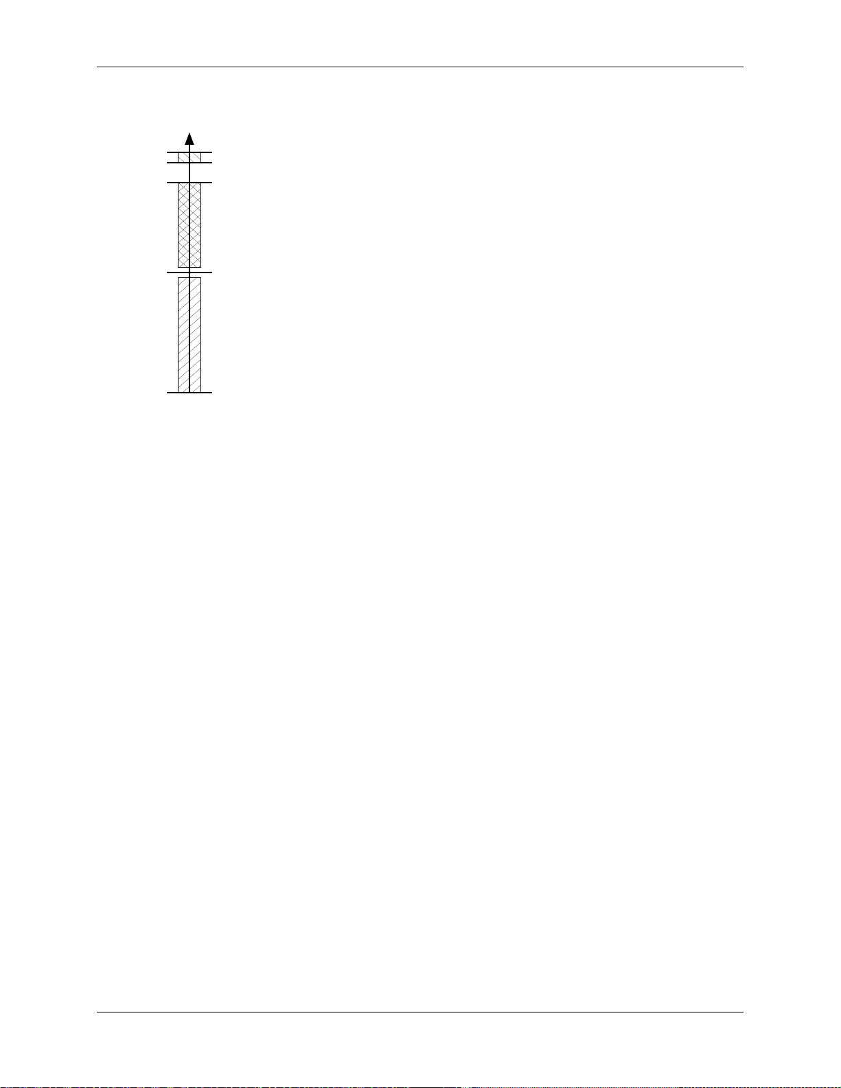
Data Sheet 71M6531D/F-71M6532D/F FDS 6531/6532 005
V3P3
V3P3 -
400mV
V3P3 - 10mV
VBIAS
0V
Battery
modes
Normal
operation,
WDT
enabled
WDT dis-
abled
V1
1.5.16 Hardware Watchdog Timer
An independent, robust, fixed-duration, watchdog timer (WDT) is i ncluded
in the 71M6531D/F and 71M6532D/F. It uses the RTC cry st al oscillator as
its time base and must be refreshed by the MPU firmwar e at least every
1.5 seconds. When not refreshed on time, the WDT overflows and the part
is reset as if the RESET pin were pulled high, except that the I/O RAM bits
will be in the same state as after a wake-up from SLEEP or LCD modes
(see the I/O RAM description in Section 4.2 for a list of I/O RAM bit states
after RESET and wake-up). 4100 oscillator cycles (or 125 ms) aft er the
WDT overflow, the MPU will be launched from program address 0x0000.
A status bit, WD_OVF, is set when the WDT overflow occurs. This bit is
powered by the nonvolatile supply and can be read by the MPU when
WAKE rises to determine if the part is initializing after a WDT overflow
event or after a power-up. After it is read, the MPU firmware must clear
WD_OVF. The WD_OVF bit is also cleared by the RESET pin.
There is no internal digital state that deactiv ates the WDT.
Figure 17: Functions defined by V1
The WDT can be disabled by tying the V1 pin to V3P3 (see Figure 17). Of course, this also deactivates
V1 power fault detection. Since there is no method in firmware to disable the crystal oscillator or the
WDT, it is guaranteed that whatever state the part might find itself in, upon watchdog overflow, the part
will be reset to a known state.
Asserting ICE_E will also deactivate the WDT. This is the only method that will work in BROWNOUT
mode. In normal operation, the WDT is reset by periodically writing a one to the WDT_RST bit. The
watchdog timer is also reset when the internal signal WAKE = 0 (see Section 2.5 Wake-Up Behavior).
If enabled with the IEN_WD_NROVF bit in I/O RAM, an interrupt occurs roughly 1 ms before the WDT resets
the chip. This can be used to determine the cause of a WDT reset since it allows the code to log i ts state
(e.g. the current PC value, loop counters, flags, etc.) before a WDT reset occurs.
52 © 2005-2010 TERIDIAN Semiconductor Corporation v1.3
Page 53

FDS 6531/6532 005 Data Sheet 71M6531D/F-71M6532D/F
1.5.17 Test Ports (TMUXOUT pin)
One of the digital or analog signals listed i n Table 51 can be selected to be output on the TMUXOUT pin.
The function of the multiplexer is controlled with the I/O RAM field TMUX[4:0] (0x20AA[4:0]), as shown in
Table 51.
Table 51: TMUX[4:0] Selections
TMUX[4:0] Mode Function
0 Analog GNDD
1 Analog Reserved
2 Analog GNDD
3 Analog Reserved
4 Analog PLL_2P5
5 Analog Output of the 2.5 V low-power regulator
6 Analog Internal VBIAS voltage (nominally 1.6V)
7 Analog Not used
8 - 0x0F – Reserved
0x10 Digital RTC 1-second output
0x11 Digital RTC 4-second output
0x12 – Not used
0x13 Digital V1_OK comparator output
0x14 Digital Real-time output (RTM) from the CE
0x15 Digital WDTR_EN (Comparator 1 Output AND V1LT3)
0x16 – 0x17 – Not used
0x18 Digital RXD (from Optical interface, w/ optional inversion)
0x19 Digital MUX_SYNC
0x1A – Not used
0x1B Digital CKMPU (MPU clock)
0x1C Digital Pulse output
0X1D Digital
0X1E Digital CE_BUSY (busy interrupt generated by CE, 396µs)
0X1F Digital
RTCLK (output of the oscillator circuit, nominally
32,786Hz)
XFER_BUSY (transfer busy interrupt generated by the
CE, nominally every 999.7ms)
The TMUXOUT pin may be used for diagnosis purposes or in production test. The RTC 1-second output
may be used to calibrate the crystal oscillator. The RTC 4-second output provides even higher precision.
v1.3 © 2005-2010 TERIDIAN Semiconductor Corporation 53
Page 54
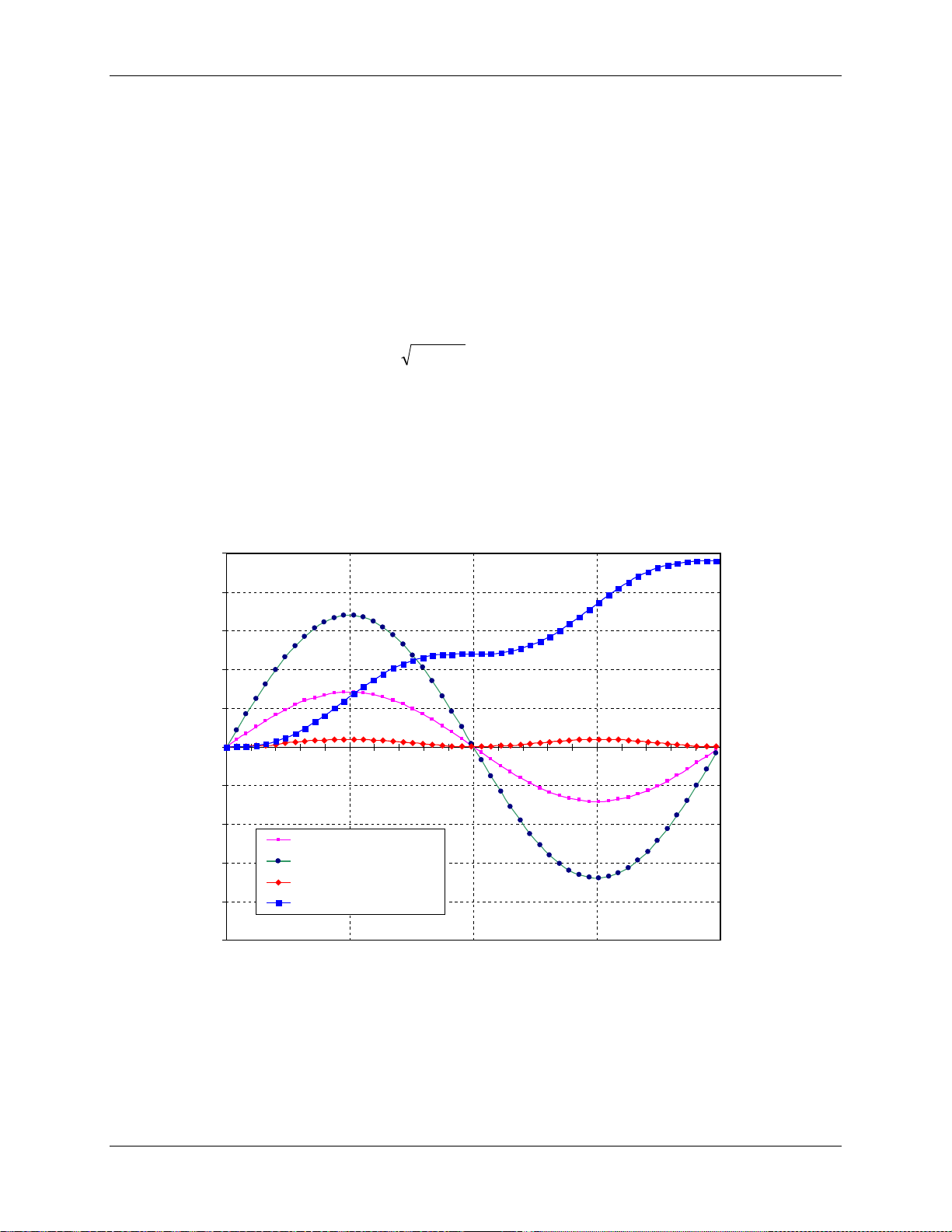
Data Sheet 71M6531D/F-71M6532D/F FDS 6531/6532 005
∫
=
t
dttItVE
0
)()(
22
QP +
-500
-400
-300
-200
-100
0
100
200
300
400
500
0 5 10 15 20
Current [A]
Voltage [V]
Energy per Interval [Ws]
Accumulated Energy [Ws]
2 Functional Description
2.1 Theory of Operation
The energy delivered by a power source int o a l oad can be expressed as:
Assuming phase angles are constant, the following formulae apply:
P = Real Energy [Wh] = V * A * cos φ* t
Q = Reactive Energy [VARh] = V * A * sin φ * t
S = Apparent Energy [VAh] =
For a practical meter, not only voltage and current amplitudes, but also phase angles and harmonic content
may change constantly. Thus, simple RMS measurements are inherently inaccurate. A modern solid-state
electricity meter IC such as the Teridian 71M6531 functions by emulating the integral operation above, i.e.
it processes current and voltage samples through an ADC at a constant frequency. As long as the ADC
resolution is high enough and the sample frequency is beyon d the harmonic range of interest, the current
and voltage samples, multiplied with the ti m e peri od of sampling will yield an accurate quantity for the
momentary energy. Summing up the momentary energy quantities over time will result in accumulated
energy.
Figure 18 shows the shapes of V(t), I(t), the mom entary power and the accumulated power, resulting from
50 samples of the voltage and current signals over a period of 20 ms. The application of 240 VAC and 100 A
results in an accumulation of 480 Ws (= 0.133 Wh) over the 20 ms period, as indicated by the accumulated
power curve. The described sampling method works reliably, even in the presence of dynamic phase shift
and harmonic distortion.
54 © 2005-2010 TERIDIAN Semiconductor Corporation v1.3
Figure 18: Voltage, Current, Momentary and Accumulated Energy
Page 55
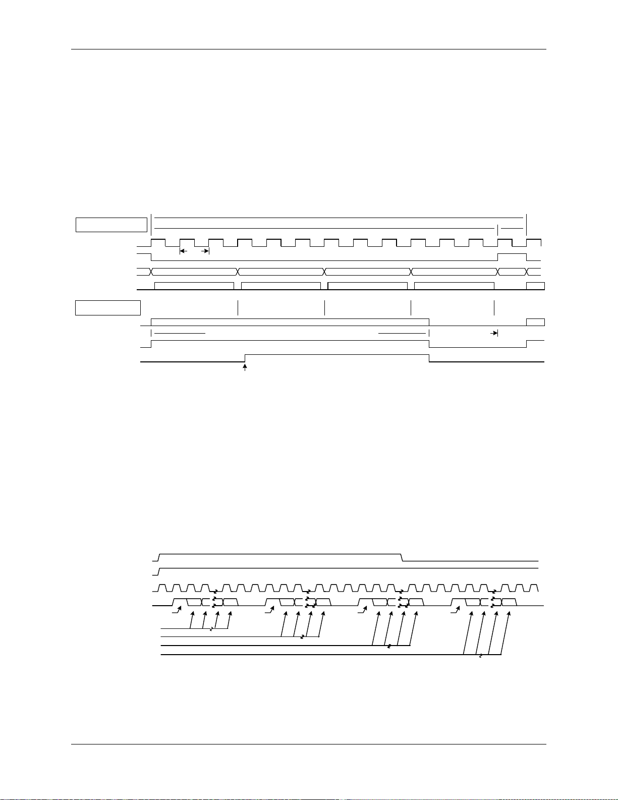
FDS 6531/6532 005 Data Sheet 71M6531D/F-71M6532D/F
FLAG
RTM DATA 0 (32 bits)
0 1 0 1
0 1 0 1
FLAG
FLAG
FLAG
CK32
MUX_SYNC
CKTEST
TMUXOUT/RTM
LSB
LSB
SIGN
SIGN
LSB
SIGN
30 31 30 31
30
31
30 31
LSB
SIGN
RTM DATA 1 (32 bits)
RTM DATA 2 (32 bits)
RTM DATA 3 (32 bits)
CK32
MUX STATE
0
MUX_DIV=4 (4 conversions) is shown
Settle
ADC MUX Frame
ADC EXECUTION
S
MUX_SYNC
S
CE_EXECUTION
MAX CK COUNT
0 450
150
900 1350 1800
ADC0 ADC1 ADC2 ADC3
CK COUNT = CE_CYCLES + floor((CE_CYCLES + 2) / 5)
NOTES:
1. ALL DIMENSIONS ARE 5MHZ CK COUNTS.
2. THE PRECISE FREQUENCY OF CK IS 150*CRYSTAL FREQUENCY = 4.9152MHz.
3. XFER_BUSY OCCURS ONCE EVERY (PRE_SAMPS * SUM_CYCLES) CODE PASSES.
CE_BUSY
XFER_BUSY
INITIATED BY A CE OPCODE AT END OF SUMMATION INTERVAL
ADC TIMING
CE TIMING
1 2 3
2.2 System Timing Summary
Figure 19 summarizes the timing relatio nships between the input MUX states, the CE_BUSY signal and
the two serial output streams. In this example, MUX_DIV[3:0] = 4 and FIR_LEN[1:0] = 2 (384 CE cycles,
3 CK32 cycles per conversion), resulting i n 13 CK32 cycles per multiplexer frame. Generally, the duration
of each MUX frame is:
• 1 + MUX_DIV * 1, if FIR_LEN[1:0] = 0 (138 CE cycles)
• 1 + MUX_DIV * 2, if FIR_LEN[1:0] = 1 (288 CE cycles)
• 1 + MUX_DIV * 3, if FIR_LEN[1:0] = 2 (384 CE cycles).
An ADC conversion will always consume an intege r number of CK32 clocks. Following this is a single
CK32 cycle where the bandgap voltage is allowed to recover from the change in CROSS.
Figure 19: Timing Relationship between ADC MUX, Compute Engine
Each CE program pass begins when the ADC0 conversion (for IA) begins. Depending on the length of
the CE program, it may continue running until the end of the last conversion (ADC3). CE opcodes are
constructed to ensure that all CE code passes consume exactly the same number of cycles. The result of
each ADC conversion is inserted into the RAM when the conversion is complete. The CE code is written
to tolerate sudden changes in ADC data. The exact clock count when each ADC value is loaded into
RAM is shown in Figure 19.
Figure 20 shows that the serial data stream, RTM , begins transmitting at the beginning of state S. RTM,
consisting of 140 CK cycles, will always finish bef ore the next code pass starts.
Figure 20: RTM Output Format
v1.3 © 2005-2010 TERIDIAN Semiconductor Corporation 55
Page 56
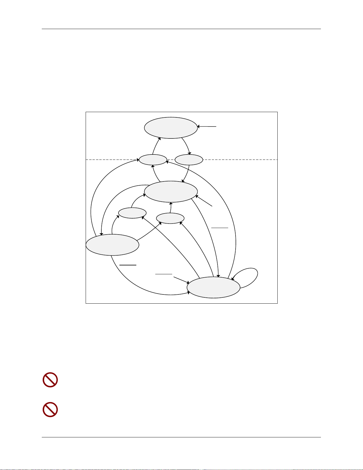
Data Sheet 71M6531D/F-71M6532D/F FDS 6531/6532 005
V3P3SYS
rises
V3P3SYS
falls
MISSION
BROWNOUT
LCD
SLEEP or
V1 > VBIAS
V1 <= VBIAS
LCD_ONLY
RESET &
VBAT_OK
RESET
IE_PLLRISE IE_PLLFALL
IE_PB
IE_WAKE
PB
timer
timer
PB
RESET &
V3P3SYS
rises
V3P3SYS
rises
VBAT_OK
VBAT_OK
VBAT_OK
VBAT_OK
SLEEP
2.3 Battery Modes
Shortly after system power (V3P3SYS) is appli ed, the part will be in MISSION mode. MISSION mode
means that the part is operating with system power and that the internal PLL is stable. This mode is the
normal operation mode where the part is capa bl e of measuring energy.
When system power is not available (i.e. when V 1<VBIAS), the 71M6531 will be in one of three battery
modes: BROWNOUT, LCD, or SLEEP mode. Figure 21 shows a state diagram of the various operation
modes, with the possible transitions between m odes. For information on the timing of mode transitions
refer to Figure 22 through Figure 24.
When V1 falls below VBIAS or the part wakes up un der battery power, the part will automatically enter
BROWNOUT mode (see Section 2.5 Wake-Up Behavior). From BROWNO UT mode, the part may enter
either LCD mode or SLEEP mode, as controlled by the MPU via the I/O RAM bits LCD_ONLY and SLEEP.
Figure 21: Operation Modes State Diagram
The transition from MISSION mode to BROWNOUT mode is signaled by the IE_PLLFALL interrupt flag
(SFR 0xE8[7]). The transition in the other direction is signaled by the IE_PLLRISE interrupt flag (SFR
0xE8[6]), when the PLL becomes stable.
Meters that do not require functionality in the battery modes, e.g. meters that only use the SLE E P
mode to maintain the RTC, still need to contain c ode that brings the chip from BROWNOUT
mode to SLEEP mode. Otherwise, the chip remains in BROWNOUT mode once the system
power is missing and consumes more current than intended.
Similarly, meters equipped with batteries need to contain code that transitions the chip to SLEEP
mode as soon as the battery is attached in producti on. Otherwise, remaining in BROWNOUT
mode would unnecessarily drain the battery.
56 © 2005-2010 TERIDIAN Semiconductor Corporation v1.3
Page 57
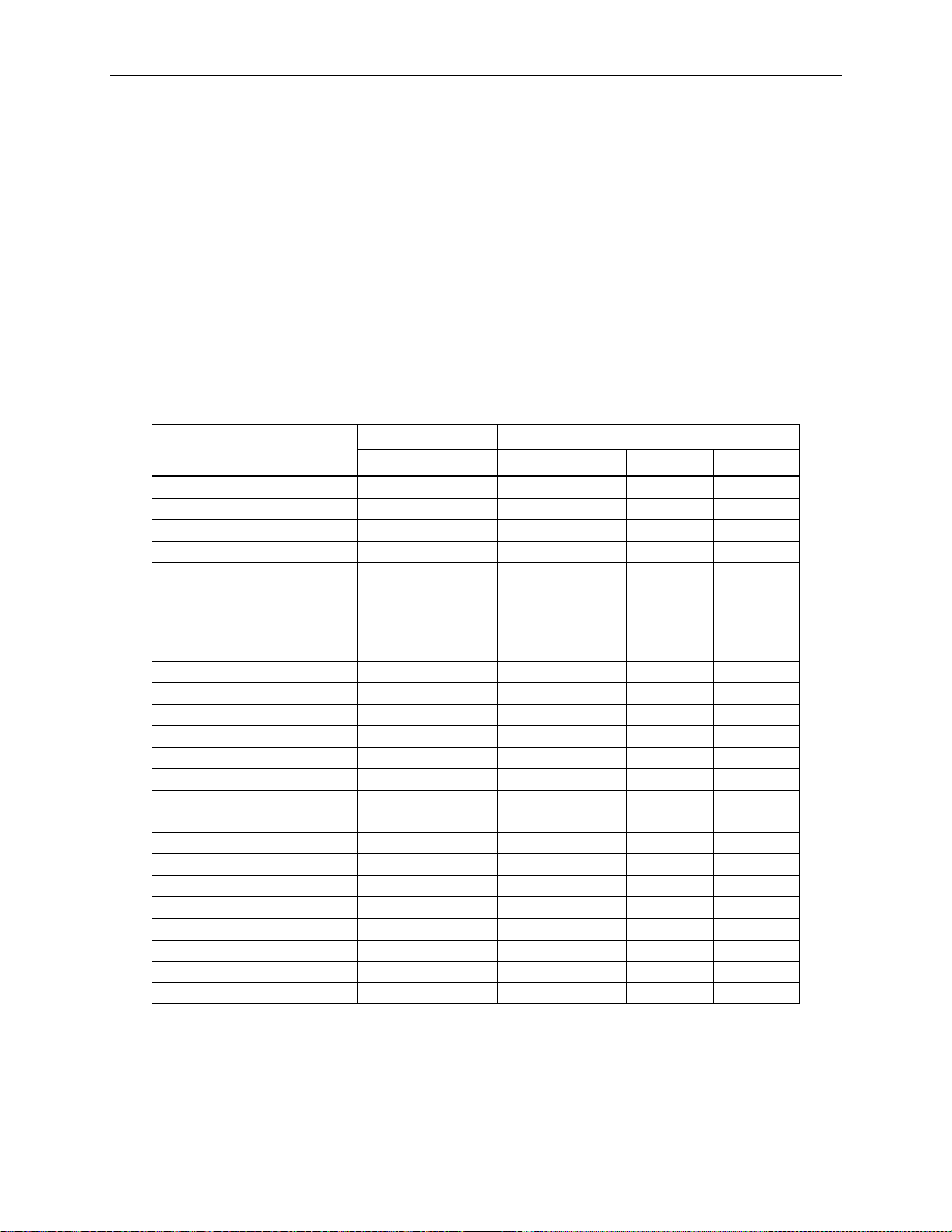
FDS 6531/6532 005 Data Sheet 71M6531D/F-71M6532D/F
CE
Yes
–
–
–
OSC and RTC
Yes
Yes
Yes
Yes
To facilitate transition to sleep mode, which is useful when an unprogrammed IC is mount ed on a PCB
with a battery installed, the Teridian production test programs the following six-byte sequence int o the
flash location starting at address 0x00000: 0x 74 - 0x40 - 0x90 - 0x20 - 0xA9 - 0xF0. This sequence decodes to the following assembler code:
0000: 7440 MOV A,#40 ; set bit 6 in accumulator
0002: 9020A9 MOV DPTR,#20A9 ; point to I/O RAM address 0x20A9
0005: F0 MOVX @DPTR,A ; set bit 6 (sleep) in 0x20A9
Transitions from both LCD and SLEEP mode are ini tiated by the wake-up timer timeout conditions or
pushbutton events. When the PB pin is pulled high (pushbutt on i s pressed), the IE_PB interrupt flag (SFR
0xE8[4]) is set, and when the wake-up timer times out, the IE_WAKE interrupt flag (SFR 0xE8[ 5]) is set.
In the absence of system power, if the voltage margin for the LDO regulator providing 2.5 V to the internal
circuitry becomes too low to be safe, the part automatically enters sleep mode (BAT_OK false). The battery
voltage must stay above 3 V to ensure that BA T _OK remains true. Under this condition, the 71M6531
stays in SLEEP mode, even if the voltage margin for the LDO improves (BAT_ O K true). Table 52 shows
the circuit functions available in each operating mode.
Table 52: Available Circuit Functions
Circuit Function
CE Data RAM Yes Yes – –
FIR Yes – – –
Analog circuits Yes – – –
MPU clock rate
MPU_DIV[2:0]
ICE Yes Yes – –
DIO Pins Yes Yes – –
Watchdog Timer Yes Yes – –
LCD Yes Yes Yes –
EEPROM Interface (2-wire) Yes Yes (8 kb/s) – –
EEPROM Interface (3-wire) Yes Yes (16 kb/s) – –
UART Yes 300 bd – –
Optical TX modulation Yes – – –
Flash Read Yes Yes – –
Flash Page Erase Yes Yes – –
Flash Write Yes – – –
RAM Read and Write Yes Yes – –
Wakeup Timer Yes Yes Yes Yes
System Power Battery Power (Nonvolatile Supply)
MISSION BROWNOUT LCD SLEEP
From PLL, as
defined by
MPU_DIV[2:0]
Yes – – –
28.672 kHz
(7/8 of 32768 Hz)
– –
XRAM data preservation Yes Yes – –
V3P3D voltage output pin Yes Yes – –
GPO – GP7 registers Yes Yes Yes Yes
– indicates not active
2.3.1 BROWNOUT Mode
In BROWNOUT mode, most non-metering digital functions are active (as shown in Table 52), including
ICE, UART, EEPROM, LCD and RTC. In BROWNOUT mode, a low bias current regulator will provide
2.5 Volts to V2P5 and V2P5NV. The regulator has an output called BAT_OK to indicate that it has sufficient
overhead. When BAT_OK = 0, the part will enter SLE EP mode. From BROWNOUT mode, the processor
v1.3 © 2005-2010 TERIDIAN Semiconductor Corporation 57
Page 58

Data Sheet 71M6531D/F-71M6532D/F FDS 6531/6532 005
can voluntarily enter LCD or SLEEP modes. When system power is restored, the part will automatically
transition from any of the battery modes to MISSION mode, once the PLL has settled.
The MPU will run at 7/8 of the crystal clock rat e. Thi s permits the UARTs to be operated at 300 bd. In
this mode, the MPU clock has substantial short-term jitter.
The value of MPU_DIV[2:0] will be remembered (not changed) as the part enters and exits BROWNOUT.
MPU_DIV[2:0] will be ignored during BROWNOUT.
While PLL_OK = 0, the I/O RAM bits ADC_E and CE_E are held in the zero state disabling both the ADC and
the CE. When PLL_OK falls, the CE program counter is cleared immediately and all FIR processing halts.
2.3.2 LCD Mode
In LCD mode, the data contained in the LCD_SEGn[3:0] fields is displayed. Up to four LCD segm ents,
each connected to pins SEG18 and SEG19, can be made to blink without the involvement of the MPU,
which is disabled in LCD mode. To minimize power , only segments that might be used should be
enabled.
LCD mode can be exited only by system power up, a timeout of the wake-up ti m er, or a push button.
When the IC exits LCD mode, the MPU can discover the event that caused the exit by reading the interrupt
flags and interpret them as follows:
• IE_WAKE = 1 indicates that the wake timer has expir ed.
• IE_PB =1 indicates that the pushbutton input (P B ) was activated.
• COMPSTAT = 0 indicates that a reset occurred but that main power is not yet available.
• If none of the above conditions applies, syst em power (V3P3SYS) must have been restored
After the transition from LCD mode to MISSION or BROWNOUT mode, the PC will be at 0x0000, the
XRAM is in an undefined state and the I/O RAM is only partially preserved (see the description of I/O RAM
states in Section 4.2). The GP0[7:0] through GP7[7:0] registers are preserved unless RESET goes high.
2.3.3 SLEEP Mode
In SLEEP mode, the battery current is mini m i zed and only the Oscillator and RTC functions a re act ive.
This mode can be exited only by system power-up, a timeout of the wake-up timer, or a push button event.
When the IC exits SLEEP mode, the MPU can discover the e vent tha t caused the exit by read ing the
interrupt flags and interpret them as follows:
• IE_WAKE = 1 indicates that the wake timer has expir ed.
• IE_PB =1 indicates that the pushbutton input (P B) was activated.
• COMPSTAT = 0 indicates that a reset occurred but that main power is not yet available.
• If none of the above conditions applies, syst em power (V3P3SYS) must have been restored
After the transition from SLEEP mode to MISSION or BROWNOUT mode the PC will be at 0x0000, the
XRAM is in an undefined state and the I/O RAM is only partially preserved (see the description of I/O RAM
states in Section 4.2). The GP0[7:0] through GP7[7:0] registers are preserved unless RESET goes high.
58 © 2005-2010 TERIDIAN Semiconductor Corporation v1.3
Page 59
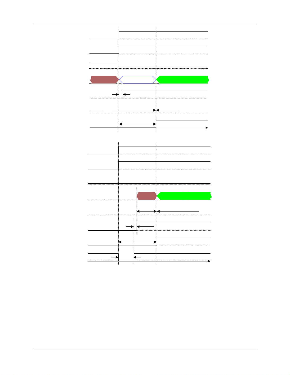
FDS 6531/6532 005 Data Sheet 71M6531D/F-71M6532D/F
time
System
Power
(V3P3SYS)
MPU Mode
Battery
Current
Transition
MPU Clock
Source
Xtal
PLL
(4.2MHz/MUX_DIV)
PLL_OK
MISSION
2048...4096
CK32 cycles
300nA
13..14 CK
cycles
WAKE
BROWNOUT
V1_OK
time
V3P3SYS
and VBAT
MPU Mode
Battery
Current
MPU Clock
Source
Xtal
PLL
(4.2MHz)
PLL_OK
MISSION
300nA
WAKE
Internal
RESETZ
BROWN-
OUT
1024 CK32
cycles
14.5 CK32
cycles
4096 CK32
cycles
V1_OK
Figure 22: Transition from BROWNOUT to MISSION Mode when System Power Returns
Figure 23: Power-Up Timing with V3P3SYS and VBAT tied together
v1.3 © 2005-2010 TERIDIAN Semiconductor Corporation 59
Page 60
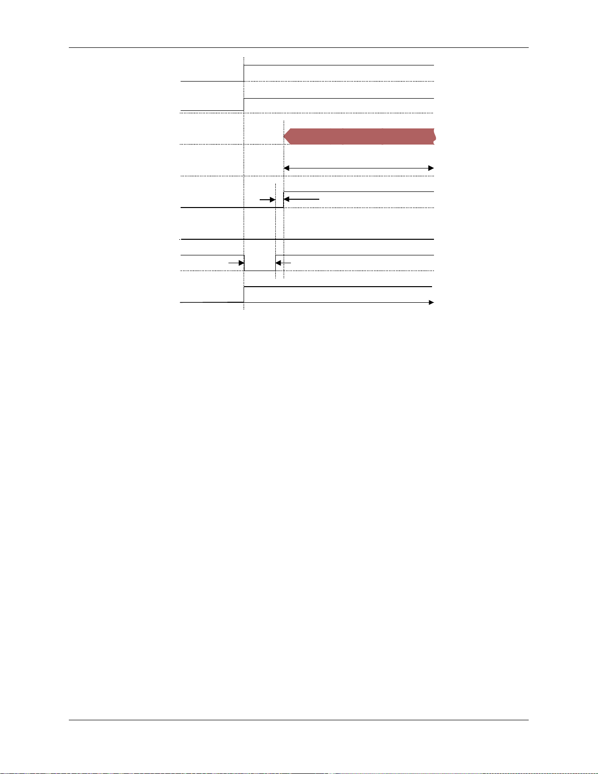
Data Sheet 71M6531D/F-71M6532D/F FDS 6531/6532 005
time
VBAT
MPU Mode
Battery
Current
MPU Clock
Source
Xtal
PLL_OK
WAKE
Internal
RESETZ
1024 CK32
cycles
BROWNOUT
14.5 CK32
cycles
VBAT_OK
Figure 24: Power-Up Timing with VBAT only
2.4 Fault and Reset Behavior
2.4.1 Reset Mode
When the RESET pin is pulled high, all digital act ivity stops. The oscillator and RTC module continue to
run. Additionally, all I/O RAM bits are set to thei r default states. As long as V1, the input voltage at the
power fault block, is greater than VBIAS , the internal 2.5 V regulator will continue to provide power to the
digital section.
Once initiated, the reset mode will persist unt i l the reset timer times out, signified by WAKE rising. This
will occur in 4100 cycles of the real time clock af ter RESET goes low, at which time the MPU will begi n
executing it’s pre-boot and boot sequences from address 00. See the Program Security description in the
Flash Memory section for additional descriptions of pre-boot and boot.
If system power is not present, the reset t i m er duration will be 2 cycles of the crystal clock at which time
the MPU will begin executing in BROWNOUT m ode, starting at address 00.
2.4.2 Power Fault Circuit
The 71M6531D/F and 71M6532D/F include a comparator to monitor system power fault conditions.
When the output of the comparator falls (V1<VBIAS), the I/O RAM bits PLL_OK are zeroed and the part
switches to BROWNOUT mode if a battery is present. Once system power returns, the MPU remains in
reset and does not transition to MISSION mode until 2048 to 4096 CK32 clock cycles later, when PLL_OK
rises. If a battery is not present, as indicated by BAT_OK=0, WAKE will fall and the part will enter SLEEP
mode.
There are several conditions the device could be in as system power returns. If the part is in BROWNOUT
mode, it will automatically switch to MISSION mode when PLL_OK rises. It will receive an interrupt indicating
this. No configuration bits will be reset or reconfigured durin g this transition.
If the part is in LCD or SLEEP mode when system power returns, it will also switch to MISSION mode
when PLL_OK rises. In this case, all configuration bi ts will be in the reset state due to WAKE having
been zero. The RTC clock will not be disturbed, but t he M PU RAM must be re-initialized. The hardware
watchdog timer will become active when the part enters MISSION mode.
If there is no battery when system power returns, the part will switch to MISSION mode when PLL_OK
rises. All configuration bits will be in reset state and RTC and MPU RAM data will be unknown and must
be initialized by the MPU.
60 © 2005-2010 TERIDIAN Semiconductor Corporation v1.3
Page 61
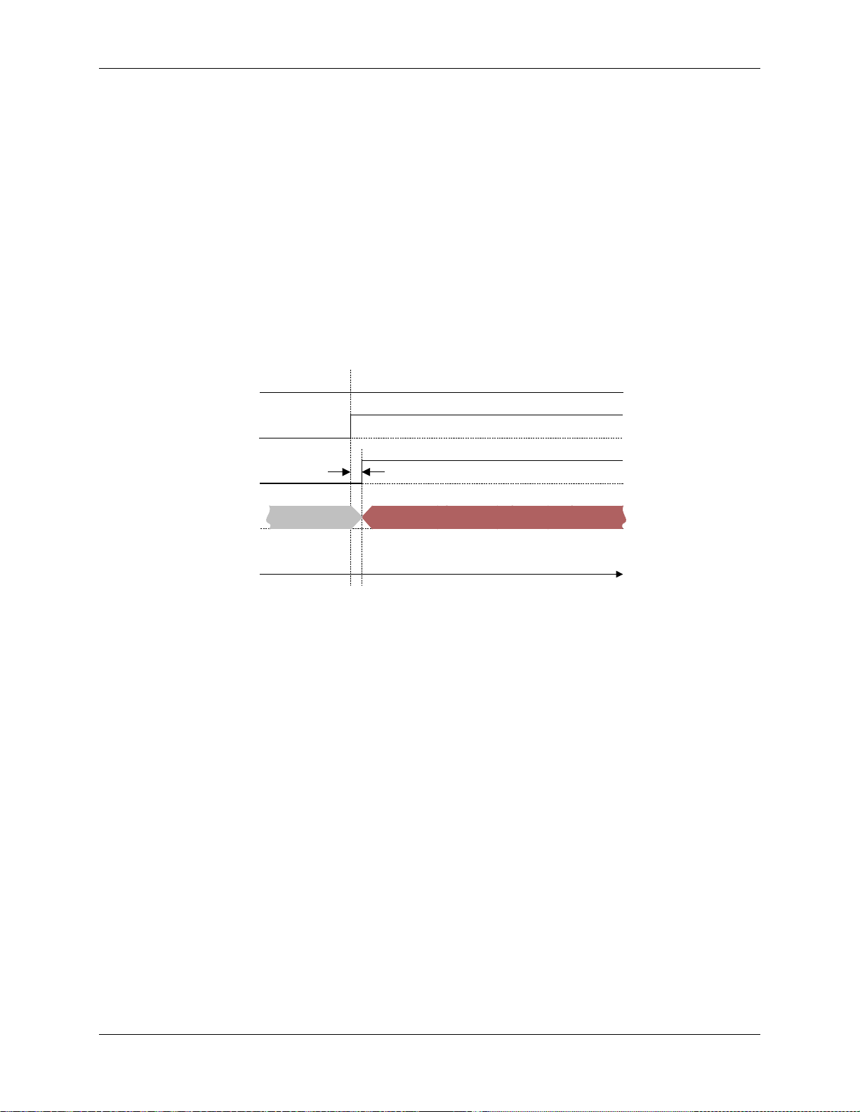
FDS 6531/6532 005 Data Sheet 71M6531D/F-71M6532D/F
time
System
Power
(V3P3SYS)
MPU Mode
PLL_OK
15 CK32
cycles
WAKE
LCD
PB or wake-
up timer
BROWNOUT
2.5 Wake-Up Behavior
As described above, the part will always wake up in MISSION mode when system power is restored.
Additionally, the part will wake up in BROWNO UT mode when PB rises (push button is pressed) or when
a timeout of the wake-up timer occurs.
2.5.1 Wake on PB
If the part is in SLEEP or LCD mode, it can be awakened by a rising edge on the PB pin. This pin is normally
pulled to GND and can be pulled high by a push but ton depression. Before the PB signal rises, the MPU
is in reset due to WAKE being low. When PB rises, WAKE rises and withi n three crystal cycles, the MPU
begins to execute. The MPU can determine whether the PB signal woke it up by checking the IE_PB flag.
Figure 25 shows the Wake Up timing.
For debouncing, the PB pin is monitored by a st ate machine operating from a 32 Hz clock. This circuit
will reject between 31 ms and 62 ms of noise. Detection hardware will ignore all transitions after the initi al
rising edge. This will continue until the MPU clear s t he IE_PB bit.
Figure 25: Wake Up Timing
2.5.2 Wake on Timer
If the part is in SLEEP or LCD mode, it can be awa kened by the wake-up timer. Until this timer times out,
the MPU is in reset due to WAKE being low. When the wake-up timer times out, the WAKE signal rises
and within three crystal cycles, the MPU begi ns to execute. The MPU can determine whether the timer
woke it by checking the AUTOWAKE interrupt flag (IE_WAKE).
The wake-up timer begins timing when the part enters LCD or SLEEP mode. Its duration is controlled by
WAKE_PRD[2:0] and WAKE_RES. WAKE_RES selects a timer LSB of either 1 minute (WAKE_RES = 1) or
2.5 seconds (WAKE_RES = 0). WAKE_PRD[2:0] selects a duration of from 1 to 7 LSBs.
The timer is armed by WAKE_ARM = 1. It must be armed at least three RTC cycles before SLEEP or
LCD_ONLY is initiated. Setting WAKE_ARM presets the timer with the values in WAKE_RES and WAKE_PRD
and readies the timer to start when the processor writ es to SLEEP or LCD_ONLY. The timer i s reset and
disarmed whenever the processor is awake. Thus, if it is desired to wake the MPU periodically (every 5
seconds, for example) the timer must be rearmed every time the MPU is awakened.
2.6 Data Flow
The data flow between the Comp ute En gine (CE) and the MPU is shown in
Figure 26. In a typical
application, the 32-bit CE sequentially processes the samples from the voltage inputs on pins IA, VA, IB
and VB, performing calculations to measure active power (Wh), reactive power (VARh), A
four-quadrant metering. These measurements are then accessed by the MPU, processed further and
output using the peripheral devices available t o the MPU.
Figure 26 illustrates the CE/MPU data flow.
v1.3 © 2005-2010 TERIDIAN Semiconductor Corporation 61
2
h and V2h for
Page 62
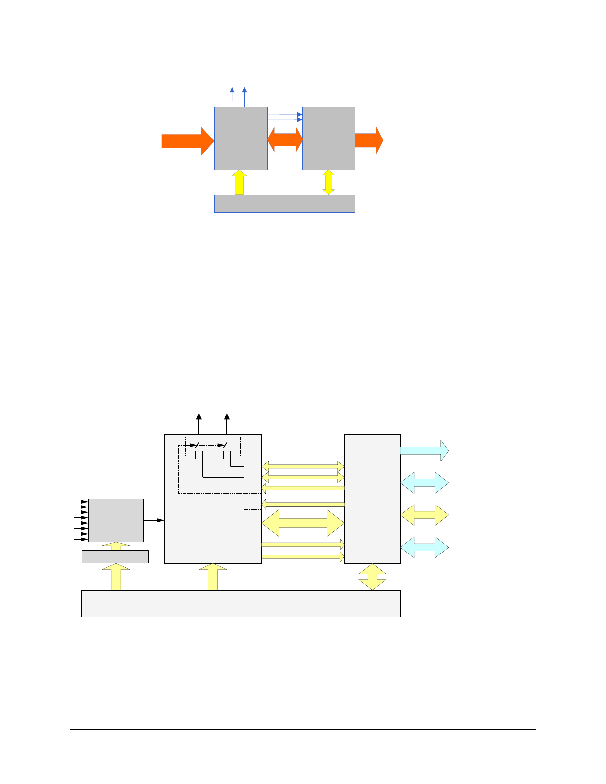
Data Sheet 71M6531D/F-71M6532D/F FDS 6531/6532 005
VARSUM
WSUM
APULSEW
APULSER
EXT PULSE
SAG CONTROL
DATA
DIO
XFER BUSY
SAMPLES
CE
MPU
INTERRUPTS
I/O RAM (Configuration RAM)
Mux Control
ADC
DISPLAY (Memory
mapped LCD
segments)
SERIAL
(UART0/1)
EEPROM
(I
2
C)
VAR
(DIO7)
PULSES
W (DIO6)
CE BUSY
CE
MPU
Pre
-
Processor
Post
-
Processor
IRQ
Processed
Metering
Data
Pulses
I/O RAM (Configuration RAM)
Samples
Data
Figure 26: MPU/CE Data Flow
2.7 CE/MPU Communication
Figure 27 shows the functional relationsh i ps between the CE and the MPU. The CE is controlled by the
MPU via shared registers in the I/O RAM and in RAM.
The CE outputs two interrupt signals to the MP U: CE _B US Y and XFER_BUSY, which are connected to
the MPU interrupt service inputs as external int errupts. CE_BUSY indicates that the CE is actively
processing data. This signal will occur once every multiplexer cycle. XFER_BUSY indicates that the CE
is updating data to the output region of the RAM. This will occur whenever the CE has finished generating
a sum by completing an accumulation interval determined by SUM_CYCLES[5:0] * PRE_SAMPS[1:0] samples.
Interrupts to the MPU occur on the falling edges of the XFER_BUSY and CE_BUSY signals.
Refer to Section 4.3 CE Interface Description for additional information on setting up the device using the
MPU firmware.
Figure 27: MPU/CE Communication
62 © 2005-2010 TERIDIAN Semiconductor Corporation v1.3
Page 63
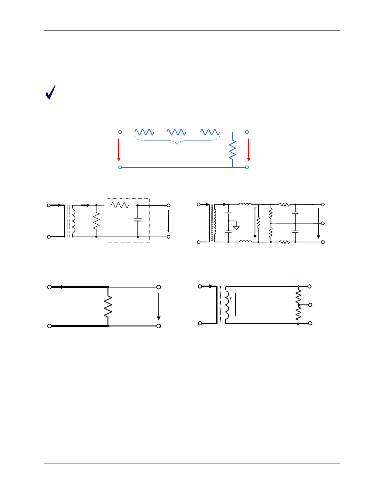
FDS 6531/6532 005 Data Sheet 71M6531D/F-71M6532D/F
VA = Vin * R
out
/(R
out
+ Rin)
V
in
R
in
R
out
VA
V
out
R
1/N
I
in
I
out
Filter
V3P3
IA
InP
InN
V3P3A
V
OUT
I
OUT
I
IN
R
1/N
V
DIFF
V
out
R
I
in
IA
V3P3
Vout = c*dIin/dt
V
out
1/N
I
in
IAN
IAP
V3P3A
3 Application Information
3.1 Connection of Sensors
Figure 28 through Figure 30 show how resistive dividers, current transformers, Rogowski coils and resistive
shunts are connected to the voltage and current inp uts of the 71M6531.
The analog input pins of the 71M65XX are design ed for sensors with low source impedance. RC
filters with resistance values higher than those im plemented in the Teridian Demo Boards should be
avoided.
Figure 28: Resistive Voltage Divider
Figure 29: CT with Single Ended (Left) and Differential Input (Right) Connection
Figure 30: Resistive Shunt (Left) and Rogowski Sensor (Right) Connection
3.2 Connecting 5-V Devices
All digital input pins of the 71M6531D/F and 71M6532D/F are compatible with external 5-V devices. I/O
pins configured as inputs do not require current-limiting resistors when they are connected to external 5 V
devices.
v1.3 © 2005-2010 TERIDIAN Semiconductor Corporation 63
Page 64
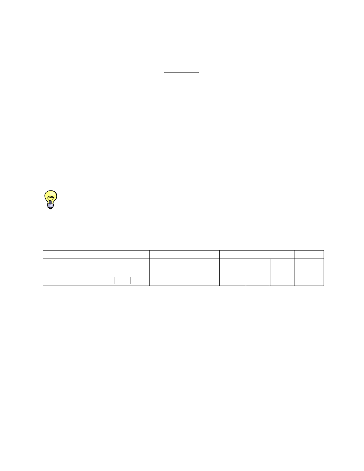
Data Sheet 71M6531D/F-71M6532D/F FDS 6531/6532 005
n
n
n
T
S
NTN
T +
−=))((
)40,22max(
10
)(
)()(
6
−−TTVNOM
TVNOMTVREF
3.3 Temperature Measurement
Measurement of absolute temperature uses the on-chip temperature sensor and applying the f ol l owing
formula:
In the above formula, T is the temperature in °C, N(T) is the ADC count at temperature T, N
count at 25°C, S
is the sensitivity in LSB/°C as stated in the Electrical Specifications and Tn is +25 °C.
n
is the ADC
n
It is recommended that temperature measurements be based on TEMP_RAW_X which is the sum of two
consecutive temperature readings, thus being hi gher by a factor of two than the raw sensor readings.
3.4 Temperature Compensation
3.4.1 Temperature Coefficients:
The internal voltage reference VREF is calibrat ed during device manufacture.
The temperature coefficient TC2 is given as a constant that represents typical component behavior (in
2
µV/°C
). TC1 (µV/°C) can be calculated for the indiv i dual chip from the contents of the TRIMT[7:0] I/O
RAM register. TC1 and TC2 allow compensation for variations of the reference voltage to within ± 40
PPM/°C.
2
Since TC1 and TC2 are given in µV/°C and µV/°C
(1.195V) has to be taken into account when transitioning to PPM/°C and PPM/°C
that PPMC = 26.84*TC1/1.195 and PPMC2 = 1374* TC2/1.195).
Close examination of the electrical specification (see Table 53) reveals that the achievable dev i ation is
not strictly ±40 PPM/°C over the whole temperature range: Only for t em peratures for which T-22 > 40 (i.e.
T > 62°C) or for which T-22 < -40 (i.e. T < -18°C), the data sheet states ±40 PPM/°C. For temperatures
between -18°C and +62°C, the error should be considered constant at ±1,600 PPM, or ±0.16%.
Parameter Condition Min Typ
VREF(T) deviation from VNOM(T)
, respectively, the value of the VREF voltage
2
. This means
-40 +40 PPM/ºC
Figure 31 shows this concept graphically . The “box” from -18°C to +62°C reflects the fact that it is impractical to measure the temperature coefficient of hi gh-quality references at small temperature ex cursions.
For example, at +25°C, the expected error would be ±3°C * 40 PPM/°C, or just 0.012%.
The maximum deviation of ±2520 PPM (or 0.252%) is reached at the temperature extremes. If the reference voltage is used to measure both voltage and current, the identical errors of ±0.252% add up to a
maximum Wh registration error of ±0.504%.
64 © 2005-2010 TERIDIAN Semiconductor Corporation v1.3
Table 53: VREF Definition for 6513H
Page 65
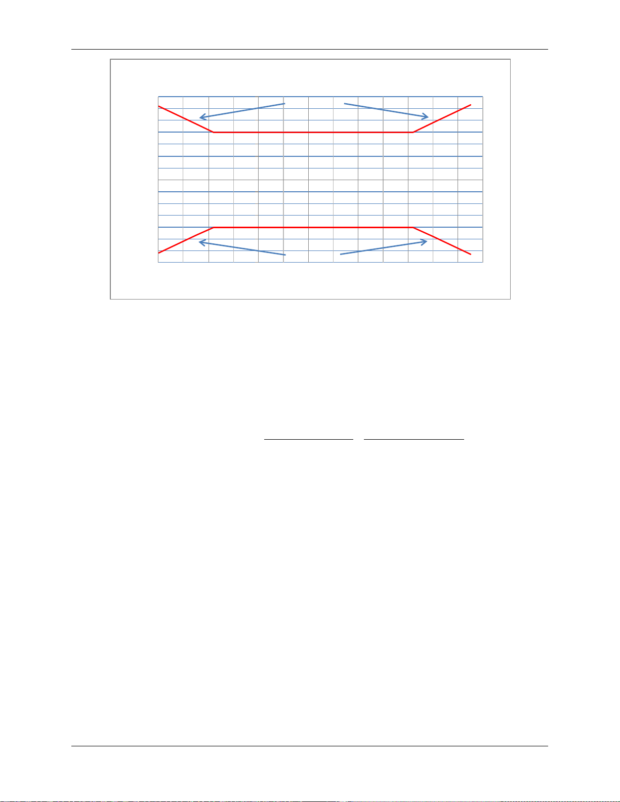
FDS 6531/6532 005 Data Sheet 71M6531D/F-71M6532D/F
23
2
14
2
2_
2
_
16385_
PPMCXTEMPPPMCXTEMP
ADJGAIN
⋅
+
⋅
+=
-2800
-2400
-2000
-1600
-1200
-800
-400
0
400
800
1200
1600
2000
2400
2800
-40 -20
0 20 40
60
80
Error Band (PPM) over Temperature (
°C)
±40 PPM/°C
±40 PPM/°C
Figure 31: Error Band for VREF over Temperature
3.4.2 Temperature Compensation for VREF
The bandgap temperature is used to digitally compensate the power outputs for the temperature dependence
of VREF, using the CE register GAIN_ADJ. Since the band gap amplifier is chopper-stabilized, the most
significant long-term drift mechanism in the v ol tage reference is removed.
The following formula is used to determine the GAIN_ADJ value of the CE. In this formula, TEMP_X is the
deviation from nominal or calibration temperature expressed in multiples of 0.1 °C:
3.4.3 System Temperature Compensation
In a production electricity meter, the 71M6531 or 71M6532D/F is not the only component contributing to
temperature dependency. A whole range of compone nts (e.g. current transformers, resistor dividers,
power sources, filter capacitors) will contribute temperature effects.
Since the output of the on-chip temperature sensor is accessible to the MPU, temperature compensation
mechanisms with great flexibility are possible. MPU access to GAIN_ADJ permits a system-wide temperature
correction over the entire meter rather than local to the chip.
3.4.4 Temperature Compensation for the RTC
In order to obtain accurate readings from t he RTC, the following procedure is recommended:
1. At the time of meter calibration, the crystal oscillator is calibrated using the RTCA_ADJ register in I/O
RAM to be as close to 32768 Hz as possible. The recommended procedure is to connect a highprecision frequency counter to the TMU X O UT pin and select 0x11 for TMUX[4:0]. This will generate
a 4-second pulse at TMUXOUT that can be used to trim RTCA_ADJ to the best value.
2. When the meter is in service, the MPU takes frequent temperature readings . If th e temper atur e
characteristics of the crystal are known, the t em perature readings can be used to modify the settings
for the I/O RAM registers PREG[16:0] and QREG[1:0] in order to keep the crystal frequency close to
32768 Hz.
3. After periods of operation under battery power, the temperature for the time the meter was not powered
can be estimated by averaging the temperatures before and after battery operation. Based on this, the
overall correction for the RTC time can be calculated and applied to the RTC after main power ret urns
to the meter.
v1.3 © 2005-2010 TERIDIAN Semiconductor Corporation 65
Page 66
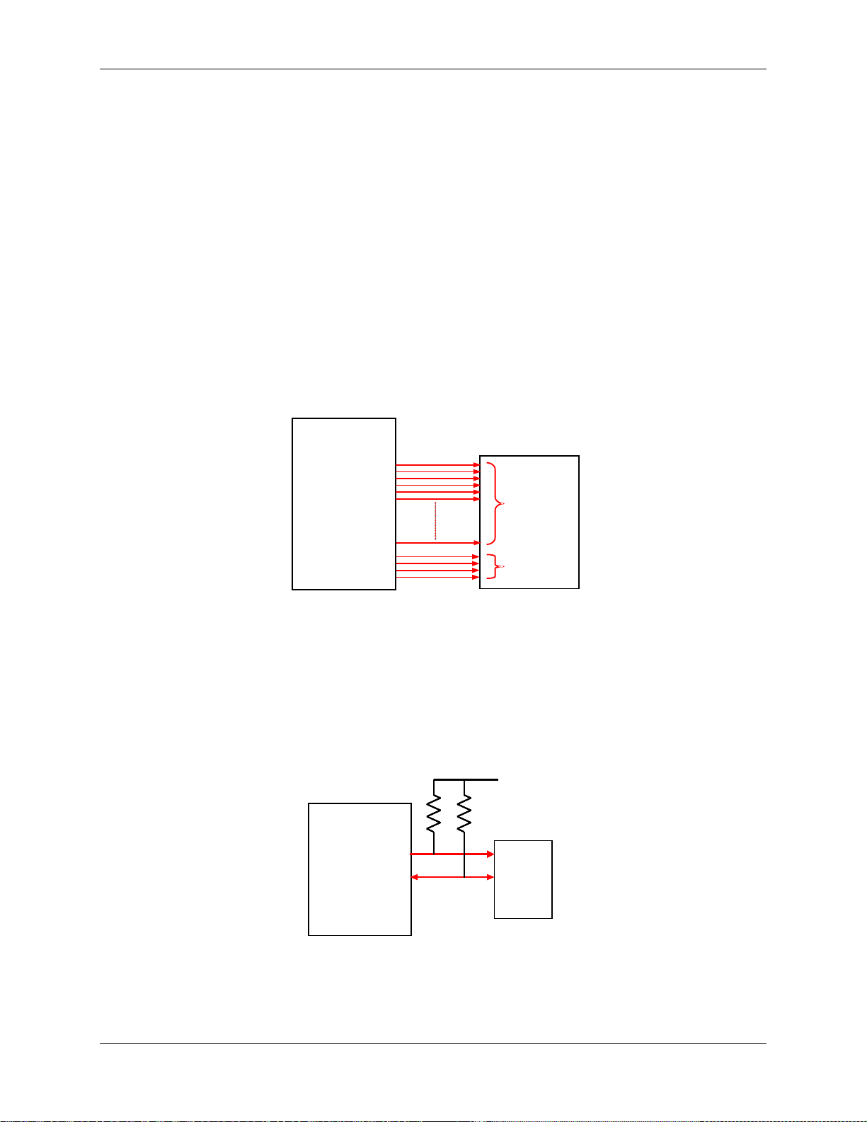
Data Sheet 71M6531D/F-71M6532D/F FDS 6531/6532 005
DIO4
DIO5
71M6531D/F
SCL
SDA
V3P3D
10 k
Ω
10 k
Ω
segments
71M6531D/F or 71M6532D/F
LCD
commons
3.5 Connecting LCDs
The 71M6531D/F and 71M6532D/F have an on-chip LCD controller cap able o f con trolling s tatic or
multiplexed LCDs. Figure 32 shows the basic connection for an LCD.
The following dedicated and multi-use pins can be assigned as LCD segment pins for the 71M6531D/ F:
• 12 dedicated LCD segment pins: SEG0 to SEG2, SEG7, SEG8, SEG12 to SEG18.
• 7 dual-function pins: SEG3/PCLK, SEG4/PSDO, SEG5/PCSZ, SEG6/PSDI, E_RXTX/SEG9,
E_TCLK/SEG10, and E_RST/SEG11.
• 14 combined DIO and segment pins: SEG24/DIO4 to SEG35/DIO15, SEG37/DIO17, SEG48/DIO28,
SEG49/DIO29 and SEG63/DIO43 to SEG66/DIO46.
The following dedicated and multi-use pins can be assigned a s LCD segments for the 71M6532D/F:
• 15 dedicated LCD segment pins: SEG0 to SEG2, SEG8, SEG12 - SEG18, SEG20 - SEG23.
• 9 dual-function pins: MUX_SYNC/SEG7, E_RXTX/SEG9, E_TCLK/SEG10, E_RST/SEG11,
SEG3/PCLK, SEG4/PSDO, SEG5/PCSZ, SEG6/PSDI.
• 43 combined DIO and segment pins, as described in section 1.5.8.
.
Figure 32: Connecting LCDs
3.6 Connecting I2C EEPROMs
I2C EEPROMs or other I2C compatible devices should be connected to the DIO pins DIO4 and DIO5, as
shown in Figure 33.
Pull-up resistors of roughly 10 kΩ to V3P3D (to ensure operat i on in BROWNOUT mode) should be used
for both SCL and SDA signals. The DIO_EEX[1:0] register in I/O RAM must be set to 01 in order to convert
the DIO pins DIO4 and DIO5 to I
2
C pins SCL and SDA.
71M6532D/F
2
Figure 33: I
C EEPROM Connection
EEPROM
66 © 2005-2010 TERIDIAN Semiconductor Corporation v1.3
Page 67
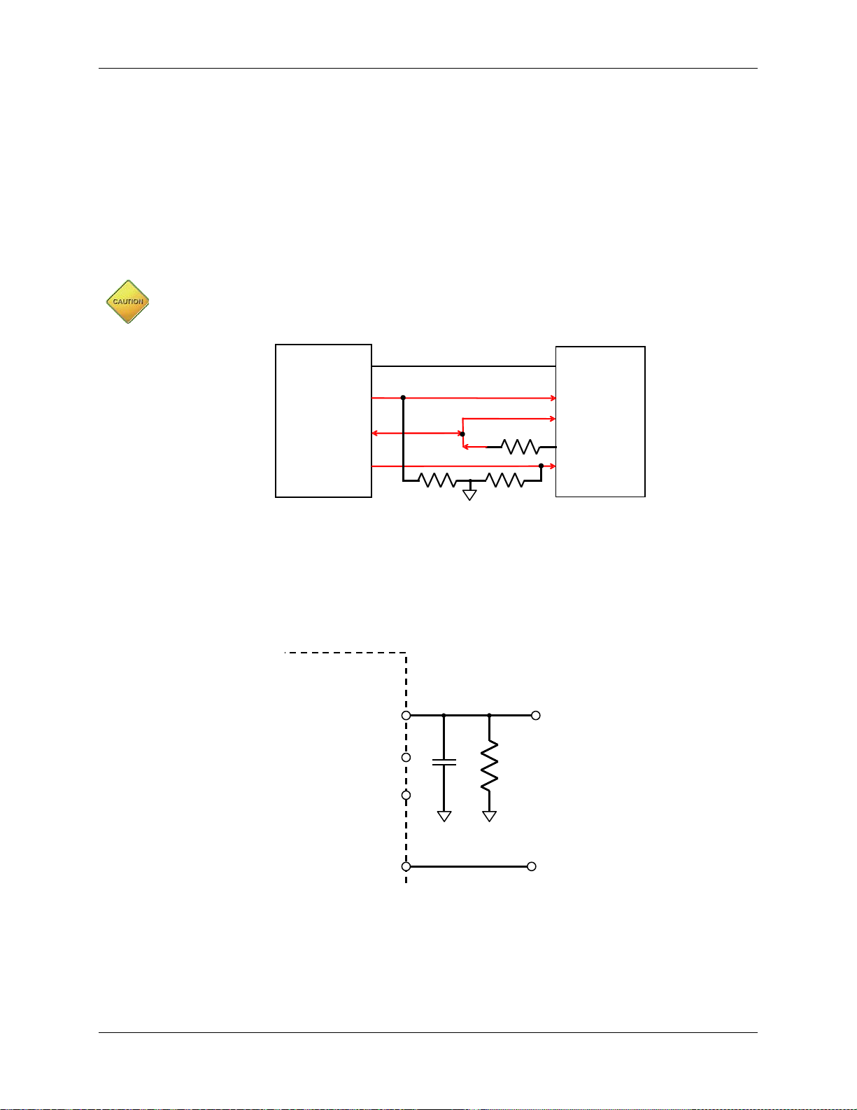
FDS 6531/6532 005 Data Sheet 71M6531D/F-71M6532D/F
TX
RX
71M6531D/F, 71M6532D/F
10 k
Ω
RX
TX
71M653X
EEPROM
100 kΩ
DIO4
DIO5
CLK
V3P3D
100 kΩ
CS
DIOn
DO
10 k
Ω
VCC
3.7 Connecting Three-Wire EEPROMs
µWire EEPROMs and other compatible device s should be connected to the DIO pins DIO4 and DIO5, as
shown in Figure 34 and described below:
• DIO5 connects to both the DI and DO pins of the t hree-wire device.
• The CS pin must be connected to a vacant DIO pin o f the 71M6531.
• In order to prevent bus contention, a 10 kΩ to resistor is used to separate the DI and DO signals.
• The CS and CLK pins should be pulled down with resistors to prevent operation of the three-wire device
on power-up, before the 71M6531 can establish a stable signal for CS and CLK.
• The DIO_EEX[1:0] register in I/O RAM must be set to 2 (b10) in order to convert the DIO pins DIO4
and DIO5 to µWire pins.
The µ-Wire EEPROM interface is only function al when MPU_DIV[2:0] = 000.
DI
Figure 34: Three-Wire EEPROM Connection
3.8 UART0 (TX/RX)
The UART0 RX pin should be pulled down by a 10 kΩ resistor and additionally pro tected by a 100 pF
ceramic capacitor, as shown in Figure 35.
100 pF
Figure 35: Connections for UART0
3.9 Optical Interface (UART1)
The OPT_TX and OPT_RX pins can be used for a regular ser ial in terface (by connecting a RS-232
transceiver for example), or they can be used to directly operate optical components (for example, an
infrared diode and phototransistor implementing a FLAG interface). Figure 36 shows the basic connections
for UART1. The OPT_TX pin becomes active when the I/O RAM register OPT_TXE is set to 00.
v1.3 © 2005-2010 TERIDIAN Semiconductor Corporation 67
Page 68
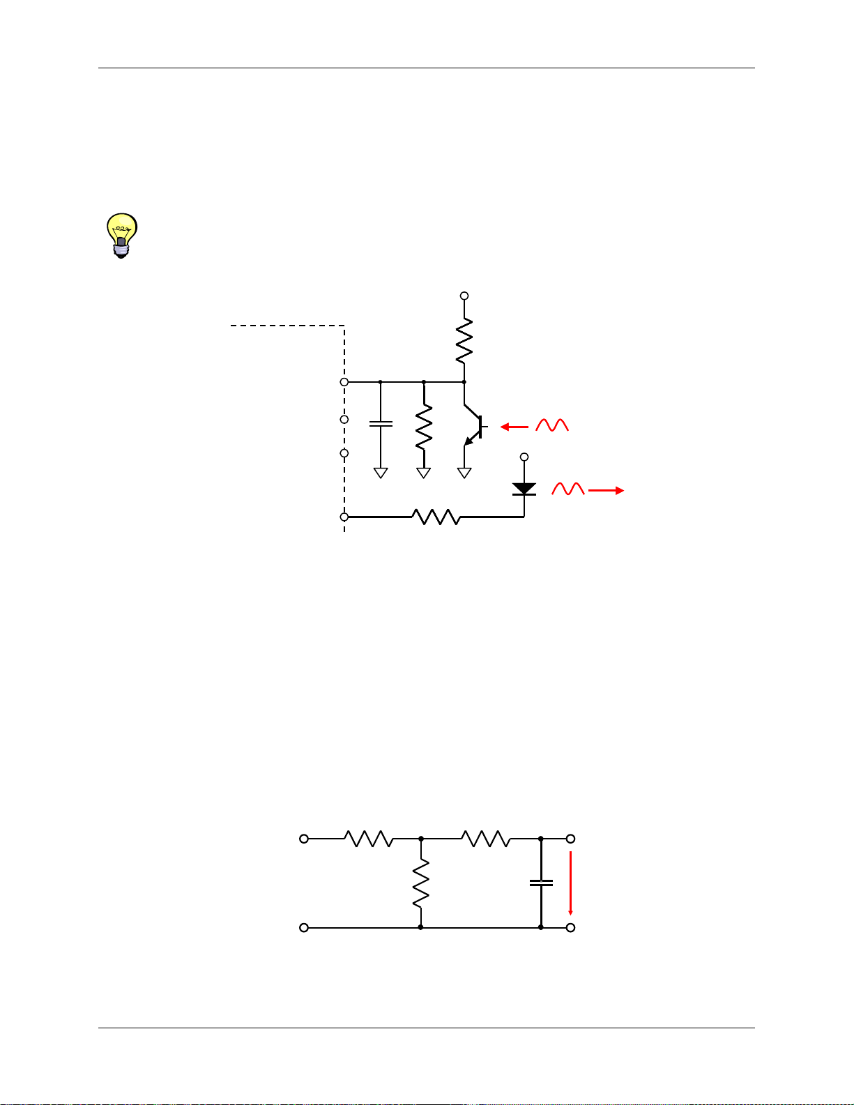
Data Sheet 71M6531D/F-71M6532D/F FDS 6531/6532 005
V3P3
R
2
V1
R
1
R
3
C
1
100pF
GND
16.9kΩ
20kΩ
R
2 R 1
71M6531D/F or 71M6532D/F
Phototransistor
10 kΩ
100 pF
The polarity of the OPT_TX and OPT_RX pins can be inverted with the configuration bits, OPT_TXINV
and OPT_RXINV, respectively.
The OPT_TX output may be modulated at 38 kHz when system power is present. Modulation is not
available in BROWNOUT mode. The OPT_TXMOD bit enables modulation. The duty cycle is controlled
by OPT_FDC[1:0], which can select 50%, 25%, 12.5% and 6.25% duty cycle. A 6.25% duty cycle means
OPT_TX is low for 6.25% of the period. The OPT_RX pin uses digital signal thresholds. It may need an
analog filter when receiving modulated optical signals.
With modulation, an optical emitter can be oper ated at higher current than nominal, enabling it to
increase the distance along the optical path.
If operation in BROWNOUT mode is desired, the external components should be connected to V3P3D.
V3P3SYS
OPT_RX
V3P3SYS
LED
OPT_TX
Figure 36: Connection for Optical Components
3.10 Connecting the V1 Pin
A voltage divider should be used to establish that V 1 is in a saf e range when the meter is in MISSION
mode (see Figure 37). V1 must be lower than 2.9 V in all cases in order to keep the hard ware watchdog
timer enabled. The resistor divider ratio must be chosen so that V1 crosses the VBIAS threshold wh en
V3P3 is near the minimum supply voltage (3.0 VDC). A series resistor (R3) provides additional hysteresis,
and a capacitor to ground (C1) is added for enhanced EMC immunity.
The amount of hysteresis depends on the choice of R1 an d R3: If V1 < VBIAS, approximately 1 µA will
flow into the on-chip V1 comparator causing a voltage drop. If V1 ≥ VBIAS, almost no current will flow
into the comparator. The voltage drop will require V3P3 to be slightly higher for V1 to cross the V BIAS
threshold when V3P3 is rising as compared to when V3P3 is falling. Maintaining sufficient hyst eresis
helps to eliminate rapid mode changes which may occur in cases where the power supply is unstable with
V1 close to the VBIAS threshold point.
68 © 2005-2010 TERIDIAN Semiconductor Corporation v1.3
Figure 37: Voltage Divider for V1
Page 69
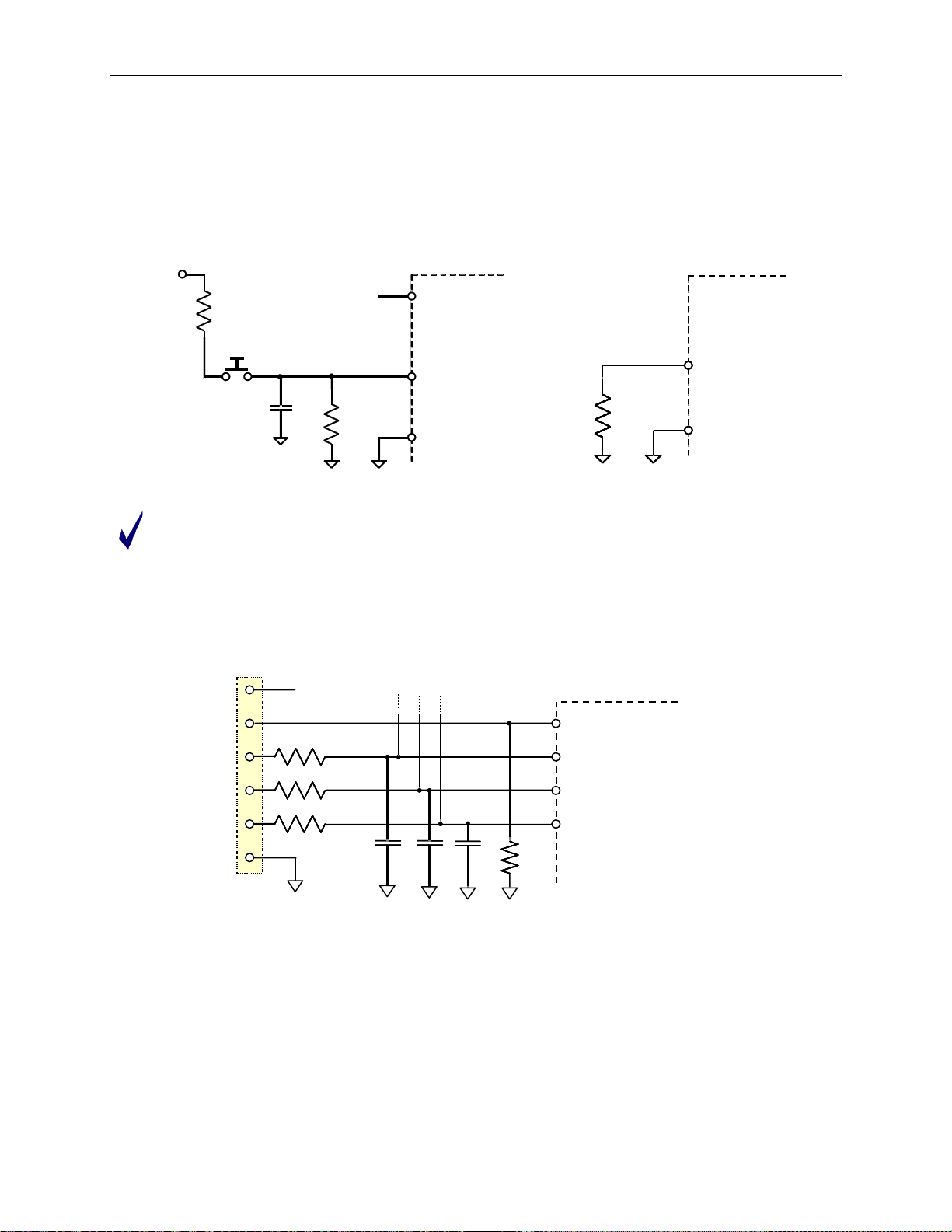
FDS 6531/6532 005 Data Sheet 71M6531D/F-71M6532D/F
R
1
RESET
71M6533
DGND
100Ω
R
1
RESET
71M6533
DGND
100Ω
E_RST
71M6531D/F
E_TCLK
62
Ω
62 Ω
62 Ω
22 pF
22 pF
22 pF
LCD Segments
ICE_E
(optional)
R
1
RESET
GNDD
R
2
VBAT/
V3P3D
Reset
Switch
1k Ω 0.1µF
10k
Ω
71M6531D/F
71M6531D/F
3.11 Connecting the Reset Pi n
Even though a functional meter will not necessarily need a reset switch, it is useful to have a reset pushbutton for prototyping as shown in Figure 38, left side. The RESET signal may be sourced from V3P3SYS
(functional in MISSION mode only), V3P3D (MISSI O N and BROWNOUT modes), or VBAT (all modes, i f
a battery is present), or from a combination of these sources, depending on the application.
For a production meter, the RESET pin should be protected by the by the external components shown in
Figure 38, right side. R1 should be in the range of 100 Ω and mounted as closely as possible to the IC.
V3P3D
71M6532D/F
71M6532D/F
Figure 38: External Components for the RESET Pin: Push-button (Left), Production Circuit (Right)
Since the 71M6531 generates its own power-on reset, a reset butt on or circu itry, as sho wn in Figure 38,
is only required for test units and prototypes.
3.12 Connecting the Em ulator Port Pins
Even when the emulator is not used, small shunt capacitors to ground (22 pF) should be used for protection
from EMI as illustrated in Figure 39. Production boards should have the ICE_E pi n connected to ground.
V3P3D
E_RXT
71M6532D/F
Figure 39: External Components for the Emulator Interface
3.13 Connecting a Batt ery
It is important that a valid voltage is connecte d to the VBAT pin at all times. For meters without a battery,
VBAT should be connected directly to V3P3SYS. Designs for meters with batteries need to ensure that
the meter functions even when the battery v ol tage decreases below the specified voltage for VBAT. This
can be achieved by connecting a diode from V3P3SYS to VBAT. However, the battery test will yield
inaccurate results if that technique is used, since the voltage at V3P3SYS will feed current to the VBAT
pin. A better solution is shown in Figure 40: During the battery test, a DIO pin is activated as an output
and applies a low voltage to the anode of the di ode. This prevents the voltage at the power supply t o influence the voltage at the VBAT pin.
v1.3 © 2005-2010 TERIDIAN Semiconductor Corporation 69
Page 70
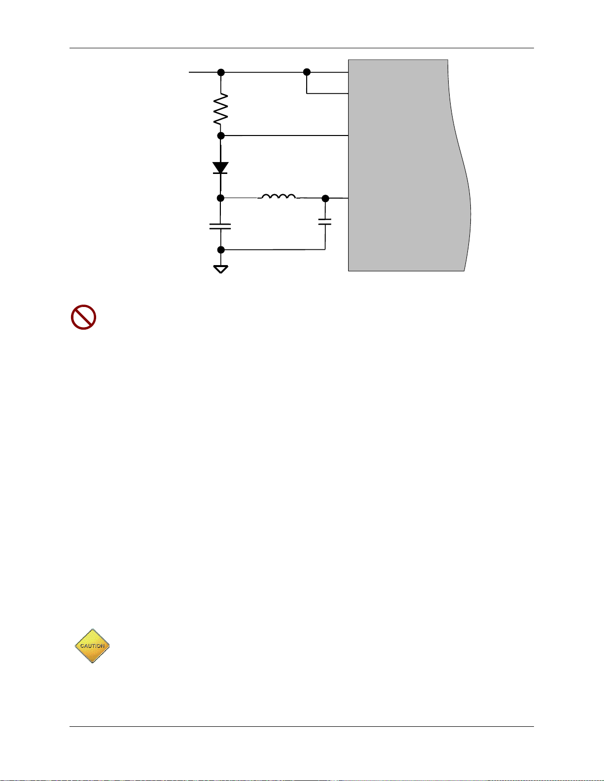
Data Sheet 71M6531D/F-71M6532D/F FDS 6531/6532 005
71M6531/71M6532
V3P3A
DIO
Power
Supply
V3P3SYS
VBAT
Battery or
Super-Cap
+
-
Figure 40: Connecting a Battery
As mentioned in section 2.3, meters equi pped with batteries need to contain code that transitions
the chip to SLEEP mode as soon as the battery is at tached in production. Otherwise, remaining
in BROWNOUT mode would add unnecessary drain to the battery.
3.14 Flash Programming
Operational or test code can be programmed into the flash memory using either an in-circuit emulator or
the Flash Programmer Module (TFP2) available from Teridian. The flash programming procedure uses
the E_RST, E_RXTX and E_TCLK pins. The FL_BANK[2:0] register must be set to the value corresponding
to the bank that is being programmed.
3.15 MPU Firmware
All application-specific MPU functions mentioned in the Application Information section are featured in the
demonstration source code supplied by T eridi an. The code is available as part of the Demonstration Kit
for the 71M6531D/F and 71M6532D/F. The Demonstration Kits come with the 71M6531D/F or 71M6532D/F
preprogrammed with demo firmware and mounted on a functional sample meter Demo Board. The Demo
Boards allow for quick and efficient evaluat i on of the IC without having to write firmware or hav i ng to
supply an in-circuit emulator (ICE).
3.16 Crystal Oscillator
The oscillator drives a standard 32.768 kHz watch crystal. The oscillator has been designed specifically
to handle these crystals and is compatible with their high impedance and limited power handling capability.
The oscillator power dissipation is very low to maxi m ize the lifetime of any battery backup device attached
to VBAT.
Board layouts with minimum capacitance f rom XIN to XOUT will require less battery current. Good
layouts will have XIN and XOUT shielded from each other.
For best rejection of electromagnetic interference, connect the crystal body and the ground
terminals of the two crystal capacitors to GNDD through a ferrite bead. No external resistor
should be connected across the crystal, since the oscillator is self-biasing.
70 © 2005-2010 TERIDIAN Semiconductor Corporation v1.3
Page 71

FDS 6531/6532 005 Data Sheet 71M6531D/F-71M6532D/F
3.17 Meter Calibration
Once the Teridian 71M6531D/F or 71M6532D/F energy meter device has been installed in a meter system,
it must be calibrated. A complete calibration includes the following:
• Calibration of the metrology section, i.e. calibration for tolerances of the current sensors, voltage dividers
and signal conditioning components as well as of the internal reference voltage (VREF).
• Establishment of the reference temperature (Section 3.3) for temperature measurement and temperature
compensation (Section 3.4).
• Calibration of the battery voltage measurement (Section 1.5.13).
• Calibration of the oscillator frequency (Section 1.5.3) and temperature compensation for the RTC
(Section 3.4.4).
The metrology section can be calibrated using t he gain and phase adjustment factors accessible to the
CE. The gain adjustment is used to compensate for tolerances of components used for signal conditioning,
especially the resistive components. Phase a djustment is pr ovided to comp ensate for phase shi fts
introduced by the current sensors or by the effects of reactive power supplies.
Due to the flexibility of the MPU firmware, any calibration method, such as calibration based o n energy, or
current and voltage c an be i mple mented. It is also po ssible to i mplement segment -wise calibration (depending
on current range).
The 71M6531D/F and 71M6532D/F support common industry standard calibration techniques, such as singlepoint (energy-only), multi-point (energy, Vrms, Irms) and auto-calibration.
v1.3 © 2005-2010 TERIDIAN Semiconductor Corporation 71
Page 72
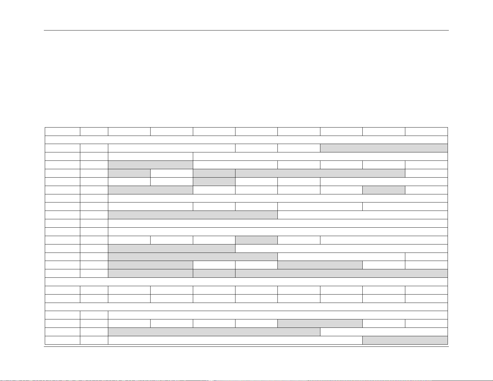
Data Sheet 71M6531D/F-71M6532D/F FDS 6531/6532 005
Name
Addr
Bit 7
Bit 6
Bit 5
Bit 4
Bit 3
Bit 2
Bit 1
Bit 0
CE1
2001
PRE_SAMPS[1:0]
SUM_CYCLES[5:0]
COMP0
2003
U
PLL_OK
U U U U U
COMP_STAT
CONFIG0
VREF_CAL
PLS_INV
CKOUT_E
VREF_DIS
MPU_DIV[2:0]
VERSION
2006
VERSION[7:0]
CE3
209D
U
MUX_DIV[3:0]
CE5
20A8
CE_LCTN[7:0]
WAKE
WAKE_ARM
SLEEP
LCD_ONLY
WAKE_RES
WAKE_PRD[2:0]
ANACTRL
20AB
R (0000)
LCD_DAC[2:0]
CHOP_I_EN‡
CONFIG4
20AD U R (0)
R (0)
U
R (0)
R (0)
Interrupts and WD Timer
INTBITS
SFR F8
WD_RST
INT6
INT5
INT4
INT3
INT2
INT1
INT0
IFLAGS
IE_PLLFALL
IE_PLLRISE
IE_WAKE
IE_PB
IE_FWCOL1
IE_FWCOL0
IE_RTC
IE_XFER
Flash Memory:
ERASE
SFR 94
FLSH_ERASE[7:0]
FL_BANK
SFR B6
U
FLBANK[2:0]
4 Firmware Interface
4.1 I/O RAM and SFR Map – Functional Order
In Table 54, unimplemented (U) and reserved (R) bits are shaded in light gray. Unimplemented bits have no memory storage, writing them has no
effect, and reading them always returns zero. Reserved bits may be in use and should not be changed from the values given in parentheses.
Writing values other than those shown in pare nthesis to reserved bits may have undesirable side ef fects and must be avoided.
Non-volatile bits are shaded in dark gray. Non-volatile bits are backed-up during power failures if the system includes a battery connected to t he
VBAT pin.
This table lists only the SFR registers that are not generic 8051 SFR registers. Bits marked with † apply to the 71M 6531D/F only, bits marked with
‡ apply to the 71M6532D/F only and should be 0 f or the other device.
Table 54: I/O RAM Map in Functional Order
Configuration:
CE0
2000
EQU[2:0] CE_E CE10MHZ
U
CE2
CONFIG1
CONFIG2
CE4
TMUX
CONFIG3
FLSHCTL
PGADR
2002
2004
2005
2007
20A7
20A9
20AA
20AC
SFR E8
SFR B2
SFR B7
U
U U
OPT_TXE[1:0] EX_PLL EX_FWCOL FIR_LEN[1:0] OPT_FDC[1:0]
U
U
:
PREBOOT SECURE WRPROT_BT WRPROT_CE
CHOP_E[1:0] RTM_E WD_OVF EX_RTC EX_XFR
U
ECK_DIS M26MHZ ADC_E MUX_ALT
BOOT_SIZE[7:0]
U
TMUX[4:0]
SEL_IBN‡ CHOP_IB‡
FLSH_PGADR[5:0]
U
U
U
SEL_IAN‡ CHOP_IA‡
FLSH_MEEN FLSH_PWE
M40MHZ
U
72 © 2005-2010 TERIDIAN Semiconduc tor Corporation v1.3
Page 73
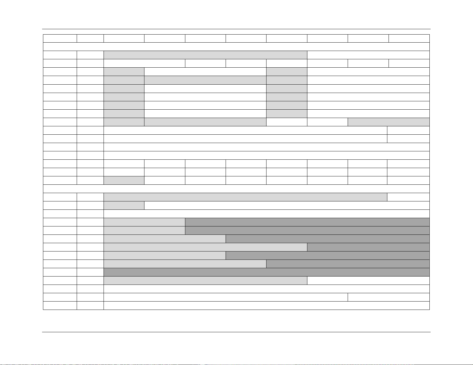
FDS 6531/6532 005 Data Sheet 71M6531D/F-71M6532D/F
Name
Addr
Bit 7
Bit 6
Bit 5
Bit 4
Bit 3
Bit 2
Bit 1
Bit 0
DIO3
DIO_R5[2:0]
DIO_R4[2:0]
DIO5
DIO_R9[2:0]
DIO_R8[2:0]
DIO6
DIO_R11[2:0]
DIO_R10[2:0]
DIO_PX
DIO_PY
DIO7
DIO_0[7:1]
DIO_0[0]†
DIO8
DIO_DIR0[7:1]
DIO_DIR0[0]†
DIO9
DIO_1[7:0] (Port 1)
DIO10
DIO_DIR1[7:0]
DIO11
DIO_2[7]‡
DIO_2[6]‡
DIO_2[5]‡
DIO_2[4] ‡
DIO_2[3] ‡
DIO_2[2] ‡
DIO_2[1]
DIO_2[0]‡
Real Time Clock:
RTCCTRL
RST_SUBSEC
SUBSEC1
SUBSEC[7:0]
RTC0
RTC_SEC[5:0]
RTC2
RTC_HR[4:0]
RTC5
RTC_MO[3:0]
RTC6
RTC_YR[7:0]
RTCADJ_M
PREG[13:6]
RTCADJ_L
PREG[5:0]
QREG[1:0]
Digital I/O:
20AF U
DIO0
DIO1
DIO2
2008
2009
200A
DIO_EEX[1:0] OPT_RXDIS OPT_RXINV DIO_PW DIO_PV OPT_TXMOD OPT_TXINV
U
DIO_R1[2:0]†
U U U
200B U
DIO4
200C
U
DIO_R7[2:0]
200D U
200E U
200F R(0) R (0) U
U
U
U
U
U
DIO_RRX[2:0]
DI_RPB[2:0]
DIO_R2[2:0]
DIO_R6[2:0]
U
SFR 80
SFR A2
SFR 90
SFR 91
DIO12
DIO13
SFR A0
SFR A1
SFR B0
DIO_DIR2[7] ‡ DIO_DIR2[6] ‡ DIO_DIR2[5] ‡ DIO_DIR2[4] ‡ DIO_DIR2[3] ‡ DIO_DIR2[2] ‡ DIO_DIR2[1] DIO_DIR2[0] ‡
R(0)
DIO_3[6]‡ DIO_3[5] DIO_3[4]† DIO_3[3] ‡ DIO_3[2] ‡ DIO_3[1] ‡ DIO_3[0] ‡
2010 U
RTCA_ADJ
2011
U
RTCA_ADJ[6:0]
2014
2015 U
RTC1
2016
U
RTC_MIN[5:0]
2017 U
RTC3
RTC4
2018
2019
U
U
RTC_DATE[2:0]
RTC_DAY[2:0]
201A U
201B
RTCADJ_H
201C
U
PREG[16:14]
201D
201E
WE
201F RTC write protect register
v1.3 © 2005-2010 TERIDIAN Semiconductor Corporation 73
Page 74
Data Sheet 71M6531D/F-71M6532D/F FDS 6531/6532 005
Name
Addr
Bit 7
Bit 6
Bit 5
Bit 4
Bit 3
Bit 2
Bit 1
Bit 0
LCD Display Interface:
LCDX
MUX_SYNC_E
BME
LCDY
LCD_Y
LCD_E
LCD_MODE[2:0]
LCD_CLK[1:0]
LCD_MAP0
LCD_BITMAP[31:24]
LCD_BITMAP
LCD_BITMAP
LCD_BITMAP
LCD_BITMAP
LCD_BITMAP
LCD_BITMAP
LCD_BITMAP
LCD_BITMAP
LCD_BITMAP
LCD_BITMAP
LCD_MAP6
LCD0
LCD_SEG42[3:0]‡
LCD_SEG0[3:0]
LCD1
2031
LCD_SEG43[3:0]‡
LCD_SEG1[3:0]
LCD2
2032
LCD_SEG2[3:0]
LCD4
2034
LCD_SEG46[3:0]‡
LCD_SEG4[3:0]
LCD7
LCD_SEG49[3:0]
LCD_SEG7[3:0]
LCD8
LCD_SEG50[3:0]‡
LCD_SEG8[3:0]
LCD9
…
…
…
…
LCD18
LCD_SEG60[3:0]‡
LCD_SEG18[3:0]
LCD19
LCD_SEG61[3:0]‡
LCD_SEG19[3:0]
LCD21
LCD_SEG63[3:0]
LCD_SEG21[3:0]‡
LCD24
LCD_SEG66[3:0]†
LCD_SEG24[3:0]
LCD25
LCD_SEG67[3:0]‡
LCD_SEG25[3:0]
LCD26
LCD_MAP1
LCD_MAP2
LCD_MAP3
LCD_MAP4
LCD_MAP5
LCD3
LCD5
LCD6
2020
R (0) R (0) U
2021 U
2023
2024
2025
2026
2027
2028
[39]‡
[63]
[71]‡
[38]‡
LCD_BITMAP
[62]‡
LCD_BITMAP
[70]‡
[37]
U
LCD_BITMAP
[61]‡
LCD_BITMAP
[69]‡
[36]‡
LCD_BITMAP[47:40]‡
LCD_BITMAP
[60]‡
LCD_BITMAP
[68]‡
2029 U
2030
U
2033
2035
2036
LCD_SEG45[3:0]‡ LCD_SEG3[3:0]
LCD_SEG47[3:0]‡ LCD_SEG5[3:0]
LCD_SEG48[3:0]† LCD_SEG6[3:0]†
2037
2038
2039
U
[35]
LCD_BITMAP
[67]‡
[34]
LCD_BITMAP
[50]‡
LCD_BITMAP
[66]†
LCD_SEG9[3:0]
[33]
LCD_BITMAP
[49]
U
LCD_BITMAP
[65]
[32]
LCD_BITMAP
[48]†
LCD_BITMAP
[64]
LCD17
LCD20
LCD22
LCD23
74 © 2005-2010 TERIDIAN Semiconductor Corporation v1.3
2041
2042
2043
2044
2045
2046
2047
2048
2049
204A
U
LCD_SEG62[3:0]‡ LCD_SEG20[3:0]‡
LCD_SEG64[3:0] LCD_SEG22[3:0]‡
LCD_SEG65[3:0] LCD_SEG23[3:0]‡
LCD_SEG68[3:0]‡ LCD_SEG26[3:0]
LCD_SEG17[3:0]
Page 75
FDS 6531/6532 005 Data Sheet 71M6531D/F-71M6532D/F
Name
Addr
Bit 7
Bit 6
Bit 5
Bit 4
Bit 3
Bit 2
Bit 1
Bit 0
LCD27
204B
LCD28
204C
LCD_SEG70[3:0]‡
LCD_SEG28[3:0]
LCD29
204D
LCD30
204E
…
…
…
…
LCD33
2053
U
LCD37
LCD_SEG37[3:0]
…
…
…
LCD41
LCD_SEG41[3:0]‡
205A
RTM:
RTM0H
RTM0[9:8]
2061
RTM1L
RTM1[7:0]
2064
U
RTM3H
2066
U
RTM3[9:8]
2067
SPI Interface:
SPI…
2070
SPE
U
SP_ADL
SP_ADDR[7:0]
Pulse Generator:
PLS_I
2081
PLS_INTERVAL[7:0]
ADC MUX:
SLOT1
2091
SLOT3_SEL
SLOT2_SEL
SLOT4
2094
R
R
LCD_SEG69[3:0]‡ LCD_SEG27[3:0]†
LCD_SEG71[3:0]‡ LCD_SEG29[3:0]
U
LCD_SEG30[3:0]
LCD_SEG35[3:0]
LCD36
2054
U
LCD_SEG36[3:0]‡
2055 U
LCD38
2056
U
LCD_SEG38[3:0]‡
…
2059 U
LCD_BLNK
LCD_BLKMAP19[3:0] LCD_BLKMAP18[3:0]
2060 U
RTM0L
RTM1H
2062
U
RTM0[7:0]
RTM1[9:8]
2063
RTM2H
RTM2L
2065
RTM2[7:0]
RTM2[9:8]
RTM3L
SP_CMD
SP_ADH
PLS_W
SLOT0
SLOT2
SLOT3
v1.3 © 2005-2010 TERIDIAN Semiconductor Corporation 75
2071
2072
2073
2080
2090
2092
2093
RTM3[7:0]
SP_CMD[7:0]
SP_ADDR[15:8]
PLS_MAXWIDTH[7:0]
SLOT1_SEL SLOT0_SEL
R R
R R
Page 76
Data Sheet 71M6531D/F-71M6532D/F FDS 6531/6532 005
Name
Addr
Bit 7
Bit 6
Bit 5
Bit 4
Bit 3
Bit 2
Bit 1
Bit 0
SLOT5
SLOT6
SLOT7
SLOT8
SLOT9
2096
2097
2098
2099
209A
SLOT1_ALTSEL SLOT0_ALTSEL
SLOT3_ALTSEL SLOT2_ALTSEL
R R
R R
R R
SPI Interrupt:
SPI0
SPI1
20B0
20B1
U
U
IEN_SPI
SPI_FLAG
General-Purpose Nonvolatile Registers:
GP0
20C0
GPO[7:0]
… … …
GP7
VERSION
20C7
20C8
GP7[7:0]
VERSION[7:0]
Serial EEPROM:
EEDATA
EECTRL
SFR 9E
SFR 9F
EEDATA[7:0]
EECTRL[7:0]
† 71M6531D/F only
‡ 71M6532D/F only
U
U
IEN_WD_NROVF
WD_NROVF_FLAG
76 © 2005-2010 TERIDIAN Semiconductor Corporation v1.3
Page 77
FDS 6531/6532 005 Data Sheet 71M6531D/F-71M6532D/F
Name
Location
Reset
Wake
Dir
Description
4.2 I/O RAM Description – Alphabetical Order
The following conventions apply to the descriptions in this table:
• Bits with a W (write) direction are written by the MPU into configuration RAM. Typically, they are initial ly stored in flash memory and copied to
the configuration RAM by the MPU. Some of the more frequently programmed bits are mapped to the MPU SFR memory space. The remaining
bits are mapped to 2xxx.
• Bits with a R (read) direction can be read by the MPU.
• Columns labeled Reset and Wake describe the bit values upon reset and wake, respectively. “NV” in the Wake column means the bit is powered
by the nonvolatile supply and is not initialized. LCD-related registers labeled “L” retain data upon transition from LCD mode to BROWNOUT
mode and vice versa, but do not retain data in SLE E P mode. “–“ means that the value is undefined.
• Write-only bits will return zero when the y are read.
Table 55: I/O RAM Description - Alphabetical
ADC_E
BME
BOOT_SIZE[7:0]
CE10MHZ
CE_E
CE_LCTN[7:0]
CHOP_E[1:0]
CHOP_IA
CHOP_IB
CHOP_I_E
CKOUT_E
v1.3 © 2005-2010 TERIDIAN Semiconductor Corporation 77
2005[3] 0 0 R/W Enables ADC and VREF. When disabled, removes bias current.
Battery Measure Enable. When set, a load current is immediately applied to the battery
2020[6] 0 – R/W
20A7[7:0] 01 01 R/W
2000[3] 0 0 R/W
2000[4] 0 0 R/W CE enable.
20A8[4:0] 31 31 R/W CE program location. The starting address for the CE program is 1024*CE_LCTN.
2002[5:4] 0 0 R/W
20AC[0] 0 0
20AC[4] 0 0
20AB[0] 0 0
2004[4]
0 0
R/W
R/W
R/W This bit must be set to enable chop mode for the current channels (71M6532D/F only).
R/W
and it is connected to the ADC to be measured on Alternative Mux Cycles. See the
MUX_ALT bit.
End of space reserved for boot program. The ending address of the boot region is
1024*BOOT_SIZE.
CE clock select. When set, the CE is clocked at 10 MHz. Otherwise, the CE clock
frequency is 5 MHz.
Chop enable for the reference bandgap cir cuit. T he value of CHOP will change on the
rising edge of MUXSYNC according to the value in CHOP_E[1:0]:
00 = toggle, except at the mux sync edge at the end of SUMCYCLE, an alternative
MUX frame is automatically inserted at the end of each accumulation interval.
01 = positive.
10 = reversed.
11 = toggle, no alternative MUX frame is inserted
This bit enables chop mode for the IA current channel (71M6532D/F only ). CHOP_I_E
must be set also.
This bit enables chop mode for the IB current channel (71M6532D/F only). CHOP_I_E
must be set also.
Control bit for the SEG19/CKOUT pin:
0: The pin is the SEG19 LCD driver
1: The pin is the CK_FIR output (5 MHz in mission mode, 32 kHz in brownout mode)
Page 78
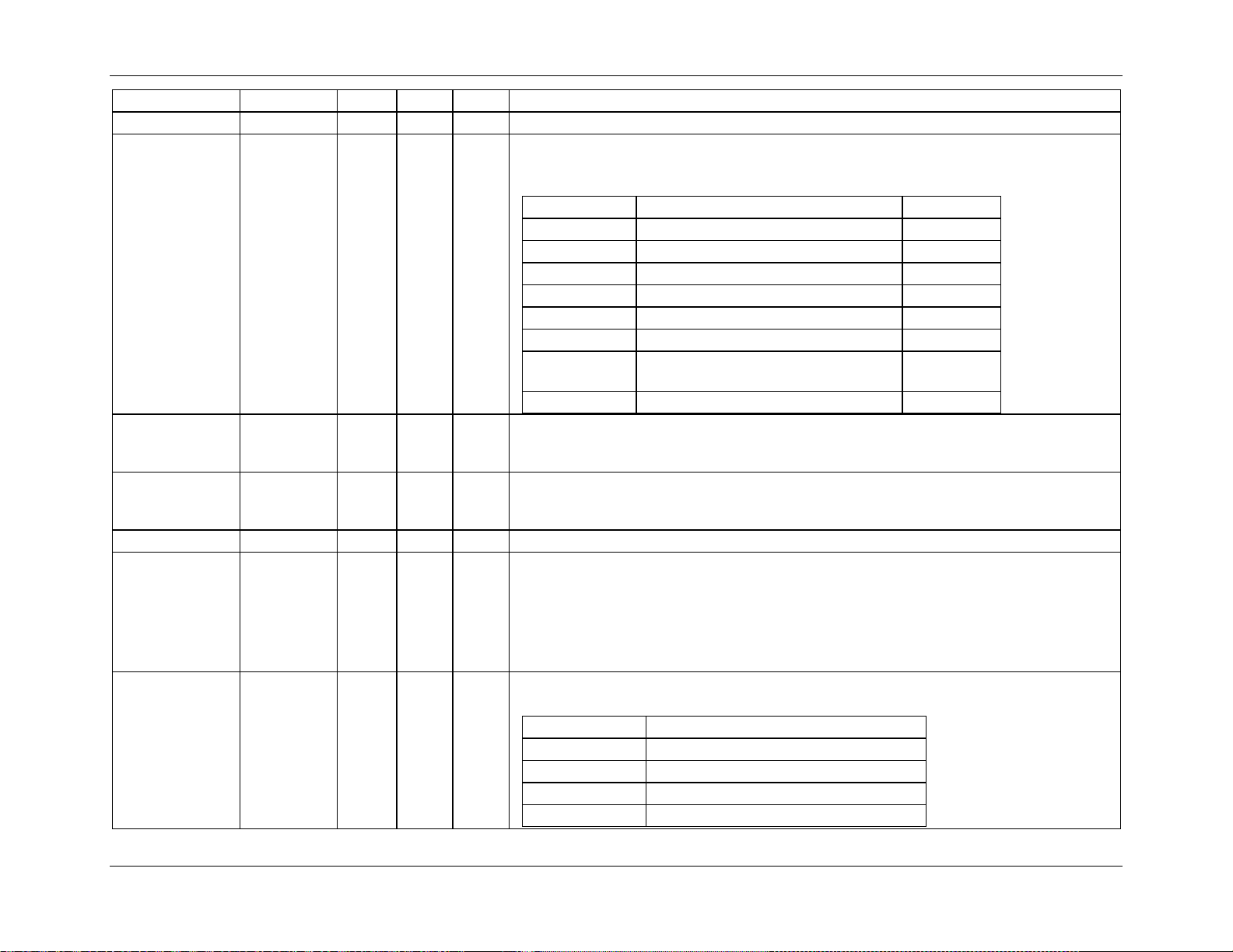
Data Sheet 71M6531D/F-71M6532D/F FDS 6531/6532 005
Name
Location
Reset
Wake
Dir
Description
Function
COMP_STAT[0]
DI_RPB[2:0]
DIO_R1[2:0]
DIO_R2[2:0]
DIO_R4[2:0]
DIO_R5[2:0]
DIO_R6[2:0]
DIO_R7[2:0]
DIO_R8[2:0]
DIO_R9[2:0]
DIO_R10[2:0]
DIO_R11[2:0]
DIO_RRX[2:0]
DIO_DIR0[7:1]
DIO_DIR1[7:0]
DIO_DIR2[1]
DIO_0[7:0]
DIO_1[7:0]
DIO_2[1]
DIO_3[5:4]
DIO_EEX[1:0]
2003[0] – – R Status bit for the V1 comparator (same as V1_OK, see TMUXOUT)
2009[2:0]
2009[6:4]
200A[2:0]
200B[2:0]
200B[6:4]
200C[2:0]
200C[6:4]
200D[2:0]
200D[6:4]
200E[2:0]
200E[6:4]
20AF[2:0]
0
0
0
0
0
0
0
0
0
0
0
0
0
0
0
0
0
0
0
0
0
0
0
0
R/W
Connects dedicated I/O pins DIO2 and DIO4 through DIO11 as well as input pins PB,
DIO1 and RX to internal resources. If more than one input is connected to the same
resource, the Multiple column in the table below specifi es how they are combined.
DIO_Rx[2:0] Resource Multiple
000 NONE –
001 Reserved OR
010 T0 (Counter /Timer 0 clock or gate) OR
011 T1 (Counter /Timer 1 clock or gate) OR
100 High priority IO interrupt (int0 rising) OR
101 Low priority IO interrupt (int1 rising) OR
110
111 Low priority IO interrupt (int1 falling) OR
High priority IO interrupt (int0 falling)
OR
Programs the direction of DIO pins 7 through 1. 1 i ndi cat es an output. The bits are
SFR A2 [7:1] 0 – R/W
ignored if the pin is not configured as DI O. See DIO_PV and DIO_PW for special options
for DIO6 and DIO7. See DIO_EEX[1:0] for special options for DIO4 and DIO5.
Programs the direction of DIO pins 15 through 8. 1 i ndi cates an output. The bits are
SFR 91 0 – R/W
ignored if the pin is not configured as I/O. See DIO_PX and DIO_PW for special options
for the DIO8 and DIO9 outputs.
SFR A1[1] 0 – R/W Programs the direction of DIO17.
The value on the DIO pins. Pins conf igure d as LCD will rea d zero. When w ritten, c hanges
SFR 80
SFR 90
SFR A0[1]
SFR B0[5:4]
0
0
0
0
−
–
–
–
R/W
R/W
R/W
R/W
data on pins configured as outputs. Pins configured as LCD or input will ignore writes.
DIO_0[7:1] corresponds to DIO7 through DIO1. PB is read on DIO_0[0].
DIO_1[7:0] corresponds to DIO15 through DIO8.
DIO_2[1] corresponds to DIO17.
DIO_3[5:4] corresponds to DIO28 and DIO29.
When set, converts DIO4 and DIO5 to interface with external EEPROM. DIO4 becomes
SDCK and DIO5 becomes bi-directional SDATA.
DIO_EEX[1:0]
2008[7:6] 0 0 R/W
00 Disable EEPROM interface
01 2-Wire EEPROM interface
10 3-Wire EEPROM interface
11 not used
78 © 2005-2010 TERIDIAN Semiconductor Corporation v1.3
Page 79
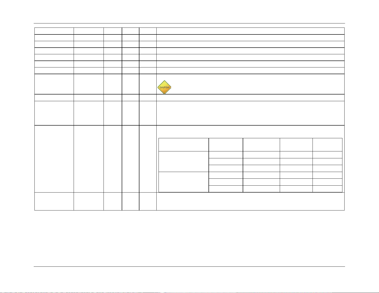
FDS 6531/6532 005 Data Sheet 71M6531D/F-71M6532D/F
Name
Location
Reset
Wake
Dir
Description
DIO_PX
200F[3]
0 0 R/W
Causes XPULSE to be output on DIO8.
200F[2]
0 0 R/W
Causes YPULSE to be output on DIO9.
EX_XFR
2002[0]
0
0
R/W
DIO_PV
DIO_PW
DIO_PY
EEDATA[7:0]
EECTRL[7:0]
ECK_DIS
EQU[2:0]
EX_RTC
EX_FWCOL
EX_PLL
FIR_LEN[1:0]
FL_BANK[2:0]
2008[2] 0 0 R/W Causes VARPULSE to be output on DIO7.
2008[3] 0 0 R/W Causes WPULSE to be output on DIO6.
SFR 9E 0 0 R/W Serial EEPROM interface data.
SFR 9F 0 0 R/W Serial EEPROM interface control.
Emulator clock disable. When ECK_DIS = 1, the emulator clo ck is disabled.
2005[5] 0 0 R/W
If ECK_DIS is set, the emulator and programming devices will be unable to
erase or program the device.
2000[7:5] 0 0 R/W Specifies the power equation to be used by the CE.
Interrupt enable bits. These bits enable the X F E R_BUSY, the RTC_1SEC, the Firm2002[1]
2007[4]
2007[5]
0
0
0
0
0
0
WareCollision (FWCOL) and PLL interrupts. Note that if one of these interrupts is to
be enabled, its corresponding MPU EX enable must also be set. See Section 1.4.9
Interrupts for details.
FIR_LEN[1:0] controls the length of the ADC decimation FIR filter and therefore controls
the time taken for each conversion.
[M40MHZ, M26MHZ] FIR_LEN[1:0]
Resulting FIR
Filter Cycles
[00], [10], or [11] 00 138 1 0.110017
2007[3:2] 1 1 R/W
01 288 2 1.000
10 384 3 2.37037
[01] 00 186 1 0.113644
01 384 2 1.000
10 588 3 3.590363
Flash bank. Memory above 32 KB is mapped to the MPU address space from 0x8000
SFR B6[2:0] 1 1 R/W
to 0xFFFF in 32 KB banks. When MPU address[15] = 1, the address in flash is
mapped to FL_BANK[2:0], MPU Address[14:0]. FL_BANK is reset by the erase cycle.
Resulting
CK32 Cycles
Resulting
DC Gain
v1.3 © 2005-2010 TERIDIAN Semiconductor Corporation 79
Page 80

Data Sheet 71M6531D/F-71M6532D/F FDS 6531/6532 005
Name
Location
Reset
Wake
Dir
Description
Flash Erase Initiate. (Default = 0x00). FLSH_ERASE is used to initiate either the Flash
Mass Erase cycle or the Flash Page Erase cycle. Specific patterns are expected for
FLSH_ERASE in order to initiate the appropriate Erase cycle.
FLSH_ERASE
[7:0]
SFR 94[7:0] 0 0 W
0x55 = Initiate Flash Page Erase cycle. Must be proceeded by a write to
0xAA = Initiate Flash Mass Erase cycle. Must be pro ceeded by a write to
Any other pattern written to FLSH_ERASE will have no effect. The erase cycle is not
completed until 0x00 is written to FLSH_ERASE.
Mass Erase Enable.
FLSH_MEEN
SFR B2[1] 0 0 W
0 = Mass Erase disabled (default).
1 = Mass Erase enabled.
Must be re-written for each new Mass Erase cycle.
Flash Page Erase Address. (Default = 0x00)
FLSH_PGADR
[5:0]
SFR B7 [7:2] 0 0 W
FLSH_PGADR[5:0] with FL_BANK[2:0], sets the Flash Page Address (page 0 t hrough
127) that will be erased during the Page Erase cy cle.
Must be re-written for each new Page Erase cycle.
Program Write Enable. This bit must be cleared by the MPU after each byte write op-
FLSH_PWE
SFR B2[0] 0 0 R/W
eration. Write operations to this bit are inhibit ed when interrupts are enabled.
0 = MOVX commands refer to XRAM Space, normal operation (defaul t).
1 = MOVX @DPTR,A moves A to Program Space (Flash) @ DPTR.
GP0
…
GP7
IE_FWCOL0
IE_FWCOL1
20C0
…
20C7
SFR E8[2]
SFR E8[3]
0
…
0
0
0
NV
…
NV
0
0
R/W
R/W
R/W
Non-volatile general-purpose registers p owered by the RTC supply. These registers
maintain their value in all power modes, but wil l be cleared on reset. The values of
GP0…GP7 will be undefined if VBAT drops below the minimum value.
Interrupt flags for Firmware Collision Inter rup t. See the Flash Memory section for
details.
PB flag. Indicates that a rising edge occurred on P B. Firmware must write a zero to
IE_PB
SFR E8[4] 0 – R/W
this bit to clear it. The bit is also cleared whe n the MPU requests SLEEP or LCD
mode. On bootup, the MPU can read this bit to determine if the part was woken with
the PB (DIO0[0]).
Indicates that the MPU was woken or interrupted (I NT4) by system power becoming
IE_PLLRISE
SFR E8[6] 0 0 R/W
available, or more precisely, by PLL_OK rising. The firmware must write a zero to this
bit to clear it.
Indicates that the MPU has entered BROWNOUT m ode because system power has
IE_PLLFALL
SFR E8[7] 0 0 R/W
become unavailable (INT4), or more precisely , because PLL_OK fell. This bit will not
be set if the part wakes into BROWNOUT mode be cause of PB or the WAKE timer.
The firmware must write a zero to this bit t o clear i t.
IEN_SPI
20B0[4] 0 – R/W SPI interrupt enable.
80 © 2005-2010 TERIDIAN Semiconductor Corporation v1.3
FLSH_PGADR[5:0] @ SFR 0xB7.
FLSH_MEEN @ SFR 0xB2 and the debug (CC) port must be enabled.
Page 81
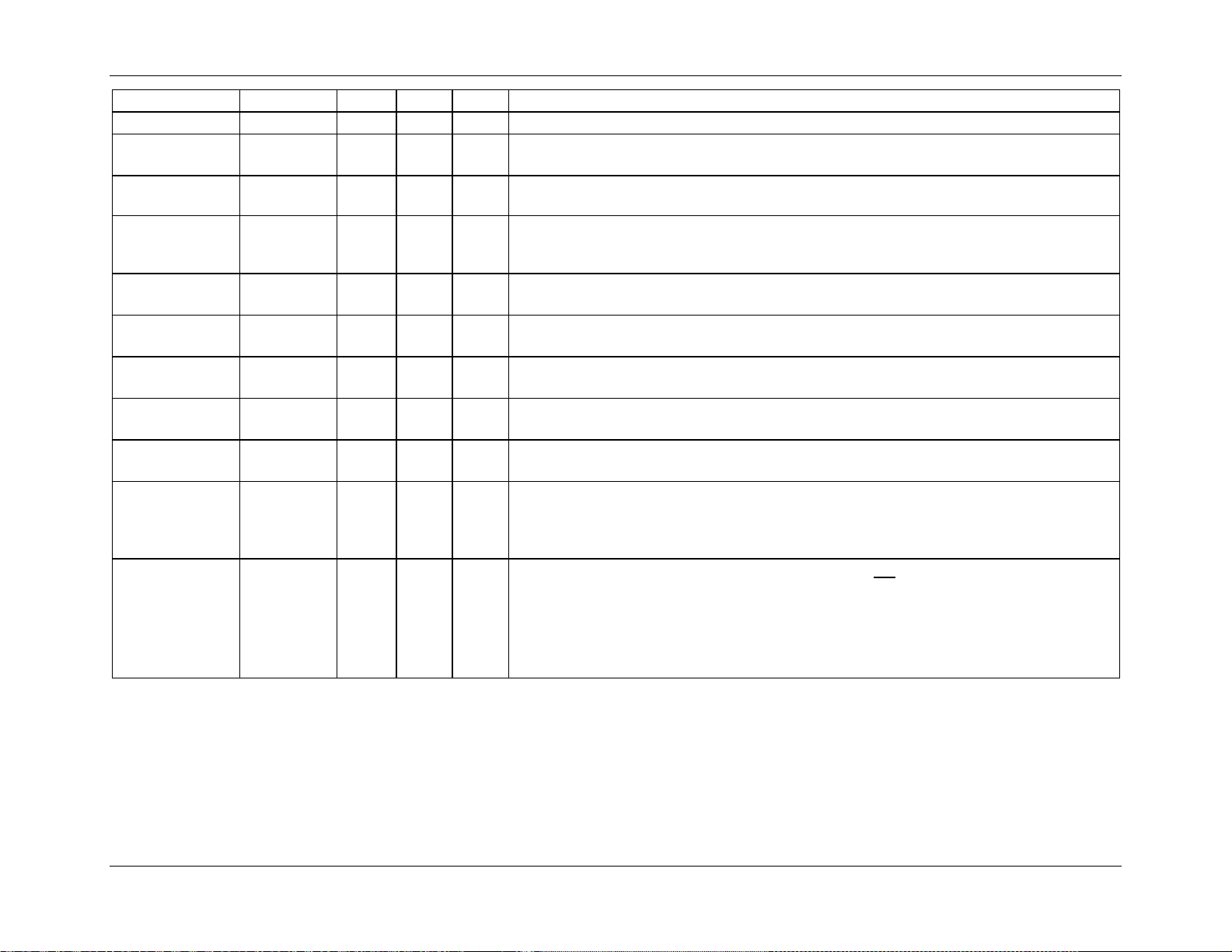
FDS 6531/6532 005 Data Sheet 71M6531D/F-71M6532D/F
Name
Location
Reset
Wake
Dir
Description
IEN_WD_NROVF
IE_XFER
IE_RTC
IE_WAKE
INTBITS
LCD_BITMAP
[31:24]
LCD_BITMAP
[39:32]
LCD_BITMAP
[55:48]
LCD_BITMAP
[63:56]
LCD_BITMAP
[71:64]
LCD_BLKMAP19
[3:0]
LCD_BLKMAP18
[3:0]
LCD_CLK[1:0]
20B0[0] 0 0 R/W Active high watchdog near overflow interrupt enable.
SFR E8[0]
SFR E8[1]
SFR E8[5] 0 – R/W
0
0
0
0
R/W
Interrupt flags. These flags monitor the XFER_BUSY interrupt and the RTC_1SEC
interrupt. The flags are set by hardware and clear automatically.
Indicates that the MPU was awakened by the autowake timer. This bit is typically read
by the MPU on bootup. The firmware must write a zero to this bit to clear it.
Interrupt inputs. The MPU may read these bits to s ee the status of external interrupts
SFR F8[6:0]
–
– R/W
INT0, INT1 up to INT6. These bits do not have any memory and are primarily intended
for debug use.
2023 0 L R/W Configuration for DIO 11/SEG 31 throug h DIO4/SE G24. Unus ed bits sho uld be set t o zero.
1 = LCD pin, 0 = DIO pin. Check Table 54 for bit availability.
2024 0 L R/W Bitmap of DIO19/SEG39 through DIO12/SEG32. Unused bit s should be s et to zero.
1 = LCD pin, 0 = DIO pin. Check Table 54 for bit availability.
2026 0 L R/W Bitmap of DIO28/SEG48 through DIO35/SEG55. U nused bit s should be set to zero.
1 = LCD pin, 0 = DIO pin. Check Table 54 for bit availability.
2027 0 L R/W Bitmap of DIO36/SEG56 through DIO43/SEG63. U nused bit s should be set to zero.
1 = LCD pin, 0 = DIO pin. Check Table 54 for bit availability.
2028 0 L R/W Bitmap of DIO44/SEG64 through DIO51/SEG71. Unused bit s should be set to zero.
1 = LCD pin, 0 = DIO pin. Check Table 54 for bit availability.
205A[7:4]
205A[3:0]
2021[1:0] 0 L R/W
0 L R/W
Identifies which segments connected to SEG18 and SEG19 should blink. 1 means
blink. The most significant bit corresponds to COM3, the least significant bit to COM0.
Sets the LCD clock frequency for COM/SEG pins (
following (f
00 = fw/2
01 = f
10 = f
11 = fw/26
= 32768 Hz):
w
9
28
w/
/27
w
not
frame rate) according to the
v1.3 © 2005-2010 TERIDIAN Semiconductor Corporation 81
Page 82
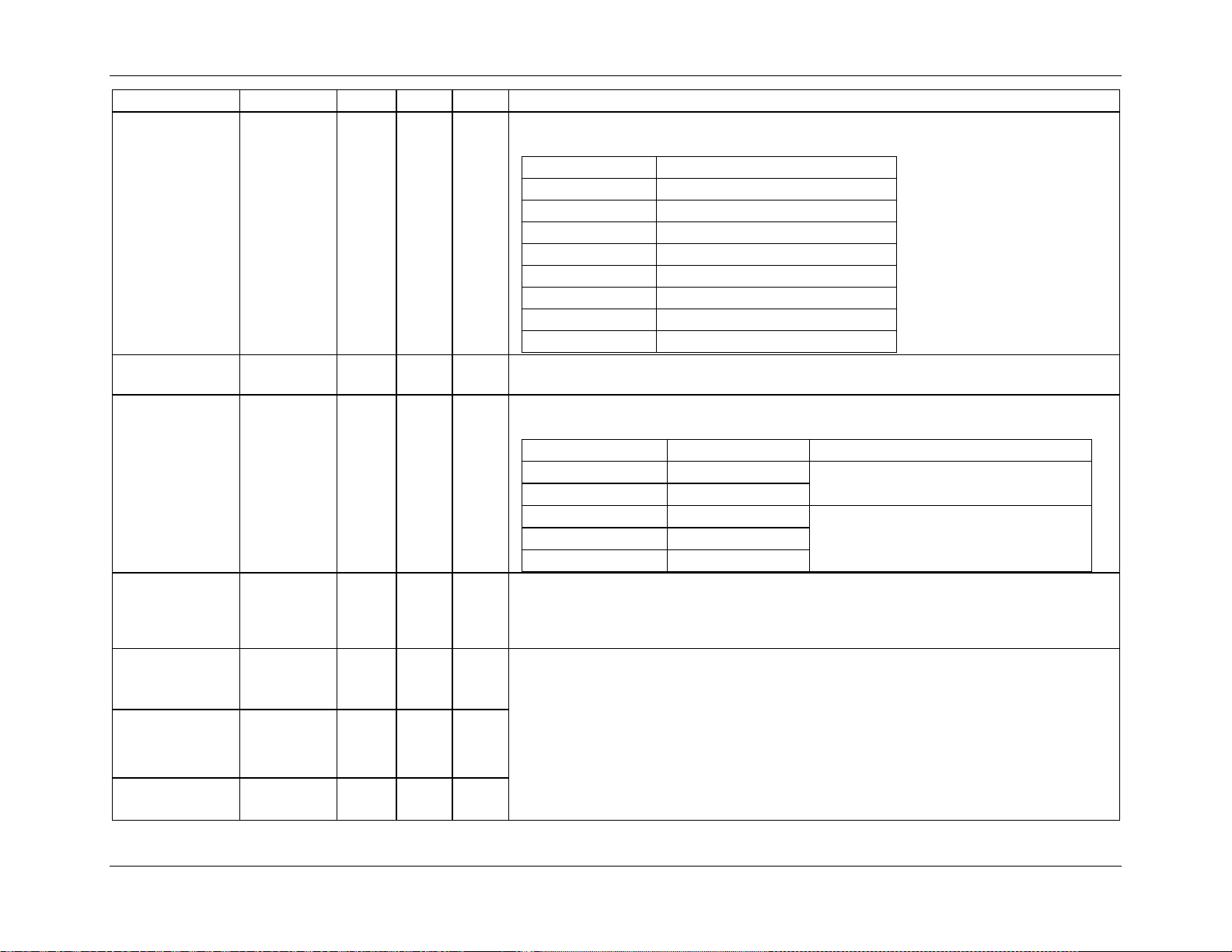
Data Sheet 71M6531D/F-71M6532D/F FDS 6531/6532 005
Name
Location
Reset
Wake
Dir
Description
LCD contrast control DAC. Adjusts the LCD voltage in steps of 0.2 V from V3P3SYS
(mission mode) or VBAT (brownout/LCD mode s).
LCD_DAC[2:0] Resulting LCD Voltage
000 V3P3 or VBAT
001 V3P3 or VBAT – 0.2V
LCD_DAC[2:0]
20AB[3:1] 0 L R/W
010 V3P3 or VBAT – 0.4V
011 V3P3 or VBAT – 0.6V
100 V3P3 or VBAT – 0.8V
101 V3P3 or VBAT – 1.0V
110 V3P3 or VBAT – 1.2V
111 V3P3 or VBAT – 1.4V
LCD_E
2021[5] 0 L R/W
Enables the LCD display. When disabled, VLC2, VLC1 and VLC0 are ground as are
the COM and SEG outputs.
The LCD bias mode. Use the LCD DAC in ANACTRL to reduce saturation. The number
of states is the number of commons which are driv en to multiplex the LCD.
LCD_MODE[2:0] Function Notes
LCD_MODE[2:0]
2021[4:2] 0 L R/W
000 4 states, ⅓ bias ⅓ bias modes can drive 3.3 V LCDs.
001 3 states, ⅓ bias
010 2 states, ½ bias
011 3 states, ½ bias
100 static display
½ bias and static modes can drive
both 3.3 V and 5 V LCDs.
Puts the part to sleep, but with the LCD display still active. LCD_ONLY is ignored if
LCD_ONLY
20A9[5] 0 0 W
system power is present. While in SLEEP mode, the device will wake up on reset,
when the autowake timer times out, when the push button is pushed, or when system
power returns.
LCD_SEG0[3:0]
…
LCD_SEG19[3:0]
LCD_SEG24[3:0]
…
LCD_SEG31[3:0]
2030[3:0]
…
2043[3:0]
2048[3:0]
…
204F[3:0]
0
…
0
0
…
0
L
…
L
L
…
L
R/W
…
R/W
R/W
…
R/W
LCD Segment Data. Each word contains inform ation for 1 to 4 time divisions of each
segment. Some addresses are used to address t wo segments.
In each word, bit 0 corresponds to COM0, bit 1 t o COM 1, bit 2 to COM2 and bit 3 to
COM3 of the first segment. Bits 4 through 7 correspond to COM0 to COM3, respec-
tively, of the second segment.
Care should be taken when writing to LCD_SEG locations since some of them control
LCD_SEG32[3:0]
2050[3:0] 0 L R/W
DIO pins.
82 © 2005-2010 TERIDIAN Semiconductor Corporation v1.3
Page 83
FDS 6531/6532 005 Data Sheet 71M6531D/F-71M6532D/F
Name
Location
Reset
Wake
Dir
Description
MPU_DIV[2:0]
Resulting Clock Frequency
000
MCK/22
011
MCK/25
100
MCK/26
111
MCK/28
LCD_SEG33[3:0]
…
LCD_SEG35[3:0]
LCD_SEG37[3:0]
LCD_SEG39[3:0]
…
LCD_SEG41[3:0]
LCD_SEG48[7:4]
…
LCD_SEG49[7:4]
LCD_SEG63[7:4]
…
LCD_SEG66[7:4]
LCD_SEG71[7:4]
…
LCD_SEG73[7:4]
LCD_Y
M26MHZ
M40MHZ
2051[3:0]
…
2053[3:0]
0
…
0
L
…
L
R/W
…
R/W
2055[3:0] 0 L R/W
2057[3:0]
…
2059[3:0]
2036[7:4]
…
2037[7:4]
2045[7:4]
…
2048[7:4]
204D[7:4]
…
204F[7:4]
0
…
0
0
…
0
0
…
0
0
…
0
L
…
L
L
…
L
L
…
L
L
…
L
R/W
…
R/W
R/W
…
R/W
R/W
…
R/W
R/W
…
R/W
2021[6] 0 L R/W
2005[4]
2005[0]
0
0
0
0
R/W
R/W
LCD Blink Frequency (ignored if blink is disabled or if the segment is off).
0 = 1 Hz (500 ms ON, 500 ms OFF)
1 = 0.5 Hz (1 s ON, 1 s OFF)
M26MHZ and M40MHZ set the master clock (MCK) frequen cy . These bits are reset on
chip reset and may only be set. Attempts to write zeroes to M40MHZ and M26MHZ.are
ignored.
The MPU clock divider (from MCK). These bits may be programmed by MPU without
risk of losing control.
MPU_DIV[2:0]
v1.3 © 2005-2010 TERIDIAN Semiconductor Corporation 83
2004[2:0] 0 0 R/W
001 MCK/23
010 MCK/24
101 MCK/27
110 MCK/28
Page 84
Data Sheet 71M6531D/F-71M6532D/F FDS 6531/6532 005
Name
Location
Reset
Wake
Dir
Description
.
The MPU asserts this bit when it wishes the M UX to perform ADC conversions on an
MUX_ALT
2005[2] 0 0 R/W
alternate set of inputs.
If CHOP_E[1:0] is 00, MUX_ALT is automatically asserted once per sumcycle, when
XFER_BUSY falls.
MUX_DIV[3:0]
MUX_SYNC_E
209D[3:0] 0 0 R/W The number of states in the input multiplexer.
2020[7] 0 0 R/W When set, SEG7 outputs MUX_SYNC. Otherwise, SEG7 i s an LCD pin.
Selects the modulation duty cycle for OPT_TX.
OPT_FDC[1:0]
2007[1:0] 0 0 R/W
OPT_FDC[1:0]
00 50% Low
Function
01 25% Low
10 12.5% Low
11 6.25% Low
OPT_RXDIS
OPT_RXINV
2008[5] 0 0 R/W
2008[4] 0 0 R/W
Configures OPT_RX to an analog input to the optical UART comparator or as a digital
input/output, DIO1: 0 = OPT_RX, 1 = DIO1.
Inverts the result from the OPT_RX comparator when 1. Affects only the UART i nput.
Has no effect when OPT_RX is used as a DIO input .
Configures the OPT_TX output pin.
OPT_TXE[1:0]
2007[7:6] 00 00 R/W
OPT_TXE[1:0]
00 OPT_TX
Function
01 DIO2
10 WPULSE
11 RPULSE
OPT_TXINV
2008[0] 0 0 R/W Inverts OPT_TX when 1. This inversion occurs before modulation.
Enables modulation of OPT_TX. When OPT_TXMOD is set, O P T _TX is modulated
OPT_TXMOD
2008[1] 0 0 R/W
when it would otherwise have been zero. The modulation is applied after any inversion
caused by OPT_TXINV.
PLL_OK
2003[6] 0 0 R Indicates that system power is present and the clock generation PLL is settled.
Determines the maximum width of the pulse (low going pulse).
PLS_MAXWIDTH
[7:0]
2080[7:0] FF FF R/W
The maximum pulse width is (2*PLS_MAXWIDTH + 1)*TI. Where TI is PLS_INTERVAL
If PLS_INTERVAL = 0, TI is the sample time (397 µs). If set to 255, pulse width control
is disabled and pulses are output with a 50% duty cycle.
PLS_INTERVAL
[7:0]
2081[7:0] 0 0 R/W
For PULSE_W and PULSE_V only: If the FIFO is used, PLS_INTERVAL must be set to
81. If PLS_INTERVAL = 0, the FIFO is not used and pulses are out put as soon as the
CE issues them.
84 © 2005-2010 TERIDIAN Semiconductor Corporation v1.3
Page 85
FDS 6531/6532 005 Data Sheet 71M6531D/F-71M6532D/F
Name
Location
Reset
Wake
Dir
Description
PREBOOT
–
–
PLS_INV
PREG[16:0]
PRE_SAMPS[1:0]
QREG[1:0]
RST_SUBSEC
RTCA_ADJ[6:0]
RTC_SEC[5:0
RTC_MIN[5:0]
RTC_HR[4:0]
RTC_DAY[2:0]
RTC_DATE[4:0]
RTC_MO[3:0]
RTC_YR[7:0]
RTM_E
RTM0[9:0]
RTM1[9:0]
RTM2[9:0]
RTM3[9:0]
2004[6] 0 0 R/W
SFRB2[7]
201C[2:0]
201D[7:0]
201E[7:2]
4
0
0
4
0
0
R/W
R/W
R/W
Inverts the polarity of the pulse outputs. Normally, these pulses are active low. When
inverted, they become active high.
R Indicates that the preboot sequence is active.
RTC adjust. See Section 1.5.3 Real-Time Clock (RTC) for additional details.
0x0FFBF ≤ PREG[16:0] ≤ 0x10040
PREG[16:0] and QREG[1:0] are separate in hardware but can be programmed with a
single number calculated by the MPU.
The duration of the pre-summer, in samples.
PRE_SAMPS[1:0] Pre-summer Duration
2001[7:6] 0 0 R/W
00 42
01 50
10 84
11 100
201E[1:0] 0 0 R/W RTC adjust. See Section 1.5.3 Real-Time Clock (RTC) for additional details.
2010[0] 0 0 R/W The sub-second counter is restarted when a 1 is written to this bit.
2011[6:0] 40 – R/W Analog RTC adjust. See Section 1.5.3 Real-Time Clock (RTC) for additional details.
These are the year, month, day, hour, minute and second parameters of the RTC.
2015
2016
2017
2018
2019
201A
201B
*
*
*
*
*
*
*
NV
NV
NV
NV
NV
NV
NV
R/W
Writing to these registers sets the time. Each write operation to one of these registers
must be preceded by a write to 0x201F (WE). Valid values for each parameter are:
SEC: 00 to 59, MIN: 00 to 59, HR: 00 to 23 (00 = Midnight)
DAY: 01 to 07 (01 = Sunday), DATE: 01 to 31, MO: 01 to 12
YR: 00 to 99 (00 and all others divisible by 4 are leap years)
Values in the RTC registers are undefined when the IC powers up without a battery but
are maintained through mission and battery modes when a sufficient voltage is maintained
at the VBAT pin.
* no change of value at reset.
2002[3] 0 0 R/W Real Time Monitor (RTM) enable. When 0, the RTM output is low.
2060[9:8]
2061[7:0]
2062[9:8]
2063[7:0]
2064[9:8]
2064[7:0]
2065[9:8]
2066[7:0]
0
0
0
0
0
0
0
0
0
0
0
0
0
0
0
0
R/W
The four RTM probes. Before each CE code pass, the values of these registers are
serially output on the RTM pin. The RTM register s are ignored when RTM_E = 0.
v1.3 © 2005-2010 TERIDIAN Semiconductor Corporation 85
Page 86
Data Sheet 71M6531D/F-71M6532D/F FDS 6531/6532 005
Name
Location
Reset
Wake
Dir
Description
initialization.
When set, enables security provisions that prevent external reading of the flash memory
SECURE
SFRB2[6] 0 – R/W
(zeros will be returned if the flash is read). SECURE should be set during t he preboot
phase, i.e. while PREBOOT is set. SECURE is cleared when the flash is mas s-erased
and when the chip is reset. The bit may only be set, attempts to write zero are ignored.
SEL_IAN
SEL_IBN
20AC[1] 0 0 R/W
20AC[5] 0 0 R/W
When set to 1, selects differential mode for the cur rent input (IAP, IAN). When 0, the
input remains single-ended (71M6532D/F onl y).
When set to 1, selects differential mode for the cur rent input (IBP, IBN). When 0, the
input remains single-ended (71M6532D/F only).
Puts the 71M6531 into SLEEP mode. This bit is ignored if system power is present.
SLEEP
20A9[6] 0 0 W
The 71M6531 will wake when the autowake timer t imes out, when the push button is
pushed, when system power returns, or when RE S ET goes high.
SLOT0_SEL[3:0]
SLOT1_SEL[3:0]
SLOT2_SEL[3:0]
SLOT3_SEL[3:0]
SLOT0_ALTSEL
[3:0]
SLOT1_ALTSEL
[3:0]
SLOT2_ALTSEL
[3:0]
SLOT3_ALTSEL
[3:0]
SP_ADDR[15:8]
SP_ADDR[7:0]
SP_CMD
SPE
2090[3:0]
2090[7:4]
2091[3:0]
2091[7:4]
2096[3:0]
2096[7:4]
2097[3:0]
2097[7:4]
0
1
2
3
A
1
2
3
0
1
2
3
R/W
Primary multiplexer frame analog input sele ct i on. These bits map the selected input,
0-3 to the multiplexer state. The ADC output is always written to the memory location
corresponding to the input, regardless of which mul tiplexer state an input is mapped to
(see Section 1.2 Analog Front End (AFE)).
A
1
B
3
R/W
Alternate multiplexer frame analog input selection. Maps the selected input to the
multiplexer state.
The additional inputs, 10 and 11 in the alternate f rame are:
10 = TEMP
11 = VBAT
2072[7:0]
2073[7:0]
0
0
0
0
R
SPI Address. 16-bit address from the bus master.
R
2071 0 0 R SPI command. 8-bit command from the bus master.
2070[7] 0 0 R/W SPI port enable. Enables the SPI interface on pins SEG3 through SEG5.
SPI interrupt flag. The flag is set by the hardware and is cleared by the firmware writing
SPI_FLAG
20B1[4] 1 1 R/W
a 0. Firmware using this interrupt should clear the spurious interrupt indication during
SUBSEC[7:0]
2014[7:0]
– –
R
SUBSEC may be read by the MPU after the one second interrupt and before reaching
the next one second boundary. Setting RST_SUBSEC will clear SUBSEC.
The remaining count, in terms of 1/256 RTC cycles, to the next one second boundary.
SUM_CYCLES
[5:0]
TMUX[4:0]
TRIM[7:0]
2001[5:0] 0 0 R/W The number of pre-summer outputs summed in the final summing stage of the CE.
20AA[4:0] 2 – R/W
Selects one of 32 signals for TMUXOUT. For detail s, see Section 1.5.17 Test Ports
(TMUXOUT pin).
20FF 0 0 R/W Contains fuse information, depending on the value written to TRIMSEL[3:0].
86 © 2005-2010 TERIDIAN Semiconductor Corporation v1.3
Page 87
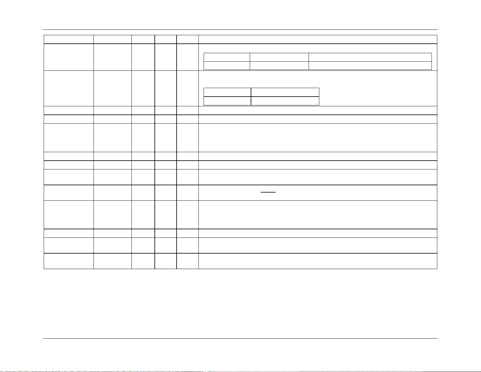
FDS 6531/6532 005 Data Sheet 71M6531D/F-71M6532D/F
Name
Location
Reset
Wake
Dir
Description
Trim Fuse
Purpose
– – –
Silicon Version
Selects the trim fuse to be read with the TRIM register:
TRIMSEL[3:0]
VERSION[7:0]
20FD[3:0] 0 0 R/W
2006
20C8
–
R
R
TRIMSEL[3:0]
1
TRIMT[7:0]
Trim for the magnitude of VREF
The device version index. This word may be read by the firmware to determine the
silicon version.
VERSION[7:0]
0001 0101 A05
VREF_CAL
VREF_DIS
2004[7] 0 0 R/W Brings VREF to the VREF pad. This feature is disabled when VREF_DIS =1.
2004[3] 0 0 R/W Disables the internal voltage reference.
Arm the autowake timer. Writing a 1 to this bit arms the autowake timer and presets it
WAKE_ARM
20A9[7] 0 – W
with the values pr ese ntl y i n WAKE_PRD and WAKE_RES. The autowake timer is reset and
disarmed whenever the IC is in MISSION or BROWNOUT mode. The timer must be
armed at least three RTC cycles before the SLEEP or LCD-ONLY mode is commanded.
WAKE_PRD
WAKE_RES
WD_NROVF_
FLAG
WD_RST
20A9[2:0] 001 – R/W Sleep time. Time = WAKE_PRD[2:0]*WAKE_RES. Default = 001. Maximum value is 7.
20A9[3] 0 – R/W Resolution of WAKE timer: 1 = 1 minute, 0 = 2.5 seconds.
20B1[0] – 0 R/W
This flag is set approximately 1 ms before the watchdog timer overflows. It is cleared
by writing a 0 or on the falling edge of WAKE.
SFR F8[7] 0 0 W
WD timer bit. This bit
this bit are: Write 0xFF: Resets the WDT.
must
be accessed with byte operations. Operations possible for
The WD overflow status bit. This bit is set when the WD timer overflows. It is powered
WD_OVF
2002[2] 0 0 R/W
by the nonvolatile supply and at bootup will indicate if the part is recovering from a WD
overflow or a power fault. This bit should be cle ared by the MPU on bootup. It is also
automatically cleared when RESET is high.
WE
WRPROT_BT
WRPROT_CE
201F[7:0] – – W
SFR B2[5] 0 0
SFR B2[4] 0 0
An 8-bit value has to be written to this address prior to accessing the RTC registers.
When set, this bit protects flash addresses from 0 to BOOT_SIZE*1024 from flash page
erase.
When set, this bit protects flash addresses from CE_LCTN*1024 to the end of memory
from flash page erase.
v1.3 © 2005-2010 TERIDIAN Semiconductor Corporation 87
Page 88

Data Sheet 71M6531D/F-71M6532D/F FDS 6531/6532 005
4.3 CE Interface Description
4.3.1 CE Progra m
The CE performs the precision computat i ons necessary to accurately measure energy. Different code
variations are used for EQU[2:0] = 0 and EQU[2:0] = 1 or 2. The computations include offset cancellation,
products, product smoothing, product summati on, frequency detection, VAR calculation, sag detection,
peak detection and voltage phase measurement. All data computed by the CE is dependent on the
selected meter equation as given by EQU[2:0]. Although EQU[2:0] = 0 and EQU[2:0] = 2 have the same
element mapping, the MPU code can use the value of EQU[2:0] to decide if element 2 is used for tamper
detection (typically done by connecting VB to VA) or as a second independent element.
The CE program is supplied by Teridian as a data image that can be merged with the MPU operational
code for meter applications. Typically, the CE pro gram covers most applications and does not need to be
modified. Other variations of CE code may be available from TERIDIAN. The description in this section
applies to CE code revision CE31A04 (for EQU[2:0] = 0). Deviations for code revision CE31A03 (for
EQU[2:0] = 1 or 2) are noted where applicable.
4.3.2 CE Data Format
All CE words are 4 bytes. Unless specified otherwise, they are in 32-bit two’s complement format
(-1 = 0xFFFFFFFF). Calibration parameters are defined in flash memory (or ext ernal EEPROM) and
must be copied to CE data memory by the MPU before enabling the CE. Internal variables are used in
internal CE calculations. Input variables allow the MP U to control the behavior of the CE code. Output
variables are outputs of the CE calculations. The c orresponding MPU address for the most si gnificant
byte is given by 0x0000 + 4 x CE_address and by 0x0003 + 4 x CE _address for the least significant byte.
4.3.3 Constants
Constants used in the CE Data Memory tables are:
• F
= 32768 Hz/13 = 2520.62 Hz.
S
• F
is the fundamental frequency.
0
• IMAX is the external rms current corresponding to 25 0 mV pk at the inputs IA and IB.
• VMAX is the external rms voltage corresponding to 250 mV pk at the VA and VB inputs.
• N
ACC, the accumulation count for energy measurements is PRE_SAMPS[1:0]*SUM_CYCLES[5:0].
• The duration of the accumulation interval f or energy measurements is
PRE_SAMPS[1:0]*SUM_CYCLES[5:0]/F
S
• ln_8 is a gain constant of the current channel, n. Its value is 8 or 1 and is controlled by In_SHUNT.
• X is a gain constant of the pulse g ener ators. Its v alue i s dete rmine d by PULSE_FAST and PULSE_SLOW.
• Voltage LSB for sag detecti on = VMAX * 7.87 98*10
-6
V.
The system constants IMAX and VMAX are used by the MPU to convert internal quantities (as used by
the CE) to external, i.e. metering quantities. Their values are determined by the off-chip scaling of the
voltage and current sensors used in an actual meter. The LSB values used in this document relate digital
quantities at the CE or MPU interface to external meter input quantities. For example, if a SAG t hreshold
of 80 V peak is desired at the meter input, the digital value that should be programmed into SAG_THR
would be 80/SAG_THR
LSB, where SAG_THRLSB is the LSB value in the description of SAG_THR.
The parameters EQU[2:0], CE_E, PRE_SAMPS[1:0] and SUM_CYCLES[5:0] essential to the function of the
CE are stored in I/O RAM (see Section 4.2 I/O RAM Description – Alphabetical Order).
4.3.4 Environment
Before starting the CE using the CE_E bit, the M P U has t o est ablish the proper environment for the CE by
implementing the following steps (for CE31A04 code):
• Load the CE data into RAM.
• Establish the equation to be applied in EQU[2:0]. The CE code has to match the selected equation.
• Establish the accumulation period and number of samples in PRE_SAMPS[1:0] = 0 (multiplier = 42) and
SUM_CYCLES[5:0] = 0x3C (60).
• Set PLS_INTERVAL[7:0] to 81.
• Select the values for FIR_LEN[1:0] = 2 and MUX_DIV[3:0] = 4.
88 © 2005-2010 TERIDIAN Semiconductor Corporation v1.3
Page 89
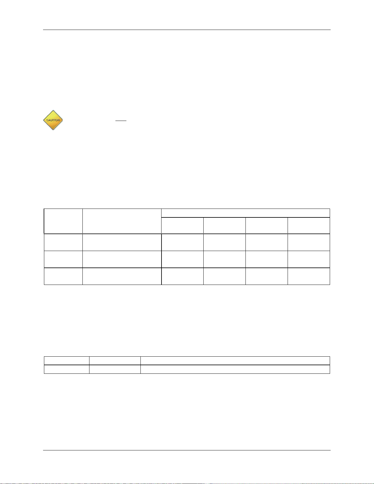
FDS 6531/6532 005 Data Sheet 71M6531D/F-71M6532D/F
Element Input Mapping
CESTATUS
CESTATUS
• Select the values for SLOT0_SEL[3:0] = 0, SLOT1_SEL[3:0] = 1, SLOT2_SEL[3:0] = 2, SLOT3_SEL[3:0]
= 3
• Select the values for SLOT0_ALTSEL[3:0] = 0x0A, SLOT1_ALTSEL[3:0] = 1, SLOT2_ALTSEL[3:0] =
0x0B, SLOT3_ALTSEL[3:0] = 3.
• Set CHOP_E[1:0] = 00.
• Initialize any MPU interrupts, such as CE_BUSY, XFER_BUSY, or a power failure detection interrupt.
When different CE codes are used, a different set of environment parameters needs to be established.
The exact values for these parameters are stated in the Application Notes and other documentation
accompanying the CE codes.
only
CE codes should
applicable CE code description. Changing environment parameters at random will lead to unpredictable results.
Typically, there are thirteen 32768 Hz cycles per ADC multiplexer frame (see Figure 19). This means that
the product of the number of cycles per frame and the number of conversions per frame must be 12 (allowing
for one settling cycle).
During operation, CHOP_E[1:0] = 00 enables the auto matic chopp ing m ode an d forces an a lterna te
multiplexer sequence at regular intervals. This enables accurate temperature measurement.
be used with environment parameters specified in this document or in the
4.3.5 CE Calculations
Table 56: CE EQU[2:0] Equations and Element Input Mapping
EQU[2:0]
0
1
2
Watt & VAR Formula
(WSUM/VARSUM)
VA IA (1 element, 2W 1
with tamper detection
VA*(IA-IB)/2
(1 element, 3W 1
VA*IA + VB*IB
(2 element, 4W 2
φ)
φ)
W0SUM/
VAR0SUM
φ)
VA*IA VA*IB IA IB
VA*(IA-IB)/2 (VA * IB)/2 IA-IB IB
VA*IA VB*IB IA IB
W1SUM/
VAR1SUM
I0SQSUM I1SQSUM
4.3.6 CE Status and Control
The CESTATUS register provides information about the status of voltage and input AC signal frequency,
which are useful for generating early power fail warnings, e.g. to initiate necessary data storage. It contains
sag warning flags for VA and VB as well as F
frequency. CESTATUS represents the status flags for the preceding CE code pass (CE busy interrupt).
Sag alarms are not remembered from one code pa ss to the next. The CE Status word is refreshed at
every CE_BUSY interrupt. The significance of the bits in CESTATUS is shown in Table 57.
CE Address Name Description
0x80
Since the CE_BUSY interrupt typically occurs at 2520.6 Hz, it is desirable to minimize the computation
required in the interrupt handler of the MPU. Rather than reading the CE status word at every CE_BUSY
interrupt and interpret the sag bits, it is recommended that the MPU activate the YPULSE output to generate
interrupts when a sag occurs (see the description of the CECONFIG register)
See description of
, the derived clock operating at the fundamental input
0
bits in Table 57.
v1.3 © 2005-2010 TERIDIAN Semiconductor Corporation 89
Page 90
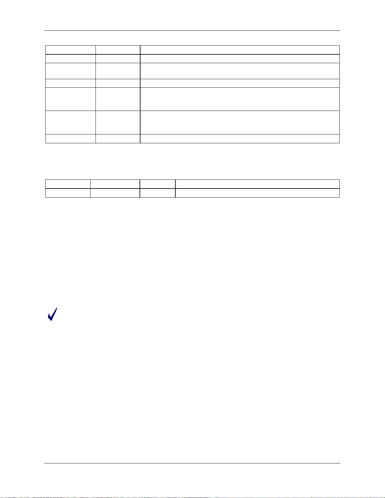
Data Sheet 71M6531D/F-71M6532D/F FDS 6531/6532 005
31:29
Not Used
These unused bits will always be zero.
SAG_THR.
CE Address
Name
Data
Description
Table 57: CESTATUS (CE RAM 0x80) Bit Definitions
CESTATUS [bit]
Name Description
28
F0
F0 is a square wave at the exact fundamental frequency for the
phase selected with the FREQSELn bits in CECONFIG.
27 Reserved
Normally zero. Becomes one when VB remains below SAG_THR for
26
SAG_B
SAG_CNT samples. Will not return to zero until VB rises above
Normally zero. Becomes one when VA remains below SAG_THR for
25
SAG_A
SAG_CNT samples. Will not return to zero until VA rises above
SAG_THR.
24:0 Not Used These unused bits will always be zero.
The CE is initialized and its functions are controlled by the MPU using CECONFIG. This register contains
in packed form SAG_CNT, FREQSEL, EXT_PULSE, I0_SHUNT, I1_SHUNT, PULSE_SLOW and PULSE_FAST.
The CECONFIG bit definitions are given in Table 58.
0x20
CECONFIG
0x5020 See description of the CECONFIG bits in Table 58.
IA_SHUNT and/or IB_SHUNT can configure their respective current inputs to accept shunt resistor sensors.
In this case the CE provides an additional gain of 8 to the selected current input. WRATE may need to be
adjusted based on the values of IA_SHUNT and IB_SHUNT. Whenever IA_SHUNT or IB_SHUNT are set to
1, In_8 (in the equation for Kh) is assigned a value of 8.
The CE pulse generator can be controlled by either the MPU (external) or CE (internal) variables. Cont rol
is by the MPU if EXT_PULSE = 1. In this case, the MPU controls the pulse rate by placing values into
APULSEW, APULSER, APULSE2 and APULSE3. By setting EXT_PULSE = 0, the CE controls the pulse rate
based on W0SUM_X and VAR0SUM_X (EQU[2:0] = 0) or WSUM_X (EQU[2:0] = 2).
If EXT_PULSE = 0 and EQU[2:0] = 2, the pulse inputs are W0SUM_X + W1SUM_X and VAR0SUM_X +
VAR1SUM_X. In this case, creep cannot be controlled since creep is an MP U f unction.
If EXT_PULSE = 0 and EQU[2:0] = 0, the pulse inputs are W0SUM_X if I0SQSUM_X > I1SQSUM_X and
W1SUM_X, if I1SQSUM_X > I0SQSUM_X.
The 71M6531 Demo Code creep function halts both internal and external pulse generation.
The EXT_TEMP bit controls the temperature com pensation mode:
• When EXT_TEMP = 0 (internal c ompens ation), the CE will cont rol the gai n using GAIN_ADJ (see Table 60)
based on PPMC, PPMC2 and TEMP_X, the difference between die temperature and the reference /
calibration temperature TEMP_NOM. Since PPMC and PPMC2 reflect the typical behavior of the
reference voltage over temperature, the internal temperature compensation eliminates the effects of
temperature-related errors of VREF only.
• When EXT_TEMP = 1 (external compensation), the MPU is allowed to control the CE gain using
GAIN_ADJ, based on any algorithm imp l em ented in MPU code.
The FREQSEL1 and FREQSEL0 bits select the phase used to control the CE-internal PLL. CE accuracy
depends on the channel selected by the FREQSEL1 and FREQSEL0 bits receiving a clean voltage signal.
90 © 2005-2010 TERIDIAN Semiconductor Corporation v1.3
Page 91
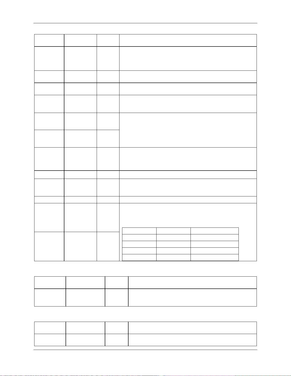
FDS 6531/6532 005 Data Sheet 71M6531D/F-71M6532D/F
Table 58: CECONFIG Bit Definitions
CECONFG
[bit]
[19]
[18]
Name Default Description
SAG_MASK1
SAG_MASK0
0
0
Sets the sag control of phase B.
Sets the sag control of phase A.
If more than one sag mask is set, a sag interrupt will onl y be
generated when all phases enabled for the inter rupt sag.
[17]
[16]
[15:8]
SAG_INT
EXT_TEMP
SAG_CNT
0
0
80
(0x50)
When set, enables the sag interrupt to be output on the
YPULSE/DIO9 pin.
When set, enables the control of GAIN_ADJ by the MPU.
When 0, enables the control of GAIN_ADJ by the CE.
The number of consecutive voltage samples belo w SAG_THR
before a sag alarm is declared. The maximum v al ue is 255.
SAG_THR is at address 0x24.
The combination of FREQSEL1 and FREQSEL0 selects the phase
[7]
FREQSEL1
0
to be used for the frequency monitor, the phase-to-phase lag
calculation, the zero-crossing counter MAINEDGE_X and the
F0 bit (CESTATUS[28]).
[6]
FREQSEL0
0
FREQSEL1/FREQSEL0 = 0/0: Phase A
FREQSEL1/FREQSEL0 = 0/1: Phase B
When zero, causes the pulse generators to respond to internal
[5]
EXT_PULSE
1
data (PULSE0 = WSUM_X, PULSE1 = VARSUM_X., PULSE2 =
VASUM_X). Otherwise, the generators respond to values the
MPU places in APULSEW and APULSER.
[4] – 0 Unused.
Address
Address
[3]
[2]
[1]
[0]
CE
0x24
CE
0x40
When 1, the current gain of channel B is increased by 8. The
IB_SHUNT
0
gain factor controlled by In_SHUNT is referred to as In_8
throughout this document.
IA_SHUNT
0 When 1, the current gain of channel A is increased by 8.
When PULSE_FAST = 1, the puls e generator input is increased
16x. When PULSE_SLOW = 1, the pulse generator input is
PULSE_FAST
0
reduced by a factor of 64. These two bits control the pulse
gain factor X (see table below). Default is 0 for both (X = 6).
PULSE_SLOW PULSE_FAST X
0 0 1.5 * 22 = 6
PULSE_SLOW
0
0 1 1.5 * 26 = 96
1 0 1.5 * 2-4 = 0.09375
1 1 Do not use
Table 59: Sag Threshold Control
Name Default Description
The threshold for sag warnings. The default value is
SAG_THR
443000
equivalent to 80 V RMS if VMAX = 600 V. The LSB val ue
is VMAX * 4.255*10
-7
V (peak).
Table 60: Gain Adjust Control
Name Default Description
GAIN_ADJ
16384
This register scales all voltage and current cha nnels. The
default value is equivalent unity gain (1.000).
v1.3 © 2005-2010 TERIDIAN Semiconductor Corporation 91
Page 92
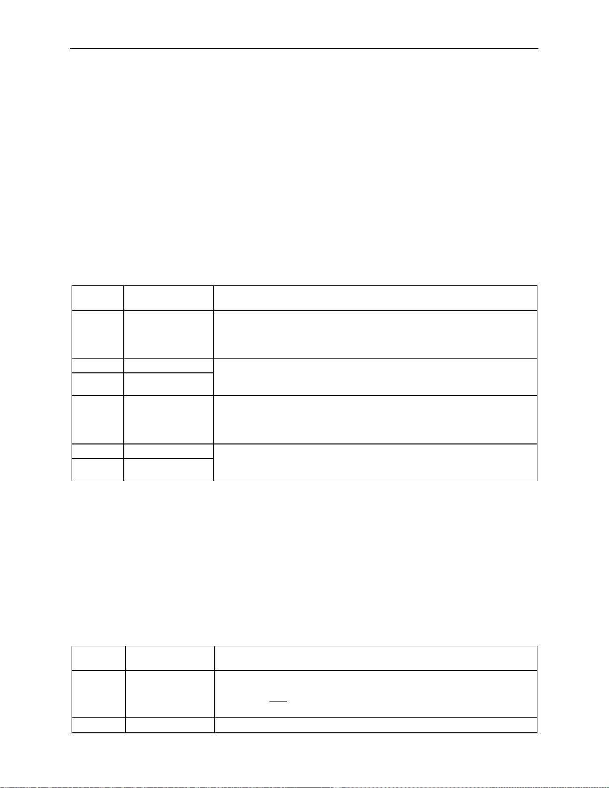
Data Sheet 71M6531D/F-71M6532D/F FDS 6531/6532 005
Address
W0SUM_X
The sum of Wh samples from each wattmet er el em ent (In_8 is the gain
VAR0SUM_X
The sum of VARh samples from each element (In_8 is the gain 1 or 8
6
32
10587.0
2
−
⋅≈≡
S
F
4.3.7 CE Transfer Variables
When the MPU receives the XFER_BUSY interrupt, it knows that fresh data is available in the transfer
variables. CE transfer variables are modified during the CE co de pass that ends with an XFER_BUSY
interrupt. They remain constant throughout each accumulation interval. In this data she et, the names of
CE transfer variables always end with _X.
The transfer variables can be categorized as:
1. Fundamental energy measurement variables
2. Instantaneous (RMS) values
3. Other measurement parameters
Fundamental Energy Measurement Variables
Table 61 describes each transfer variable for fundamental energy measurement. All variabl es are signed
32-bit integers. Accumulated variables such as WSUM are internally scaled so they have at l east 2x
margin before overflow when the integration time is one second. Additionally, the hardware will not permit
output values to fold back upon overflow.
Table 61: CE Transfer Variables
CE
0x85
0x86
0x87
0x8A
0x8B
0x8C
Name Description
For EQU[2:0] = 2, this register holds the calculated sum of Wh samples
WSUM_X
W1SUM_X
from each wattmeter element (In_8 is the gain of 1 or 8 configured by
IA_SHUNT or IB_SHUNT).
LSB = 6.6952*10
of 1 or 8 configured by IA_SHUNT or IB_SHUNT).
LSB = 6.6952*10
-13
VMAX IMAX / In_8 Wh.
-13
VMAX IMAX / In_8 Wh.
For EQU[2:0] = 2, this register holds the calculated sum of VARh
VARSUM_X
VAR1SUM_X
samples from each element (In_8 is the gain of 1 or 8 configured by
IA_SHUNT or IB_SHUNT).
LSB = 6.6952*10
configured by IA_SHUNT or IB_SHUNT).
LSB = 6.6952*10
-13
VMAX IMAX / In_8 VARh.
-13
VMAX IMAX / In_8 VARh.
WxSUM_X is the Wh value accumulated for element X in the last accumulation interval and can be computed
based on the specified LSB value.
For example, with VMAX = 600 V and IMAX = 208 A, the LSB for WxSUM_X is 0.08356 µWh.
Instantaneous Measurement Variabl es
Table 62 contains various measurement results. The Frequency measurement is computed for the phase
selected with FREQSELn bits in the CECONFIG register.
IxSQSUM_X and VxSQSUM are the squared cu rrent and vo ltage sa mples acquired during the last accumulation
interval. They can be used to calculate RMS voltages and currents. INSQSUM_X can be used for computing
the neutral current.
Table 62: CE Energy Measurement Variables
CE
Address
Name Description
Fundamental frequency.
0x82
0x8F
FREQ_X
I0SQSUM_X
LSB
The sum of squared current samples from each element.
92 © 2005-2010 TERIDIAN Semiconductor Corporation v1.3
Hz
Page 93
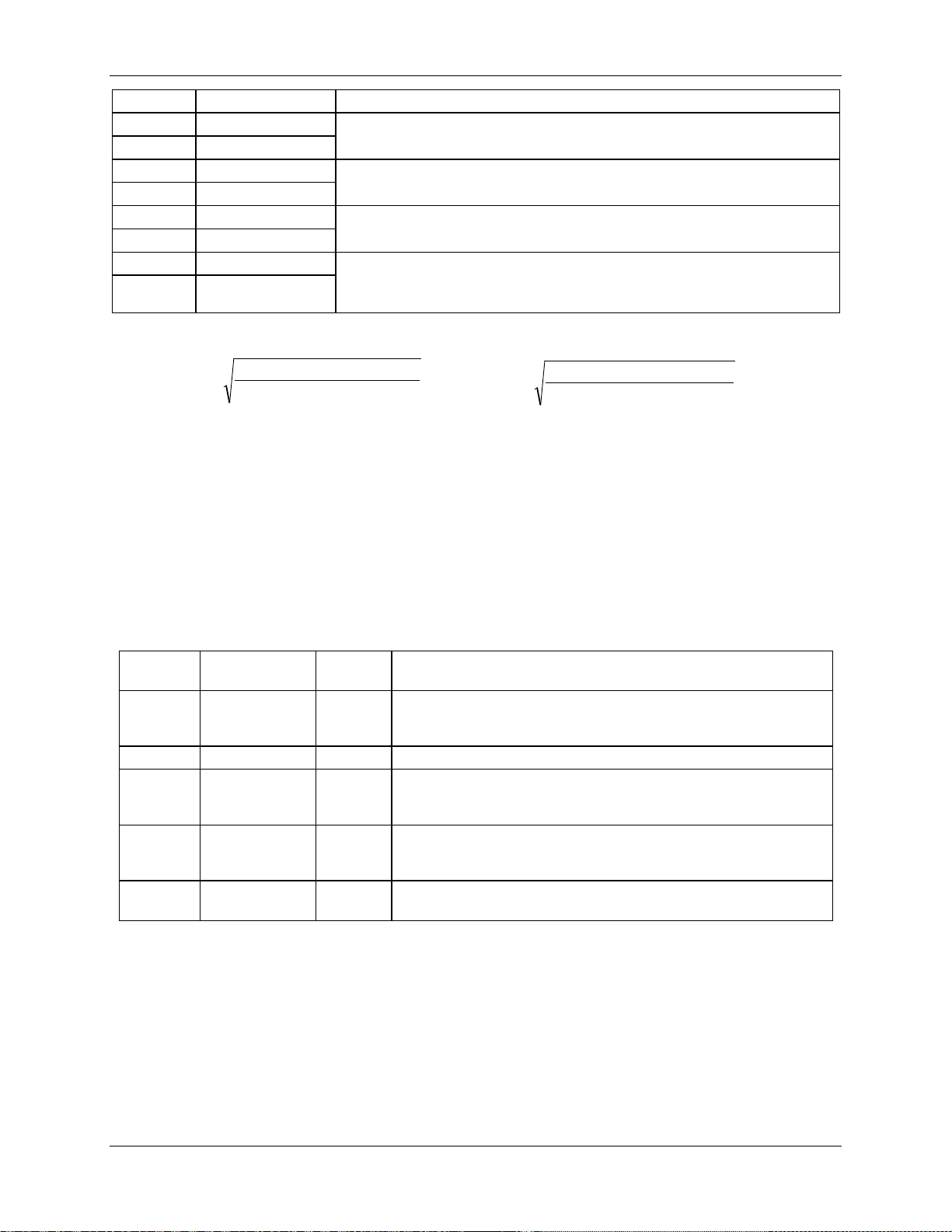
FDS 6531/6532 005 Data Sheet 71M6531D/F-71M6532D/F
LSBI = 6.6952*10
-13
IMAX2 / In_82 A2h
ACC
SI
RMS
N
FLSBIxSQSUM
Ix
⋅⋅⋅
=
3600
Address
This register contains the difference between the die tem perat ure
Scales all voltage an d curr ent i nputs. A v alue of 163 84 provide s
ACC
SV
RMS
N
FLSBVxSQSUM
Vx
⋅⋅⋅
=
3600
0x90
0x93
0x94
0x45
0x46
0x47
0x48
0x99
0x9A
I1SQSUM_X
V0SQSUM_X
V1SQSUM_X
WSUM_ACCUM
VSUM_ACCUM
SUM3_ACCUM
SUM4_ACCUM
I0SQRES_X
I1SQRES_X
The sum of squared voltage samples from each element.
LSB
= 6.6952*10
V
-13
VMAX2 V2h
These registers contain roll-over accumulators for WPULSE and
VPULSE respectively.
These registers contain roll-over accumulators for pulse outputs
XPULSE and YPULSE respectively.
These registers hold residual current measurements with doubleprecision accuracy. The exact current ISQn is:
ISQn = InSQSUM_X + 2
32
* InSQRES_X
The RMS values can be computed by the MPU from the squared current and voltage samples as follows:
Other Measurement Parameters
Table 63 describes the CE measurement parameters listed below:
• MAINEDGE_X: Useful for implementing a real-time clock based on the input AC signal. MAINEDGE_X
is the number of half-cycles accounted for in the last accumulated interval for the AC signal.
• TEMP_RAW: May be used by the MPU to monitor the chip temperature or to implement temperature
compensation.
• GAIN_ADJ: A scaling factor for measurements based on the temperature. GAIN_ADJ can be controlled
by the MPU for temperature compensati on.
• VBAT_SUM_X: This result can be used to calculate the measured battery voltage (VBAT).
Table 63: Useful CE Measurement Parameters
CE
Name Default Description
The number of zero crossings of the voltage selected with
0x83
MAINEDGE_X
N/A
FREQSELn in the previous accumulation interval. Zero crossings
are either direction and are debounced.
0x81
0x9D
TEMP_RAW_X
TEMP_X
N/A
N/A
The filtered, un-scaled reading from the temperature sensor.
and the reference/calibration temperature as established in the
TEMP_NOM register, measured in 0.1°C.
0x40
GAIN_ADJ
16384
unity gain. This register is used by the CE or by the MPU to
implement temperature compensation.
0x84
VBAT_SUM_X
N/A
Output of the battery measurement. This val ue is equivalent to
twice the measured ADC value.
4.3.8 Pulse Generation
Table 64 describes the CE pulse generation parameters WRATE, APULSEW, APULSER, APULSE2 and
APULSE3.
WRATE controls t he number of pulses that are generated per measured Wh and VARh quantities. The lower
WRATE is the slower the pulse rate for measured energy quantity. The metering constant Kh is derived from
WRATE as the amount of energy measured for each p ul se. That is, if Kh = 1 Wh/pulse, a power applied
to the meter of 120 V and 30 A (3,600 W) results in one pulse per second. If the load is 240 V at 150 A
(36,000 W), ten pulses per second will be generat ed.
The maximum pulse rate is 7.5 kHz for APULSEW and APULSER and 1.2 kHz for APULSE2 and APULSE3.
v1.3 © 2005-2010 TERIDIAN Semiconductor Corporation 93
Page 94
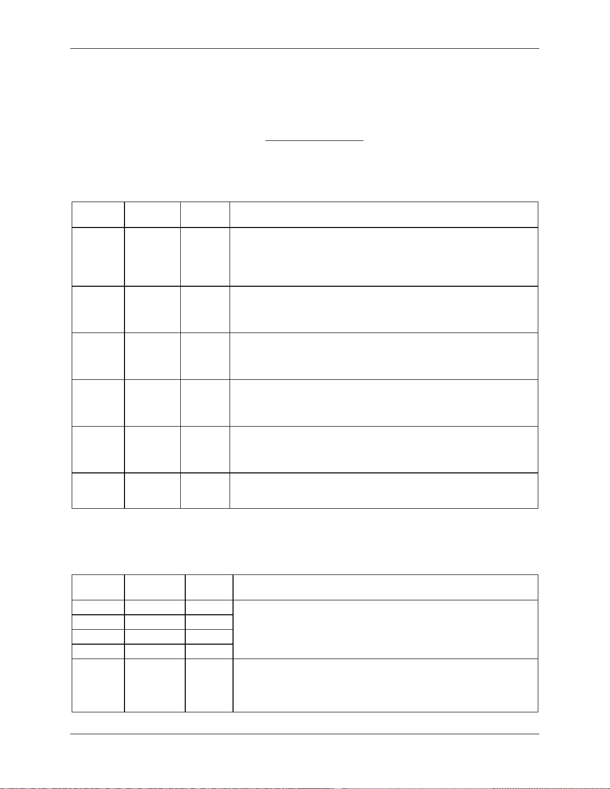
Data Sheet 71M6531D/F-71M6532D/F FDS 6531/6532 005
Hz
XFWSUMWRATE
RATE
S
46
2
⋅⋅⋅
=
take effect at the beginning of the next interval.
These constants control the gain of their respecti ve channels. The
These two constants control the CT phase com pensa tion. No
The maximum time jitter is 6 7 µs and is indep endent of t he number of pulses me asured. Thus, if the pul se
generator is monitor ed for one s econd, the peak jit ter i s 67 p pm. Aft er 10 sec onds, t he p eak jitt er i s 6.7 p pm.
The average jitter is always zero. If it is attem pted to drive either pulse generator faster than its maximum
rate, it will simply output at its maximum rate without exhibiting any rollover characteristics. The actual
pulse rate, using WSUM as an example, is:
,
where F
= sampling frequency (2520.6 Hz) and X = Pulse s peed factor (as defined in the CECONFIG
S
register with the PULSE_FAST and PULSE_SLOW bits).
Table 64: CE Pulse Generation Parameters
CE
Address
Name Default Description
Kh = VMAX*IMAX*47.1132 / (In_8*WRATE*N
default value results in a Kh of 1.0 Wh/pulse when 2520 samples
0x21
WRATE
827
are taken in each accumulation interval (and VMAX=600,
IMAX = 442 [for 400µΩ shunt], In_8 = 1, X = 6).
Maximum value = 2
Watt pulse generator input (see DIO_PW bit). The output pulse
0x41
APULSEW
0
rate is: APULSEW * F
and can be loaded during a computation interval. The change will
VAR pulse generator input (see DIO_PV bit). The output pulse rate
0x42
APULSER
0
is: APULSER * F
can be loaded during a computation interval. The ch ange will take
effect at the beginning of the next interval.
Third pulse generator input (see DIO_PV bit). The output pulse
0x43
APULSE2
0
rate is: APULSE2 * F
and can be loaded during a computation interval. The change will
take effect at the beginning of the next interval.
Fourth pulse generator input (see DIO_PV bit). The output pulse
0x44
APULSE3
0
rate is: APULSE3 * F
and can be loaded during a computation interval. The change will
take effect at the beginning of the next interval.
Register for pulse width control of XPULSE and YPULSE. The maximum pulse width is (2*PULSEWIDTH+1)*(1/FS). The default value
will generate pulses of 10 ms width at FS = 2520.62 Hz.
0x38
PULSE
WIDTH
12
15
-1.
* 2
S
-32
*2
* WRATE * X * 2
S
-32
*2
S
-32
*2
S
-32
* WRATE * X * 2
* WRATE * X * 2
* WRATE * X * 2
*X) Wh/pulse. The
ACC
-14
. This input is buffered
-14
. This input is buffered and
-14
. This input is buffered
-14
. This input is buffered
4.3.9 CE Calibration Parameters
Table 65 lists the parameters that are typically entered to effect calibration of meter accuracy.
Table 65: CE Calibration Parameters
CE
Address
0x10
0x11
0x12
0x13
0x18
94 © 2005-2010 TERIDIAN Semiconductor Corporation v1.3
Name Default Description
CAL_IA
CAL_VA
CAL_IB
CAL_VB
16384
16384
16384
16384
nominal value for each parameter is 2
channel is directly proportional to its gain constant. Thus, if the
gain of the IA channel is 1% slow, CAL_IA should be scaled by
1/(1 – 0.01) and the resulting value is 16549.
compensation occurs when PHADJ_X = 0. As PHADJ_X is increased,
PHADJ_A
0
more compensation (lag) is introduced. Range: ± 2
desired to delay the current by the angle Φ, the equations are:
14
= 16384. The gain of each
15
– 1. If it is
Page 95
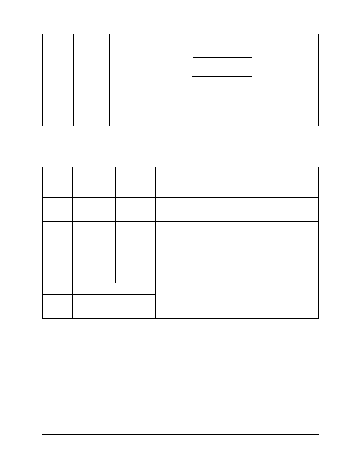
FDS 6531/6532 005 Data Sheet 71M6531D/F-71M6532D/F
Φ⋅−
Φ⋅
=
TAN
TAN
XPHADJ
0131.01487.0
02229.0
2_
20
Φ⋅−
Φ⋅
=
TAN
TAN
XPHADJ
009695.01241.0
0155.0
2_
20
This register contains the reference point for the temperature
The scale factor for the temperature calculation. It is not necessary
CE
Address
Name Default Description
at 60Hz
0x19
PHADJ_B
0
at 50Hz
0x1F
TEMP_NOM
measurement. At calibration temperature, the value read at
0
TEMP_RAW_X should be written t o TEMP_NOM. The CE will calculate
the chip temperature TEMP_X relative to the reference temperature.
0x39
DEGSCALE
9174
to use values other than the default value.
4.3.10 Other CE Parameters
Table 66 shows the CE parameters use d for suppression of noise due to scaling and truncati on effects.
The table also includes the parameter which indi cates the CE Code version.
Table 66: CE Parameters for Noise Suppression and Code Versi on
CE Ad-
dress
0x22
0x26
0x27
0x2A
0x2B
0x2E
0x2F
0x35 0x63653331
0x36 0x61303463
0x37 0x00000000
Name Default Description
KVAR
QUANT_A
6448
0
This is the scale factor for the VAR calculati on. No value
other than the default value should be applied.
These parameters are added to the Watt calcul ation for
element 0 and 1 to c ompen sate f or input noise and tr uncation.
QUANT_B
QUANT_VARA
0
0
LSB = (VMAX*IMAX / In_8) *7.4162*10
These parameters are added to the VAR calcul ation for
element A and B to compe nsate f or inp ut no ise and tru ncatio n.
QUANT_VARB
0
LSB = (VMAX*IMAX / In_8) * 7.4162*10
These parameters are added to compensate for input noise
QUANT_IA
QUANT_IB
0
0
and truncation in their respective channels in the squaring
calculations for I
LSB = VMAX
LSB = (IMAX
2
and V2.
2
*7.4162*10
2
/In_82)*7.4162*10
Text strings holding the CE version informati on as supplied
by the CE data associated with the CE code. For example,
the words 0x63653331 and 0x61303463 form the text string
“ce31a04c”.
These locations are overwritten in operation.
-10 V2
and
-10 A2
-10
W
-10
W
4.3.11 CE Flow Diagrams
Figure 41 through Figure 43 show the data fl ow through the CE in simplified form. Functions not shown
include delay compensation, sample interpol ation, scaling and processing of meter equations.
v1.3 © 2005-2010 TERIDIAN Semiconductor Corporation 95
Page 96
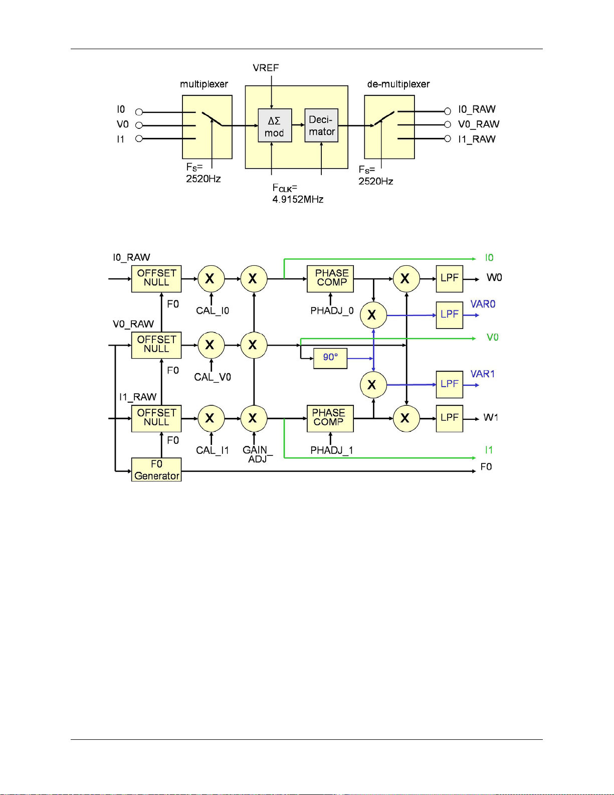
Data Sheet 71M6531D/F-71M6532D/F FDS 6531/6532 005
Figure 41: CE Data Flow: Multiplexer and ADC
Figure 42: CE Data Flow: Scaling, Gain Control, Intermediate Variables
96 © 2005-2010 TERIDIAN Semiconductor Corporation v1.3
Page 97
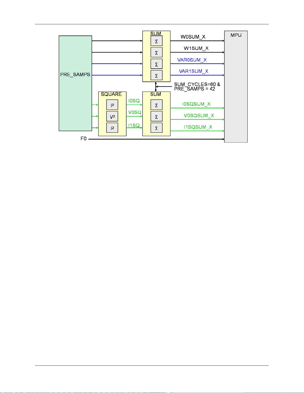
FDS 6531/6532 005 Data Sheet 71M6531D/F-71M6532D/F
Figure 43: CE Data Flow: Squaring and Summ ation S tages
v1.3 © 2005-2010 TERIDIAN Semiconductor Corporation 97
Page 98

Data Sheet 71M6531D/F-71M6532D/F FDS 6531/6532 005
Voltage and Current
Supplies and Ground Pins
Analog Input Pins
Temperature and ESD Stress
5 Electrical Specifications
5.1 Absolute Maximum Ratings
Table 67 shows the absolute maximum ranges for the device. Stresses beyond Absolute Maximum Ratings
may cause permanent damage to the device. These are stress ratings only and functional operati on at
these or any other conditions beyond those indic ated under recommended operating conditio ns (Section
5.3) is not implied. Exposure to absolute-maximum-rated conditions for extended periods may affect device
reliability. All voltages are with respect to GNDA.
Table 67: Absolute Maximum Ratin gs
V3P3SYS, V3P3A
VBAT -0.5 V to 4.6 V
GNDD -0.5 V to +0.5 V
Analog Output Pins
V3P3D
VREF
V2P5
IA, VA, IB, VB, V1
XIN, XOUT
All Other Pins
Configured as SEG or COM drivers
Configured as Digital Inputs
Configured as Digital Outputs
All other pins
−0.5 V to 4.6 V
-10 mA to 10 mA,
-0.5 V to 4.6 V
-10 mA to +10 mA,
-0.5 V to V3P3A+0.5 V
-10 mA to +10 mA,
-0.5 V to 3.0 V
-10 mA to +10 mA
-0.5 V to V3P3A+0.5 V
-10 mA to +10 mA
-0.5 V to 3.0 V
-1 mA to +1 mA,
-0.5 to V3P3D+0.5
-10 mA to +10 mA,
-0.5 to 6 V
-15 mA to +15 mA,
-0.5 V to V3P3D+0.5 V
−0.5 V to V3P3D+0.5 V
Operating junction temperature (peak, 100ms) 140 °C
Operating junction temperature (continuous) 125 °C
Storage temperature
Solder temperature – 10 second duration 250 °C
ESD stress on all pins 4 kV
98 © 2005-2010 TERIDIAN Semiconductor Corporation v1.3
−45 °C to +165 °C
Page 99
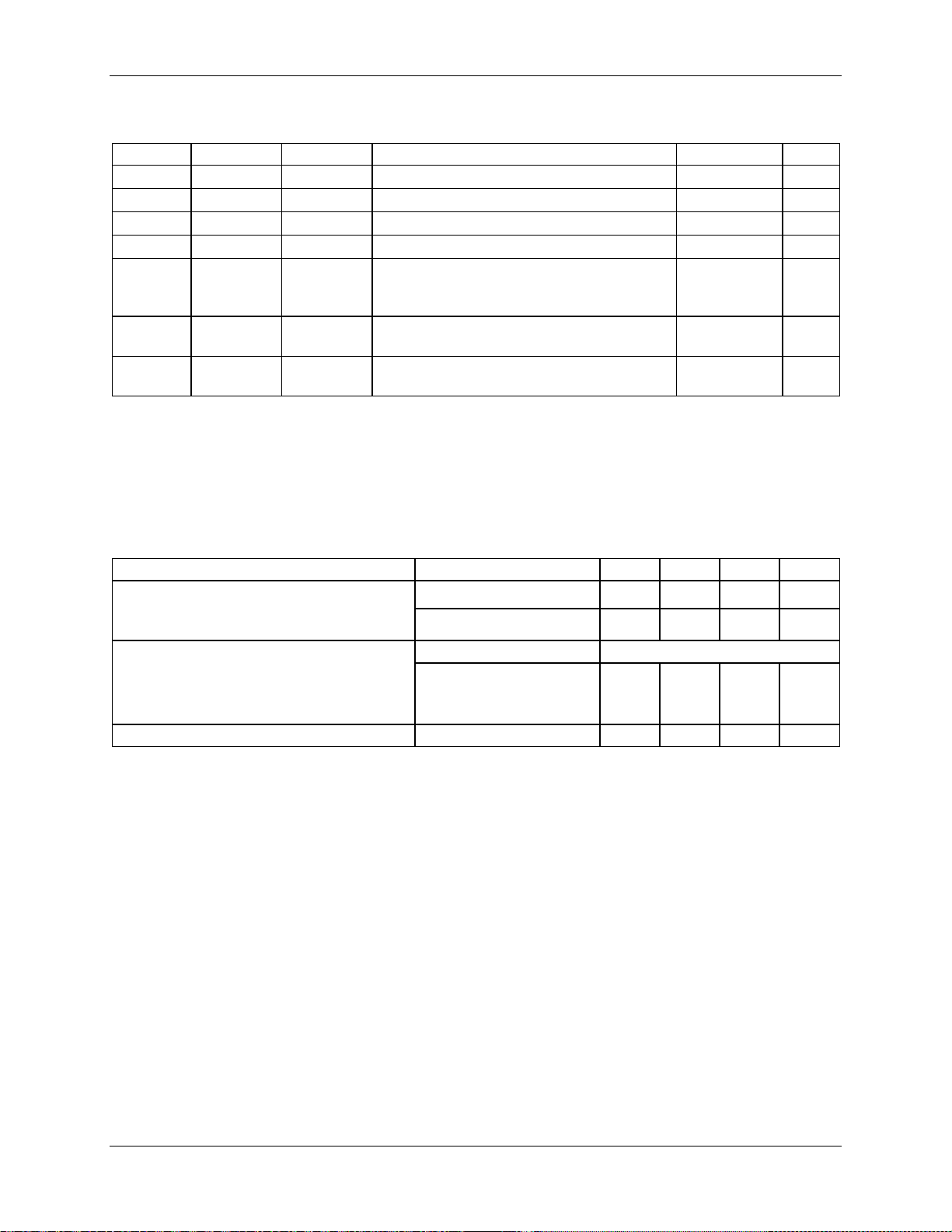
FDS 6531/6532 005 Data Sheet 71M6531D/F-71M6532D/F
Name
From
Parameter
Condition
Min
Typ
Max
Unit
5.2 Recommended External Components
Table 68: Recommended External Components
To Function Value Unit
C1 V3P3A AGND Bypass capacitor for 3.3 V supply
C2 V3P3D GNDD Bypass capacitor for 3.3 V output
CSYS V3P3SYS GNDD Bypass capacitor for V3P3SYS
C2P5 V2P5 GNDD Bypass capacitor for V2P5
≥0.1 ±20%
≥0.1 ±20%
≥1.0 ±30% µF
0.1 ±20% µF
†
µF
†
µF
32.768 kHz crystal – electrically similar to
XTAL XIN XOUT
ECS .327-12.5-17X or Vishay XT26T,
32.768 kHz
load capacitance 12.5 pF
CXS XIN AGND
CXL XOUT AGND
Load capacitor for crystal (depends on
crystal specs and board parasitics).
Load capacitor for crystal (depends on
crystal specs and board parasitics).
33 ±10%
15 ±10%
pF
pF
Notes:
1. AGND and GNDD should be connected together.
2. V3P3SYS and V3P3A should be connected together.
†
For accuracy and EMI rejection, C1 + C2 should be 470 µF or higher.
5.3 Recommended Operating Conditions
Table 69: Recommended Operating Conditions
V3P3SYS, V3P3A: 3.3 V Supply Voltage
V3P3A and V3P3SYS must be at the
same voltage
Normal Operation 3.0 3.3 3.6 V
Battery Backup 0 3.6 V
No Battery Externally Connect to V3P3SYS
VBAT
Battery Backup:
BRN and LCD modes
SLEEP mode
3.0
2.0
3.8
3.8
Operating Temperature -40 +85 ºC
V
V
v1.3 © 2005-2010 TERIDIAN Semiconductor Corporation 99
Page 100
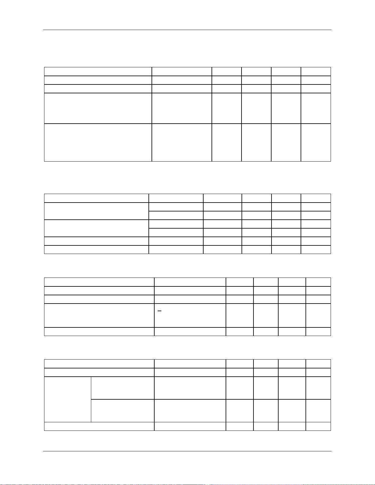
Data Sheet 71M6531D/F-71M6532D/F FDS 6531/6532 005
Parameter
Condition
Min
Typ
Max
Unit
Digital high-level input voltagea, VIH
2 V
Digital low-level input voltagea, VIL
0.8
V
Other digital inputs
-1
0
Other digital inputs
-1
0
1
µA
Parameter
Condition
Min
Typ
Max
Unit
I
LOAD
= 1 mA
V3P3D–0.4
V
I
LOAD
= 15 mA
V3P3D-0.6
V
I
LOAD
= 1 mA
0 0.4
V
I
LOAD
= 15 mA
0.8
V
OPT_TX VOH (V3P3D-OPT_TX)
I
=1 mA
0.4
V
OPT_TX VOL
I
=20 mA
0.7
V
Load Resistor
27
45
63
kΩ
FIR_LEN[1:0]=0 (L=138)
(-10%)
-48.7
(+10%)
μV
FIR_LEN[1:0]=0 (L=186)
(-10%)
-19.8
(+10%)
μV
5.4 Performance Specifications
5.4.1 Input Logic Levels
Table 70: Input Logic Levels
Input pull-up current, IIL
E_RXTX,
E_RST, CKTEST
Input pull down current, IIH
ICE_E
RESET
PB
a
In battery powered modes, digital inputs should be below 0.3 V or above 2.5 V to minimize battery current.
VIN=0 V, ICE_E=1
10
10
VIN = V3P3D
10
10
-1
0
100
100
1
100
100
1
µA
µA
µA
µA
µA
µA
5.4.2 Output Logic Levels
Table 71: Output Logic Levels
Digital high-level output voltage VOH
Digital low-level output voltage VOL
SOURCE
SINK
5.4.3 Power-Fault Comparator
Table 72: Power-Fault Comparator Performance Specifications
Parameter Condition Min Typ Max Unit
Offset Voltage: V1-VBIAS -20 +15 mV
Hysteresis Current: V1 Vin = VBIAS – 100 mV 0.8 1.2 μA
+100 mV overdrive
Response Time: V1
Voltage at V1 rising
Voltage at V1 falling
WDT Disable Threshold: V1-V3P3A -400 -10 mV
10
8
37
100
100
µs
μs
5.4.4 Battery Monitor
Parameter Condition Min Typ Max Unit
LSB Value
Offset Error -200 0 +100
100 © 2005-2010 TERIDIAN Semiconductor Corporation v1.3
Table 73: Battery Monitor Performance Specifications (BME= 1)
[M40MHZ, M26MHZ]
= [00], [10], or [11]
[M40MHZ, M26MHZ]
= [01]
FIR_LEN[1:0]=1 (L=288)
FIR_LEN[1:0]=2 (L=384)
FIR_LEN[1:0]=1 (L=384)
FIR_LEN[1:0]=2 (L=588)
-5.35
-2.26
-2.26
-0.63
μV
μV
μV
μV
mV
 Loading...