

Page 1
3-Phase Energy Meter IC
DATA SHEET
A Maxim Integrated Products Brand
MPU
RTC
TIMERS
IA
VA
IB
VB
XIN
XOUT
VREF
RX
TX
V1
TX
RX
COM0..3
V2
V3
V3.3A V3.3D
VBAT
V2.5
VLCD
VBIAS
VDRV
IC
VC
SEG0..23
GNDA GNDD
SEG 24..27
DIO 0..11
SEG 32..41
DIO 12..21
ICE
LIVE
LIVE
LIVE
NEUTRAL
LOAD
88.88.8888
MISC
POWER
FAULT
Etc.
IR
AMR
EEPROM
BATTERY
COMPARATOR
SENSE
DRIVE
SERIAL PORTS
OSC/PLL
CONVERTER
LCD DRIVER
DIO, PULSE
COMPUTE
ENGINE
FLASH
RAM
VOLTAGE REF
32 kHz
REGULATOR
5V BOOST
CT /COIL
POWER SUPPLY
TERIDIAN
71M6513
3/5V LCD
TEMP SENSOR
19-5360; Rev 3; 9/11
Single C onv erter Techn o logy is a r egistered trademark of
GENERAL DESCRIPTION
The 71M6513 is a highly integrated system-on-chip SoC with an MPU core,
real-time clock (RTC), flash, and LCD driver. Our Single Converter
Technology® with a 21-bit delta-sigma ADC, six anal og inputs, digital temperature com pensation, precision volt age reference, and 32-bi t computation
engine (CE) supports a wide range of poly-phase metering applications with
very few lo w-cost external components. A 32kHz cr ystal time ba se for the
entire system and internal battery-backup support for RAM and RTC further
reduce system cost.
2
Maximum design flexibility is supported with multiple UARTs, I
fail comparator, a 5V LCD charge pump, up to 22 DIO pins, and an insystem programmable flash. The device is offered in high (0.1%) and
standard (0.5%) accuracy versions for multifunction residential/commercial
meter applications requiring multiple voltage/current inputs and complex
LCD or DIO configurations.
A complete array of ICE and development tools, programming libraries and
reference designs enable rapid development and certification of meters that
meet most demanding worldwide electricity metering standards.
C, a power-
71M6513/71M6513H
SEPTEMBER 2011
FEATURES
Wh Accuracy < 0.1% Over 2,000:1
Current Range
Exceeds IEC 62053/ANSIC 12.20
Voltage Reference
< 10ppm/°C (71M6513H)
< 40ppm/°C (71M6513)
Six Sensor Inputs—V
Auxiliary Analog Input for Neutral
Current
Low Jitter Wh/VARh Pulse Outputs
Pulse Count For Pul se Outputs
Four-Quadrant M etering
Phase Sequencing
Line Frequency Count for RTC
Digital Temper ature Compensation
Sag Detection
Independent 32-Bit Compute Engine
40-70Hz Line Frequenc y Range with
Same Calibration
Phase Compensation (±7°)
Battery Backup f or RAM and RTC
22mW at 3.3V , 7. 2µW Backup
Flash Memory Option with Security
8-Bit MPU (80515)—One Clock
Cycle per Instruction
LCD Driver (≤ 168 Pixels)
High-Speed SSI Serial Output
RTC for Time-of-Use Functions
Hardware Watchdog Timer
Up to 22 General-Purpose I/O Pins
64KB Flash, 7KB RAM
Two UARTs for IR and AMR
100-Pin LQFP Package
Referenced
DD
Maxim Int e grated Produc t s , Inc .
© 2005-2011 Teridian Semiconductor Corporation Page: 1 of 104
Page 2

71M6513/71M6513H
3-Phase Energy Meter IC
DATA SHEET
A Maxim Integrated Products Brand
Table of Contents
FEATURES ............................................................................................................................ 1
HARDWARE DESCRIPTION ................................................................................................................ 9
Hardware Overview ................................................................................................................. 9
Analog Front End (AFE) .......................................................................................................... 9
Multiplexer................................................................................................................. 9
ADC .......................................................................................................................... 10
FIR Filter ................................................................................................................... 10
Voltage Reference ..................................................................................................... 10
Temperature Sensor .................................................................................................. 11
V3 ............................................................................................................................. 11
Functional Description ............................................................................................... 11
Com putat ion En gine (C E) ........................................................................................................ 12
Meter Equations ........................................................................................................ 12
Pulse Generator ........................................................................................................ 13
Real-Time Monitor ..................................................................................................... 13
CE Functional Overview ............................................................................................ 13
80515 MPU Core .................................................................................................................... 16
80515 Overview ........................................................................................................ 16
Memory Organization ................................................................................................ 16
Special Function Registers (SFRs) ............................................................................. 18
Special Function Registers (Generic 80515 SFRs) ..................................................... 19
Special Function Registers Specific to the 71M6513 ................................................... 22
Instruction Set ........................................................................................................... 23
UART ........................................................................................................................ 23
Timers and Counters ................................................................................................. 26
WD Timer (Software Watchdog Timer) ....................................................................... 28
Interrupts ................................................................................................................... 31
External Interrupts ..................................................................................................... 34
Interrupt Priorit y Level S t ructure ................................................................................. 35
Interru pt Sources and Vect ors .................................................................................... 37
On-Chip R esour ces ................................................................................................................. 39
DIO Ports .................................................................................................................. 39
AUGUST 2011
Page: 2 of 104 © 2005-2011 Teridian Semiconductor Corporation
Page 3

71M6513/71M6513H
3-Phase Energy Meter IC
DATA SHEET
A Maxim Integrated Products Brand
Physical Mem ory ....................................................................................................... 41
Oscillator ................................................................................................................... 42
Real-Time Clock (RTC).............................................................................................. 42
Comparators (V2, V3) ................................................................................................ 42
LCD Drivers .............................................................................................................. 43
LCD Voltage Boost Circuitry....................................................................................... 43
UART (UART0) and Optical Port ( UA RT1).................................................................. 44
Hardware Reset Mechanisms .................................................................................... 44
Reset Pin (RESETZ).................................................................................................. 44
Hardware Watchdog Timer ........................................................................................ 44
Crystal Frequency Monitor ......................................................................................... 44
V1 Pin ....................................................................................................................... 44
Internal Clocks and Clock Dividers ............................................................................. 45
I2C In terface (EE PROM) ........................................................................................... 45
Battery ...................................................................................................................... 47
Internal Voltages (VBIAS, VBAT, V2P5) ..................................................................... 47
Test Ports ................................................................................................................. 47
FUNCTIONAL DESCRIP TION .............................................................................................................. 49
Theory of Operation ................................................................................................................ 49
System Timing Summary......................................................................................................... 50
Data Flow ............................................................................................................................... 52
CE/MPU Communicati o n ......................................................................................................... 52
Fault, Reset, Power-Up ........................................................................................................... 53
Battery Operation .................................................................................................................... 54
Power Save Modes ................................................................................................................. 54
Chopping Circuitry ................................................................................................................... 55
Internal/External Pulse Generation and Pulse Counting ............................................................ 57
Program Security .................................................................................................................... 58
FIRMWARE INTERFACE ..................................................................................................................... 59
I/O RAM MAP – In Numerical Order ......................................................................................... 59
SFR M A P (SFRs Speci f ic to T eridian 80515) – In Numerical Order ........................................... 60
I/O RAM (Confi g ur a tion RAM) – Alphabetical Order.................................................................. 61
CE Program and Environment ................................................................................................. 67
CE Program .............................................................................................................. 67
Formats..................................................................................................................... 67
SEPTEMBER 2011
© 2005-2011 Teridian Semiconductor Corporation Page: 3 of 104
Page 4

71M6513/71M6513H
3-Phase Energy Meter IC
DATA SHEET
A Maxim Integrated Products Brand
Constants .................................................................................................................. 67
Environment .............................................................................................................. 67
CE Calculations ......................................................................................................... 68
CE RAM Locations .................................................................................................... 68
CE Front End Data (Raw Data) .................................................................................. 69
CE Status Word......................................................................................................... 69
CE Transfer Variables ............................................................................................... 70
TYPICAL PERFORMANCE DATA......................................................................................................... 77
Wh Ac curacy at Room Temperature ........................................................................................ 77
VARh Accuracy at Room Temperature .................................................................................... 77
Harmonic Performance ............................................................................................................ 78
APPLICATION INFORMATION ............................................................................................................. 79
Connection of Sensors (CT, Resistive Shunt, Rogowski Coil) ................................................... 79
Distinction between 71M6513 and 71M6513H Parts ................................................................. 79
Temperature Compensation and Mains Frequency Stabilization for the RTC............................. 80
External Temperature Compensation ....................................................................................... 81
Temperature Measur ement ..................................................................................................... 81
Crystal Oscillator ..................................................................................................................... 83
Connecting LCDs .................................................................................................................... 84
Connecting I2C EEPROMs ...................................................................................................... 85
Connectin g 5V Devices ........................................................................................................... 85
Optical Interface ...................................................................................................................... 87
Connecting V1 and Reset Pins ................................................................................................ 87
Connecting the V3 Pin ............................................................................................................. 88
Connecting a Battery ............................................................................................................... 88
Flash Programming ................................................................................................................. 89
MPU Firmware Library............................................................................................................. 89
SPECIFICATIONS ................................................................................................................................ 90
Electrical Specifications ........................................................................................................... 90
LOGIC LEVELS......................................................................................................... 91
VREF, VBIAS ............................................................................................................ 93
CRYSTAL OSCILLATOR ........................................................................................... 93
LCD BOOST ............................................................................................................. 95
LCD DRIVERS .......................................................................................................... 95
RTC .......................................................................................................................... 95
AUGUST 2011
Page: 4 of 104 © 2005-2011 Teridian Semiconductor Corporation
Page 5

71M6513/71M6513H
3-Phase Energy Meter IC
DATA SHEET
A Maxim Integrated Products Brand
SEPTEMBER 2011
RESETZ.................................................................................................................... 95
COMPARATORS ...................................................................................................... 96
RAM AND FLASH MEMORY ..................................................................................... 96
FLASH MEMORY TIMING ......................................................................................... 96
EEPROM INTERFACE .............................................................................................. 96
Recommended Exter nal Components ...................................................................................... 97
Packaging Information ............................................................................................................. 98
Pinout (Top View) ...................................................................................................... 99
Pin Descriptions ........................................................................................................ 100
I/O Equivalent Circuits: .............................................................................................. 102
ORDERING INFORMATION ................................................................................................... 103
Figures
Figure 1: IC Functional Block Diagram .......................................................................................................................... 8
Figure 2: General Topology of a Chopped Amplifier ..................................................................................................... 10
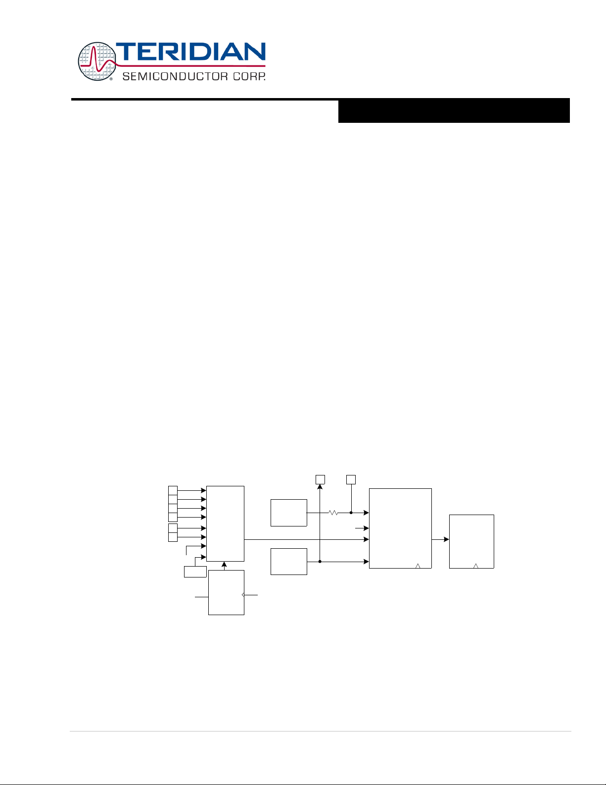
Figure 3: AFE Block Diagram...................................................................................................................................... 11
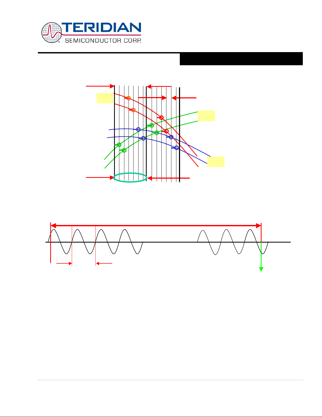
Figure 4: Samples in Multiplexer Cycle ....................................................................................................................... 14
Figure 5: Accumulation Interval.................................................................................................................................. 14
Figure 6: Memory Map .............................................................................................................................................. 16
Figure 7: Interrupt Structure ...................................................................................................................................... 38
Figure 8: DIO Ports Block Diagram ............................................................................................................................. 39
Figure 9: Oscillator Circuit ......................................................................................................................................... 42
Figure 10: LCD Voltage Boost Circuitry ....................................................................................................................... 43
Figure 11: Voltage Range for V1 ................................................................................................................................ 45
Figure 12: Voltage. Current, Momentary and Accumulated Energy................................................................................ 49
Figure 13: Timing Relationship between ADC MUX, CE, and Serial Transfers ................................................................ 50
Figure 14: RTM Output Format .................................................................................................................................. 51
Figure 15: SSI Timing, (SSI_FPOL = SSI_RDYPOL = 0) ............................................................................................ 51
Figure 16: SSI Timing, 16-bit Field Example (External Device Delays SRDY) ................................................................. 51
Figure 17: MPU/CE Data Flow .................................................................................................................................... 52
Figure 18: MPU/CE Communication (Functional) ......................................................................................................... 53
Figure 19: MPU/CE Communication (Processing Sequence) ........................................................................................ 53
Figure 20: Timing Diagram for Voltages, Current and Operation Modes after Power-Up ................................................. 54
Figure 21: Chop Polarity w/ Automatic Chopping ........................................................................................................ 56
Figure 22: Sequence with Alternate Multiplexer Cycles ................................................................................................ 56
Figure 23: Sequence with Alternate Multiplexer Cycles and Controlled Chopping ........................................................... 57
Figure 24: Wh Accuracy, 0.3A - 200A/240V ................................................................................................................ 77
Figure 25: VARh Accuracy for 0.3A to 200A/240V Performance ................................................................................... 78
Figure 27: Meter Accuracy over Harmonics at 240V, 30A ............................................................................................ 78
Figure 29: Resistive Voltage Divider (left), Current Transformer (right) ......................................................................... 79
Figure 30: Resistive Shunt (left), Rogowski Coil (right) ............................................................................................... 79
Figure 31: Crystal Frequency over Temperature .......................................................................................................... 80
Figure 32: Crystal Compensation ............................................................................................................................... 81
Figure 33: Error Band for VREF over Temperature (Regular-Accuracy Parts)................................................................. 83
© 2005-2011 Teridian Semiconductor Corporation Page: 5 of 104
Page 6

3-Phase Energy Meter IC
DATA SHEET
A Maxim Integrated Products Brand
Tables
71M6513/71M6513H
AUGUST 2011
Figure 34: Error Band for VREF over Temperature (High-Accuracy Parts) ..................................................................... 83
Figure 33: Connecting LCDs ...................................................................................................................................... 84
Figure 34: LCD Boost Circuit...................................................................................................................................... 85
Figure 35: EEPROM Connection ................................................................................................................................. 85
Figure 36: Interfacing RX to a 0-5V Signal .................................................................................................................. 86
Figure 37: Connection for Optical Components ........................................................................................................... 87
Figure 38: Voltage Divider for V1 ............................................................................................................................... 87
Figure 39: External Components for RESETZ .............................................................................................................. 88
Tab le 1: In puts Selected in Reg ular and Alternate Multiplexer Cyc les.......................................................... 9
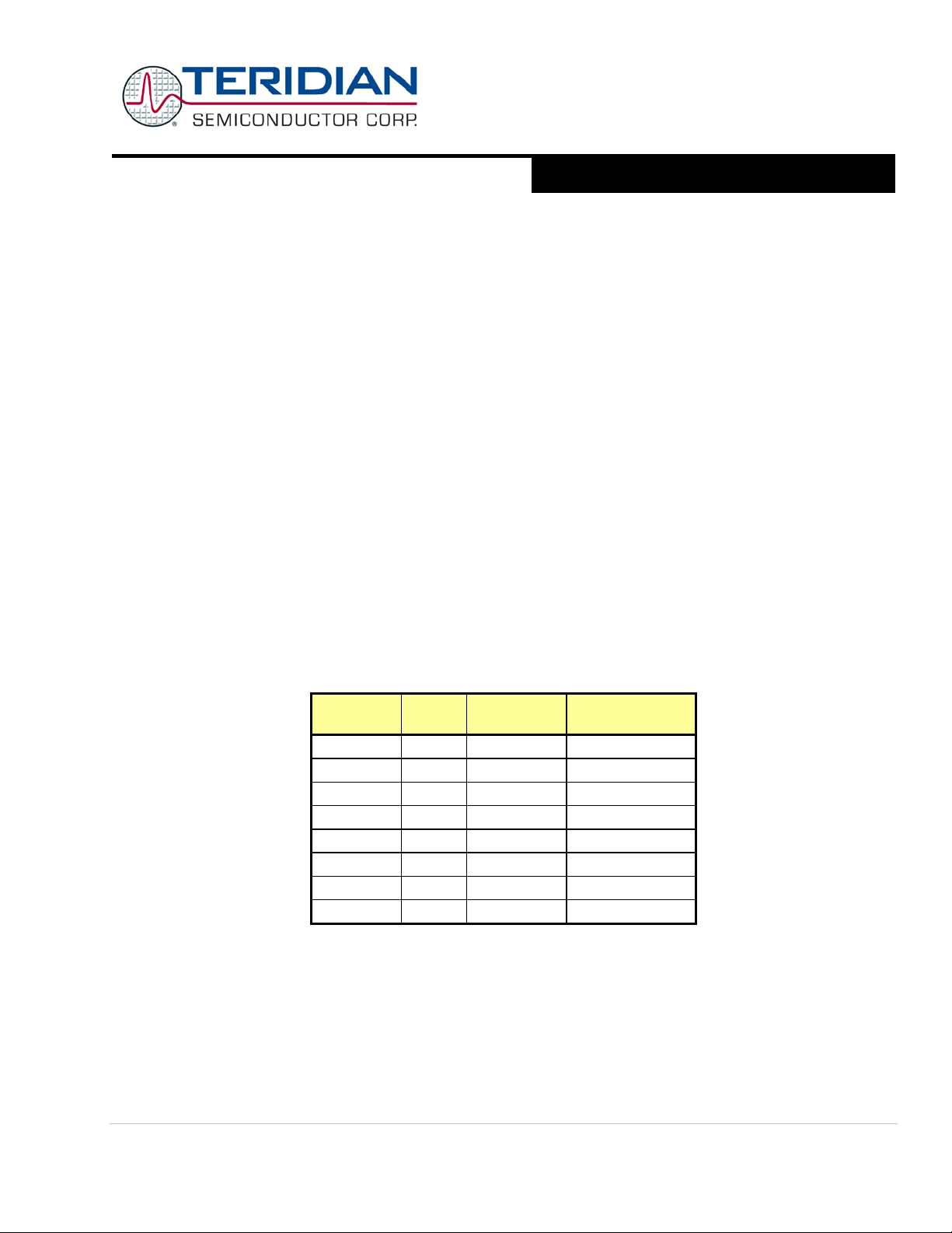
Table 2: CE DRAM Locations for ADC Results ......................................................................................... 12
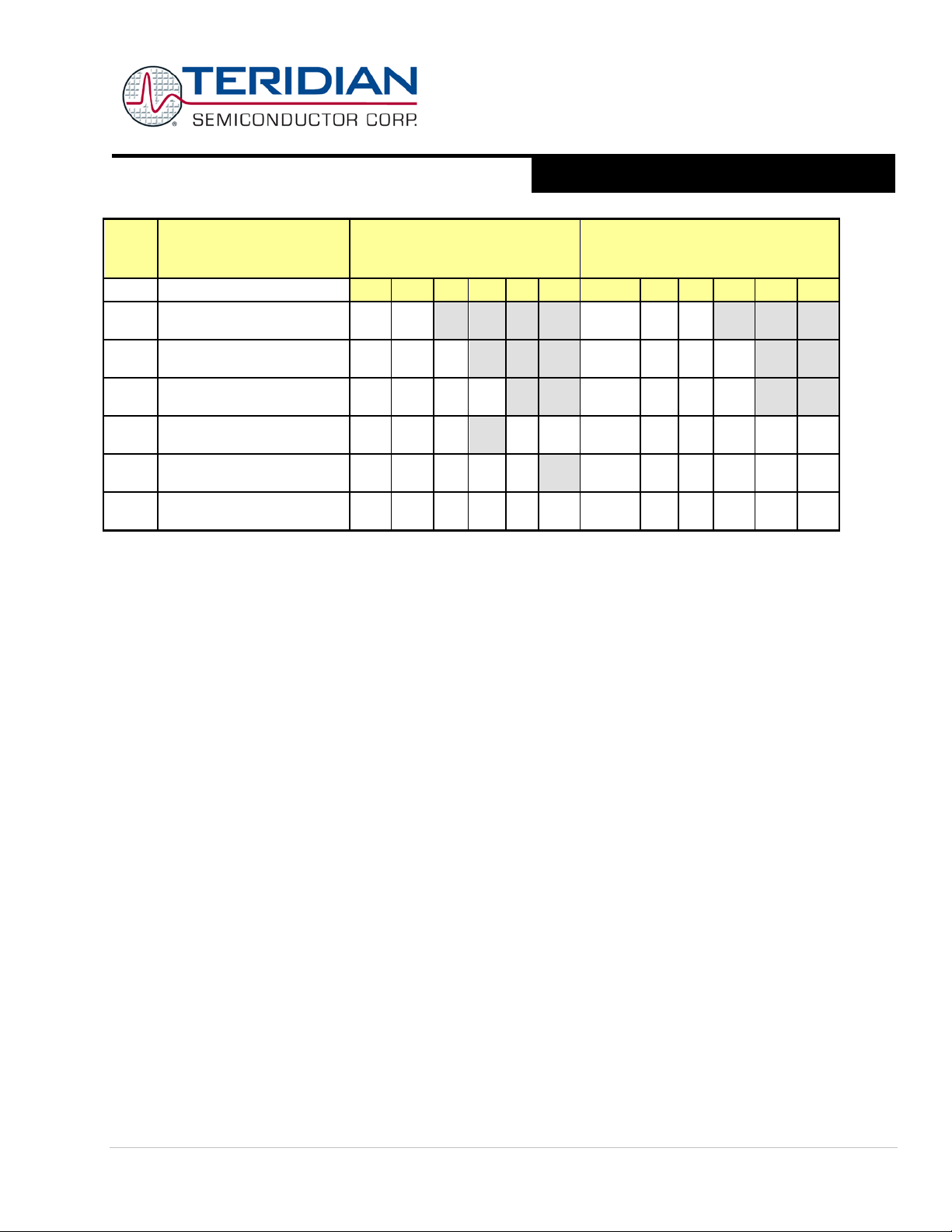
Table 3: Standard Meter Equations (inputs shown gray are scanned but not used for calculation) .............. 13
Tab le 4: St retch Memory Cycle Width ...................................................................................................... 17
Table 5: Internal Data Memory Map ......................................................................................................... 18
Table 6: Special Function Registers Locations ......................................................................................... 18
Table 7: Special Function Registers Reset Values .................................................................................... 20
Tab le 8: PSW Regi ster Fl ags ................................................................................................................... 20
Table 9: PSW bit functions ...................................................................................................................... 21
Tab le 10: Port Reg isters .......................................................................................................................... 22
Table 11: Specia l Funct ion Regist ers ....................................................................................................... 23
Table 12: Baud Rate Generation.............................................................................................................. 24
Table 13: UART Modes ........................................................................................................................... 24
Table 14: The S0CON Register ................................................................................................................. 24
Table 15: The S1CON register .................................................................................................................. 25
Table 16: The S0CON Bit Functions.......................................................................................................... 25
Table 17: The S1CON Bit Functions.......................................................................................................... 26
Tab le 18: The TMOD Register ................................................................................................................. 26
Tab le 19: TMOD Reg i ster Bi t Descripti on ................................................................................................. 27
Tab le 20: Timers/Counters M ode Description ........................................................................................... 27
Table 21: The TCON Register .................................................................................................................. 27
Table 22: The TCON Register Bit Functions ............................................................................................. 28
Table 23: Timer Modes............................................................................................................................ 28
Tab le 24: The PCON Register ................................................................................................................. 28
Tabl e 25: The IEN0 R egister (s ee also T able 32) ...................................................................................... 29
Table 26: The IEN0 Bit Functions (see also Table 32) ............................................................................... 29
Tab le 27: The IEN1 Regis ter (s ee also Tables 30/31) ............................................................................... 29
Table 28: The IEN1 Bit Functions (see also Tables 30/31) ........................................................................ 29
Tab le 29: The IP0 Register (s ee also T able 45) ........................................................................................ 30
Table 30: The IP0 bit Functions (see also Table 45) ................................................................................. 30
Tab le 31: The WDTR EL Regi ster ............................................................................................................. 30
Table 32: The WDTREL Bit Functions ...................................................................................................... 30
Table 33: The IEN0 Register .................................................................................................................... 32
Table 34: The IEN0 Bit Functions ............................................................................................................. 32
Table 35: The IEN1 Register ................................................................................................................... 32
Table 36: The IEN1 Bit Functions ............................................................................................................ 32
Table 37: The IEN2 Register ................................................................................................................... 33
Table 38: The IEN2 Bit Functions ............................................................................................................ 33
Page: 6 of 104 © 2005-2011 Teridian Semiconductor Corporation
Page 7

71M6513/71M6513H
3-Phase Energy Meter IC
DATA SHEET
A Maxim Integrated Products Brand
SEPTEMBER 2011
Table 39: The TCON Register .................................................................................................................. 33
Table 40: The TCON Bit Functions ........................................................................................................... 33
Table 41: The IRCON Register ................................................................................................................. 33
Table 42: The IRCON Bit Fun ctio ns .......................................................................................................... 34
Tab le 43: External MPU Interrupts ........................................................................................................... 34
Table 44: Control Bits for External Interrupts ............................................................................................ 35
Table 45: Priority Level Groups ................................................................................................................ 35
Tab le 46: The IP0 Register: ..................................................................................................................... 36
Tab le 47: The IP1 Register: ..................................................................................................................... 36
Table 48: Priority Levels .......................................................................................................................... 36
Table 49: Interrupt Polling Sequence ....................................................................................................... 36
Tab le 50: I nterr upt Vec tors ...................................................................................................................... 37
Tab le 51: Data Regist ers, Direction Register s and Internal Reso urces for DIO Pin Groups ........................ 39
Table 52: DIO_DIR Control Bit ................................................................................................................. 40
Tab le 53: Selectable C ontrols using th e DIO_DIR Bits .............................................................................. 40
Table 54: MPU Data Memory Map ........................................................................................................... 41
Tab le 55: Liqui d Crystal Display Segment Tabl e (Typical) ......................................................................... 43
Table 56: EECTRL Status Bits .................................................................................................................. 46
Tabl e 57: TMUX[3:0] Selections .............................................................................................................. 47
Tab le 58: SSI Pin A ssignment ................................................................................................................. 48
Table 59: Power Saving Measures........................................................................................................... 54
Table 60: CHOP_EN Bits.......................................................................................................................... 55
Tab le 61: Frequen cy ov er Temperature ................................................................................................... 80
© 2005-2011 Teridian Semiconductor Corporation Page: 7 of 104
Page 8
71M6513/71M6513H
3-Phase Energy Meter IC
DATA SHEET
A Maxim Integrated Products Brand
IA
VA
IB
VB
MUX
XIN
XOUT
VREF
CKTEST
CE
32-bit Compute
Engine
MPU
(80515)
CE
CONTROL
OPT_RX
OPT_TX
RESETZ
V1
EMULATOR
PORT
CE_BUSY
OPTICAL
I/F
UART
TX
RX
XFER BUSY
CE PROG
RAM
(4KB)
COM0..3
LCD DISPLAY
DRIVER
RTC
DATA
00-FF
PROG
000-7FF
DATA
0000-FFFF
PROG
0000-FFFF
MPU XRAM
(2KB)
0000-07FF
DIGITAL I/O
CONFIG
RAM
(I/O RAM)
2000-20FF
I/O RAM
CE DATA
RAM
(1KB)
MEMORY
SHARE
3000-3FFF
1000-13FF
RTCLK
RTCLK
MUX_SYNC
CKCE
CKMPU
V2
V3
CE_RUN
CE_LOAD
CE_EN
RTM_EN
COMP_INT
COMP_STAT
POWER FAULT
GENERATOR AND
COMPARATORS
LCD_EN
LCD_CLK
LCD_MODE
DIO_GP
RTC_SET
4.9MHz
4.9MHz
GNDD
V3P3A
V3P3D
VBAT
VOLT
REG
2.5V to logic
V2P5
MPU_DIV
SUM_CYCLES
PRE_SAMPS
EQU
CKOUT_EN
VLCD
TMUXOUT
FAULTZ
WAKE
VBIAS
DMUX
TMUX
CONFIGURATION
PARAMETERS
VDRV
GNDA
IC
TEMP
September 19, 2005
CK_GEN
OSC
(32KHz)
OSC_DIS
CK32
CK_EN
MCK
PLL
VOLTAGE
BOOST
LCD_BSTEN
LCD_IBST
VREF
VREF_DIS
MUX
CTRL
MUX_DIV
CHOP_EN
EQU
STRT
VC
MUX
CKFIR
4.9MHz
V3
MUX_SYNC
RTM
RTM
SEG20..23
DIO_0..3
SEG28/DIO8 ..
SEG31/DIO11
GNDA
GNDD
WPULSE
VARPULSE
WPULSE
VARPULSE
TEST
LCD_FS
LCD_MODE
LCD_EN
GNDD
LCD_NUM
DIO_OUT
DIO_IN
LCD_NUM
RTC_HOLD
0
1
2
3
4
5
6
7
8
9
A
B
C
D
E
F
DGND
IBIAS
WDTR_EN
V2 OK
V3 OK
OPTRX
ANALOG
DIGITAL
PULSEV/W
MUX_ALT
SEG24/DIO4 ..
SEG27/DIO7
SEG32/DIO12 ..
SEG41/DIO21
SCL
SDA
FLASH
(64KB)
EEWRSLOW
EERDSLOW
V3P3A
FIR_LEN
FIR
FILTER
CK_10M
CK_MPU
reserved
SEG0..2, SEG3/SCLK,
SEG4/SSDATA,
SEG5/SFR, SEG7..19
EEPROM
INTERFACE
DIO_EEX
PLL_2.5V
ECK_DIS
OPT_TXDIS
GNDD
∆Σ ADC
CONVERTER
+
-
VREF
RTCLK
CE_BUSY
XFER_BUSY
VBIAS
V3P3
V2P5
SEG6/SRDY
VBIAS
VBIAS
V3
CK32
SSI
AUGUST 2011
Page: 8 of 104 © 2005-2011 Teridian Semiconductor Corporation
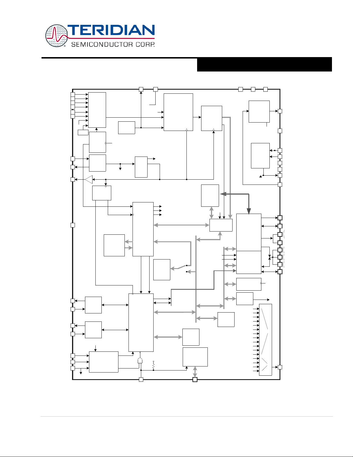
Figure 1: IC Functional Block Diagram
Page 9
71M6513/71M6513H
3-Phase Energy Meter IC
DATA SHEET
A Maxim Integrated Products Brand
SEPTEMBER 2011
HARDWARE DESCRIPTION
Hardware Overview
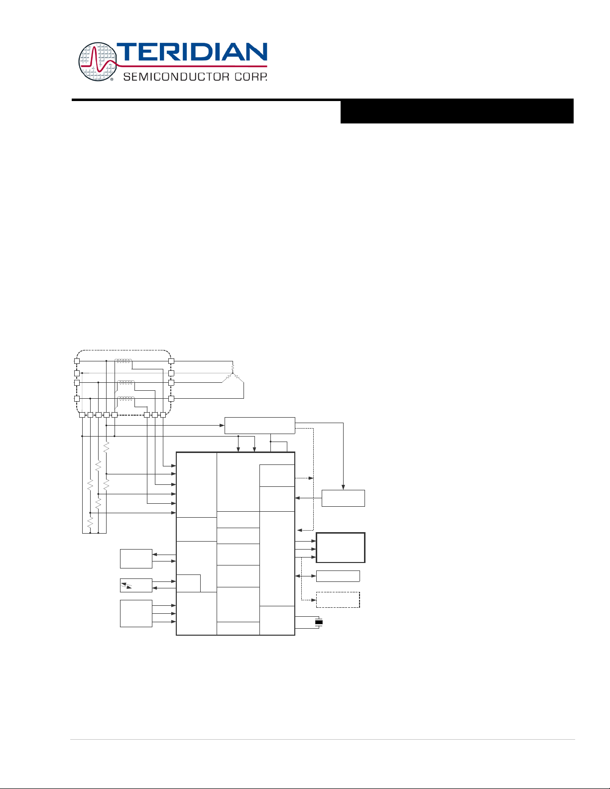
The 71M6513 single-chip polyphase meter integrates all primary functional blocks required to implement a solid-state
electricity meter. Included on chip are an analog front end (AFE), an 8051-com pa ti ble mi cr opr oc ess or ( MPU ) whi ch exec ut es
one instruction per clock cycle (80515), an independent 32-bit digital computation engine (CE), a voltage reference, a
tem peratur e senso r, LCD driver s, RAM, flash memory, a real time clock (RTC), and a variety of I/O pins. Various current
sensor technologies are supported including Curre nt Transfo r mers (CT), Resistive Shunts, and Rogowski (di/dt) Coils.
In addition to advanced m easurement functions, the real time clock function allows the 71M6513/6513H to record tim e of use
(TOU) metering information for multi-rate applications. Measurements can be displayed on either a 3V or a 5V LCD. Flexible
mapping of LCD display segments will facilitate integration with any LCD format. The design tr ade-off b et w een t h e n u m ber o f
LCD segments and DIO pins can be flexibly configured using memory-mapped I/O to accommodate various requirements.
The 71M6513 includes several I/O peripheral functions that improve the functionality of the device and reduce the component
count for most meter applications. The I/O peripherals include two UARTs, digital I/O, comparator inputs, LC D displ ay driver s ,
2
C int erface and an optic al/IR i nterf ace.
I
One of the two internal UARTs (UART1) is adapted to support an Infrared LED with internal drive output and sense input but it
can also function as a standard UART.
A block diagram of the chip is shown in Figure 1. A det ailed description of va r ious hardware blocks fol lows.
Analog Front End (AFE)
The AFE of the 71M6513 Power Meter IC is comprised of an input m ulti plexer, a del ta-sigma A/D converter with a voltage
ref erence, fol lowed by an FI R filter . A block diagram of t he AFE is shown i n Figure 3.
Multiplexer
The input multiplexer support s eight input signals that are applied to the pins IA, VA, IB, VB, IC, VC, and V3 plus the output of
the inter nal tempera ture sensor. The multiplexer can be operated in tw o modes:
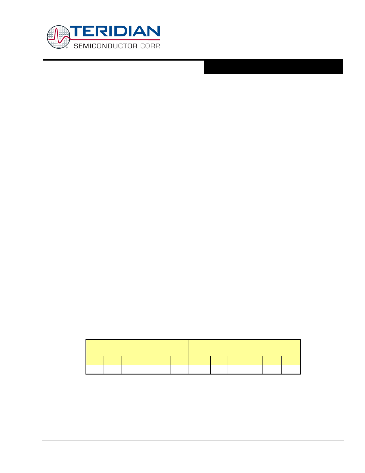
• Dur ing a nor mal mu l tiplexer cycle, t he signals from the six pi ns IA, VA , IB, VB, IC, and VC are s elect ed.
• During the alternate multiplexer cycle, the temperature signal (TEMP) and the additional monitor input, V3, are
selected, along with the other signal sources shown in Table 1: I nputs Selected in Regular and Alternate Multiplexer
Cycles.
Alt er nat e mul ti pl exer cy cles ar e us ual ly perf or m ed inf req uent l y (ev er y sec on d or so) . VA , VB , an d VC a re n ot r epl ac ed i n th e
alternate multiplexer cycles. In some equations, currents must be delayed in allpass networks and therefore cannot be
repl ac ed in th e al tern ate sel ect ion . Mis sin g sampl es du e to al tern ate m ulti plexer cyc les are a utomat ica lly i nter polated by the
CE.
Regular multiplexer sequence
Mux State:
0 1 2 3 4 5 0 1 2 3 4 5
IA VA IB VB IC VC TEMP VA V3 VB IC VC
Table 1: Inputs Selected in Regular and Alternate Multiplexer Cycles
In a typical application, the IA, IB, and IC inputs are connected to current transformers that sense the current on each phase of
the line voltage. VA, VB, and VC are typically connected to voltage sensors through resistor dividers.
The Multiplexer Control Circuit handles the setting of the multiplexer. The function of the Multiplexer Control Circuit is
governed by the I/O RAM registers MUX_ALT (0x2005[2]), EQU (0x2000[7:5]), and MUX_DIV (0x2002[7:6]). MUX_DIV controls
the number of samples per cycle. It can requ est 2, 3, 4, or 6 multiplexer states per cycle.
Alternate multiplexer sequence
Mux State:
© 2005-2011 Teridian Semiconductor Corporation Page: 9 of 104
Page 10
71M6513/71M6513H
3-Phase Energy Meter IC
DATA SHEET
A Maxim Integrated Products Brand
G
-
+V
inp
V
outp
V
outn
V
inn
CROSS
A
B
A
B
A
B
A
B
AUGUST 2011
The MUX_ALT bit requests an alternate multiplexer cycle. The bit may be asserted on any MPU cycle and may be subsequently de-asserted on any cycle including the next one. A rising edge on MUX_ALT will cause the Control Circuit to wait
until the next multiplexer cycl e and implement a sin gle alternate cycle.
Multiplexer Control Circuit also controls the FIR filt er initiation and the chopping of the ADC reference voltage, VREF. The
Mult iplexer Contro l Circuit is clocked by CK32, the 32768Hz clock from the PLL block, and launches each pass through the CE
program.
ADC
A single 21/22 -bit delta-sigma A/D converter digitizes the power inputs to the AFE. The resolution of the ADC is programmable
usi ng t he I/O RAM r egist er FIR_LEN register (0x2005[4]). ADC resolution may be selected to be 21 bits (FIR_LEN=0), or 22
bits (FIR_LEN=1). Convers ion time is tw o cycles of CK 32 with FIR_LEN = 0 and three cyc les wit h FIR_LEN = 1.
Accuracy, timing and functional spec ificatio ns in this data sheet are based on FIR_LEN = 0 (two CK32 cyc les).
Initiation of each ADC conversion is controlled by the Multiplexer Control Circuit as described previously.
FIR Filter
The finite impulse response (FIR) filter is an integral part of the ADC and it is optimized for us e with th e m ultipl exer. The
purpose of the FIR is to decimate the ADC output to the desired resolution. At the end of each ADC conversion, the output
data of the FIR filter (raw data) is stored into the CE DRAM location determined by the multiplexer selec ti o n. T he l oc ati on o f
the raw data in the CE DRAM is specified in the CE Program and Environment Section.
Voltage Reference
The 71M6513/6513H includes an on-chip precision bandgap voltage reference that incorporates auto-zero techniques. The
reference of the 71M6513H is trimm ed in production to minimize errors caused by component mismatch and drift. The result is
a voltage output with a predictable temperature coefficient.
The voltage reference is chopper stabilized, i.e. the polarity can be switched by the MPU using the I/O RAM register CHOP_EN
(0x2002[5:4]). The two bits in the CHOP_EN register enable the MPU to operate the chopper circuit in regular or inverted
operation, or in “toggling” mode. When the chopper circuit is toggled in between multiplexer cycles, DC offsets on the
measured signals will automatically be averaged out.
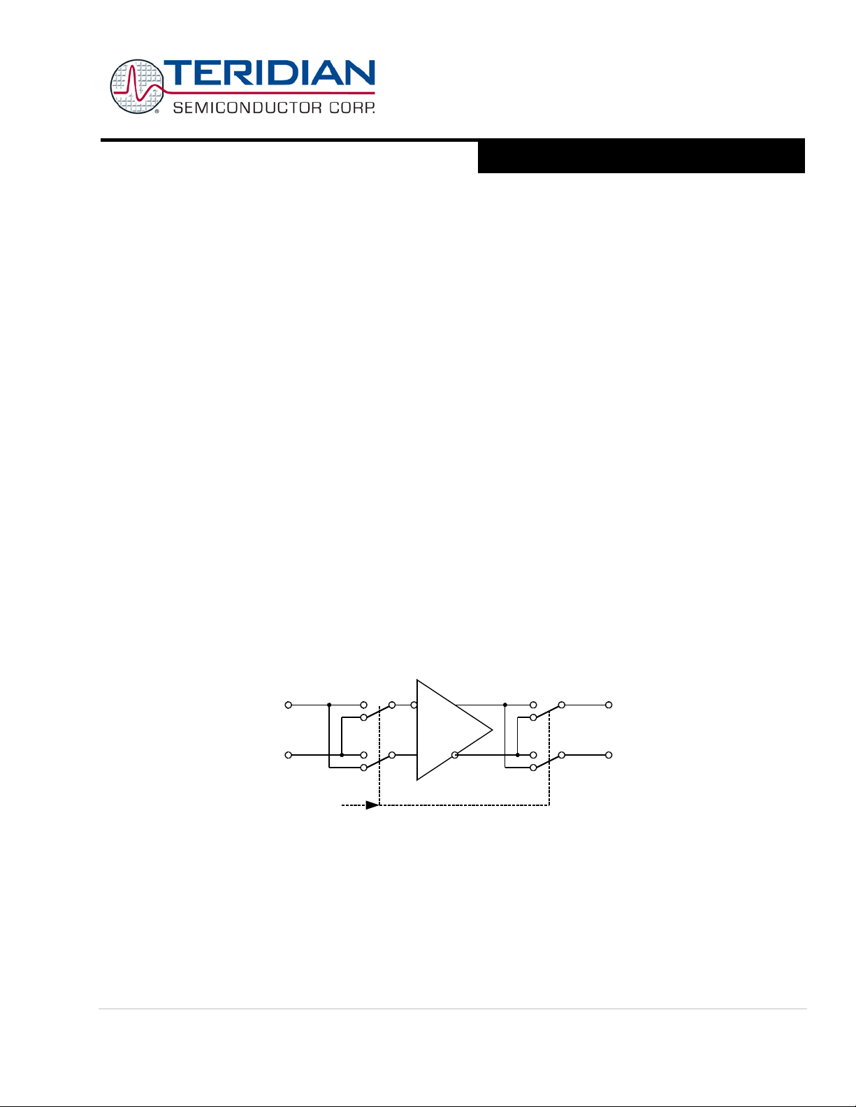
The general t opology of a chopped amplifier is given in Figure 2.
Figure 2: General Topology of a Chopped Amplifier
It is assumed that an offset voltage Voff appears at the positive amplifier input. With all switches, as controlled by CROSS in
the “A” position, the output voltage is:
Voutp – Voutn = G (Vinp + Voff – Vinn) = G (Vinp – Vinn) + G Voff
Page: 10 of 104 © 2005-2011 Teridian Semiconductor Corporation
Page 11
71M6513/71M6513H
3-Phase Energy Meter IC
DATA SHEET
A Maxim Integrated Products Brand
IA
VA
IB
VB
MUX
VREF
VBIAS
IC
VBIAS
(1.5V)
TEMP
CK32
VREF
VREF_DIS
MUX
CTRL
MUX_DIV
CHOP_EN
EQU
VC
MUX
V3
MUX_ALT
V3P3A
FIR_LEN
FIR
FILTER
∆Σ ADC
CONVERTER
+
-
VREF
SEPTEMBER 2011
With all switches set to the “B” position by applying the inverted CROSS signal, the output voltage is:
Voutn – Voutp = G (Vinn – Vinp + Voff) = G (Vinn – Vin p) + G Voff, or
Voutp – Voutn = G ( Vinp – Vinn) - G Voff
Thu s, when C ROSS i s toggled, e.g. af ter each multiplex er cyc le, the offset wil l alternately appear on the o utput as positiv e and
nega tiv e, which results in the offset ef fectively b eing el iminated, r egardless of its po larity or magnitu de.
The Functional Description Sec tion c ontains a ch apter with a det ailed description on control lin g t he CHOP_EN register.
Temperature Senso r
The 71M6513/6513H includes an on-chip temperature sensor implemented as a bandgap r efer ence. It i s us ed to determine
the die temperature The MPU may request an alternate multiplexer cycle containing the temperature sensor output by
asserting MUX_ALT.
The primary use of the temperature data is to determine the magnitude of compensation required to offset the thermal drift in
the system (see sec tio n t i tled “ Temperature Compensation”).
The z ero reference for the tem perature sen sor i s VBIAS.
V3
V3 is an additional analog monitor input that can be used for analog measurements, such as neutral current. It is sampled
when the multiplexer p erforms an alternate multiplexer cycle. The z ero reference for the V3 input is V BIAS.
V3 is also routed into the comparator block where it is compared to VBIAS. Comparator interrupts should be disabled when
the V3 input is used for analog measurements.
Functional Description
The AFE functions as a data acquisition system, controlled by the MPU. The main signals (IA, VA, IB, VB, IC, VC) are
sampled and the ADC counts obtained are stored in CE RAM where they can be accessed by the CE and, if necessary, by the
MPU. Alternate multiplexer cycles are initiated less frequently by the MPU to gather access to the slow signals, temperature
and V3.
© 2005-2011 Teridian Semiconductor Corporation Page: 11 of 104
Figure 3: AFE Block Diagram
Page 12
71M6513/71M6513H
3-Phase Energy Meter IC
DATA SHEET
A Maxim Integrated Products Brand
0x00
IA
V3P3
Pha se A cur rent
0x02
IB
V3P3
Pha se B cur rent
AUGUST 2011
Computation Eng ine (CE)
The CE, a dedicated 32-bit RISC processor, performs the precision computations necessary to acc urately m easure energy.
The CE calculations and processes include:
• Multiplication of each current sample with its associated voltage sample to obtain the energy per sample (when
multiplied with the constant sample time).
• Frequency-insensitive delay cancellation on all six channels (to compensate for the delay between samples caused
by the multiplexing scheme).
• 90° phase shifter (for VAR calculati ons).
• Pulse generation.
• Monitoring of the input signal frequency (for frequency and phase information).
• Monitoring of the input signal amplitude (for sag detection).
• Scaling of the processed samples based on chip temperature (temperature compensation) and calibration
coefficients.
The CE program RAM (CE PRAM) is loaded at boot time by the MPU and then executed by the CE. Each CE instruction word
is 2 bytes long. The CE program counter begins a pass through the CE code each time multiplexer state 0 begins. The code
pass ends when a HALT instruction is executed. For proper operation, the code pass must be completed before the
mul tiplexer cycle ends (see System Timing Summary in the Fun ctio nal Des cription Sec tion) .
The CE data RAM (CE DRAM) can be accessed by the FIR filter block, the RTM circuit, the CE, and the MPU. Assign ed time
sl ots are reserved for FIR, R TM, and MPU, respectively, such that m emory access es to CE_RAM do not collide. Holdi ng registers are used to convert 8-bit wide MPU data to/ from 32-bit wide CE DRAM data, and wait states are inserted as needed,
depending on the frequency of CKMPU.
Table 2 shows the CE DRAM addresses allocated to analog inputs from the AFE.
Address Name
0x01 VA V3P3 Phase A voltage
0x03 VB V3P3 Phase B voltage
0x04 IC V3P3 Phase C current
0x05 VC V3P3 Phase C voltage
0x06 TEMP VBIAS Temperature
0x07 V3 VBIAS V3 monitor
Table 2: CE DRAM Locations for ADC Results
Zero
Reference
Description
Meter Equations
The Compute Engine (CE) program for industrial m eter configurations implements the equations in Table 3. The I/O RAM
register EQU specifies the equation to be used based on the number and arrangement of phases used for metering. In case of
single and two-phase metering, the unconnected inputs should be tied to V3P3A, the analog supply voltage. The EQU
selection enables the 71M6513 to calculate polyphase power measurement based on the type of service used. Table 3 also
states t he sequence of t he multipl exer in t he AFE.
Page: 12 of 104 © 2005-2011 Teridian Semiconductor Corporation
Page 13
71M6513/71M6513H
3-Phase Energy Meter IC
DATA SHEET
A Maxim Integrated Products Brand
(1 element, 2W 1ø)
(1 element, 3W 1ø)
(2 element, 4W 3ø Delta)
(3 element, 4W 3ø Wye)
SEPTEMBER 2011
EQU
Watt & VAR Formula
0 1 2 3 4 5 0 1 2 3 4 5
VA IA
0
VA(IA-IB)/2
1
VA IA + VB IB
2
(2 element, 3W 3 øDelta)
VA (IA - IB)/2 + VC IC
3
VA(IA-IB)/2 + VB(IC-IB)/2
4
(2 element, 4W 3ø Wye)
VA IA + VB IB + VC IC
5
Table 3: Standard Meter Equations (inputs shown gray are scanned but not used for calculation)
Inputs used from MUX sequence
Mux State:
IA VA IB VB IC VC TEMP VA V3 VC IC VC
IA VA IB VB IC VC TEMP VA IB V3 VC VC
IA VA IB VB IC VC TEMP VA V3 VB VC VC
IA VA IB VB IC VC TEMP VA IB V3 IC VC
IA VA IB VB IC VC TEMP VA IB V3 IC VC
IA VA IB VB IC VC TEMP VA V3 VB IC VC
Inputs used from alternate MUX
sequence
Mux State:
Pulse Generator
The CE contains two pul se generato rs which cr eate low jitter pulses at a rate set by the CE D RAM reg isters APULSEW*WRATE
and APULSER*WRATE if EXT_PULSE (a CE input variable in CE DRAM) is 15. This mode puts the MPU in control of pulse
generation by placing values into the APULSEW and APULSER register s (“external puls e genera tio n”).
If EXT_PULSE is 0, APULSEW i s replaced with WSUM_X and APULSER is repla ced wit h VARSUM_X. In t his m ode, the CE
generates pulse based on its internal computation of WSUM_X and VARSUM_X, the signed sums of energy from all three
elements (“internal pulse generation”).
The DIO_PV and DIO_PW bit s as described in the Digital I/O section can be programmed to route W PULSE and VARPULSE
to the output pins DIO6 and DIO7 respectively. DIO6 and DIO7 can be configured to generate int errupts, which can be useful
for pulse counting by the MPU (see On-Chip Res ourc es, DIO Po rts sectio n).
Real-Time Monit or
The CE contains a Real Time Monitor (RTM), which can be programmed to monitor four selectable CE RAM l o cati on s at f ul l
sam ple rat e. The fo ur moni tored l ocatio ns are ser iall y output to the TM UXOUT pi n via t he digit al outp ut multi plexer at the
beginning of each CE code pass (see the Tes t Port s Section for details)
CE Functional Overview
The ADC processes on e sample p er c h an n el p er mul t i pl exer cy cl e. Figure 4 shows the timing of the six samples taken during
one multiplexer cycle.
The number of samples processed during one accumulation cycle is controlled by the I/O RAM registers PRE_SAMPS
(0x2001[7:6]) and SUM_CYCLES (0x2001[5:0]). The integration time for each energy output is
PRE_SAMPS * SUM_CYCLES / 2520.6, w here 25 20.6 i s the sample rate [Hz]
For examp le, PRE_SAMPS = 42 and SUM_CYCLES = 50 wil l establish 2100 samples per accumulati on cycle. PRE_SAMPS = 100
and SUM_CYCLES = 21 will res ult i n the exa ct s ame acc umulat ion c ycle of 2100 s amples or 833m s. Aft er an accumul ation
cycle is c omplet ed, th e X FER_B U SY interrupt sig nals to the MPU that accumulated da ta are avail able.
© 2005-2011 Teridian Semiconductor Corporation Page: 13 of 104
Page 14
71M6513/71M6513H
3-Phase Energy Meter IC
DATA SHEET
A Maxim Integrated Products Brand
VA
VB
IB
VC
IC
IA
1/2520.6Hz = 397µs
2/32768Hz =
61.04µs
13/32768Hz = 397µ s
per mux cycle
A
C
B
VA
VB
IB
VC
IC
IA
1/2520.6Hz = 397µs
2/32768Hz =
61.04µs
13/32768Hz = 397µ s
per mux cycle
A
C
B
XFER_BUSY
Interrupt to MPU
20ms
833ms
XFER_BUSY
Interrupt to MPU
20ms
833ms
AUGUST 2011
Figure 4: Sam ples in M ultip lexer C ycle
The en d of ea ch mul tiplex er cy cle is si gnal ed to t he MPU by the CE_ BUSY i nterr upt. At the end o f each m ultip lexer c ycl e,
status i nformation, such as sag data and the digitized input signal, is available to the MPU.
Figure 5 shows the accumulation interval resulting from PRE_SAMPS = 42 and SUM_CYCLES = 50, consisting of 2100 samples
of 397µs each (only one phase is shown) followed by the XFER_BUSY interrupt. The sampling in this example is applied to a
50Hz signal.
Ther e is no c orr el ati on bet ween t he l i ne si gn al fr equ enc y a nd t he ch oi ce of PRE_SAMPS or SUM_CYCLES (even though when
SUM_CYCLES = 42 one set of SUM_CYCLES happens to sample a period of 16.6ms). Furtherm or e, s am pl i ng d oes n ot h ave t o
start when the line voltage crosses the zero line.
Delay Compensation
When measuring the energy of a phase (i.e., Wh and VARh) in a service, the voltage and current for that phase must be
sampled at the same instant. Other w ise, the phase difference, Ф, introduces errors.
Page: 14 of 104 © 2005-2011 Teridian Semiconductor Corporation
Figure 5: Accumulation Interval
Page 15

71M6513/71M6513H
3-Phase Energy Meter IC
DATA SHEET
A Maxim Integrated Products Brand
o
delay
o
delay
ft
T
t
360360 ⋅⋅=⋅=
φ
SEPTEMBER 2011
Where f is the frequency of the input signal and t
In traditional meter ICs, sampling is accomplished by using two A/D converters per phase (one for voltage and the other one
for current) controlled to sample simultaneously. Our Single-Converter Technology, however, exploits the 32-bit signal
processing capability of its CE to implement “constant delay” all-pass filters. These all-pass filters correct for the conversion
time difference between the voltage and the corresponding current samples that are obtained with a single multiplexed A/D
converter.
The “constant delay” all-pass filters provide a broad-band delay β that is precisely matched to the difference in sam ple t im e
between the voltage and the current of a given phase. This digital filter does not affect the amplitude of the signal, but
pro vi des a prec i sel y co ntr oll ed p ha se r esp ons e. T he del a y com pen sat ion imp lem ent ed i n th e CE al i gns the v ol ta ge s ampl es
with their corresponding current samples by routing the voltage samples through the all-pass filter, thus delaying the voltage
samples by β, resulting in the residual phase error β – Ф. The residual phase error is negligible, and is typically less than ±1.5
milli-degrees at 100Hz, thus it does not contribute to errors in the energy measurements.
is th e sampling delay between voltage and current .
delay
© 2005-2011 Teridian Semiconductor Corporation Page: 15 of 104
Page 16
71M6513/71M6513H
3-Phase Energy Meter IC
DATA SHEET
A Maxim Integrated Products Brand
0xFFFF
0xFFFF
0x4000
0x3FFF
0x3000
0x2FFF
0x2100
0x20FF
0x2000
0x1FFF
0x1400
0x13FF
0x1000
0x0FFF
0x0800
0x07FF
0xFF
SFRs, RAM,
reg. banks
0x0000
0x0000
0x00
AUGUST 2011
80515 MPU Core
80515 Overview
The 71M6513/6513H includes an 80515 MPU (8-bit , 8051 -compatible) that processes most instructions in one clock cycle.
Using a 5MHz clock results in a processing throughput of 5 MIPS. The 80515 architecture eliminates redundant bus s ta tes and
implements parallel execution of fetch and execution phases. Normally a machine cycle is aligned with a memory fetch, therefore, most of the 1-byte instructions are performed in a single cycle. This leads to an 8x performance (in average)
improvement (in terms of MIPS) over t he Intel 8051 device running at t he sam e clock frequency.
Actual processor clocking speed can be adjusted to the total processing demand of the application (metering calculations,
AMR management, memory management, LCD driver management and I/O management) using the I/O RAM register
MPU_DIV[2:0].
Typical measurement and metering functions based on the results provided by the internal 32-bit com pute eng ine ( CE) are
available for the MPU as part of Teridian’s standard library. A standard ANSI “C” 80515-application programming interface
library is avai labl e to help reduce desi gn cycle.
Memory Organization
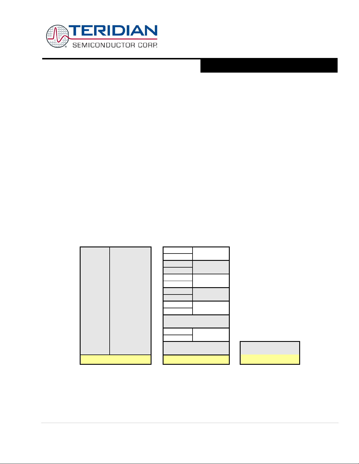
The 80515 MPU core incorporates the Harvard architecture with separate code and data spaces.
Memory organization in the 80515 is similar to that of the industry standard 8051. There are three memory areas: Program
memo ry (flash), external data memory (XRAM), physically consisting of XRAM, CE DRAM, CE PRAM and I/O RAM, and
internal data memory (Internal RAM). Figure 6 shows the memory map (see also Table 54).
Int er n al a nd Extern al D at a M em or y: Both internal and external data memory are physically located on the 71M6513 IC. External data memory is only external to the 80515 MPU core.
Flash memory
Progra m me mory External data memory Internal data memory
Progra m Memo ry: The 80515 can address up to 64KB of program memory space from 0x0000 to 0xFFFF. Program memory
is read when the MPU fetches instructions or performs a MOVC operation.
After res et, th e M PU starts program execution from location 0x00 00. T he lower part of the p r ogram memor y incl udes reset an d
interru pt vectors. The int errupt vectors are spac ed at 8-byte intervals, starting from 0x0003.
Ext ernal Data Mem ory: W hile the 80515 can address up to 64KB of external data memory in the space from 0x0000 to
0xFFFF, only the memory ranges shown in Figure 6 contain physical memory. The 80515 writes into external data memory
Page: 16 of 104 © 2005-2011 Teridian Semiconductor Corporation
---
CE PRAM
---
I/O RAM
---
CE DRAM
---
XRAM
Figure 6: Memory Map
Page 17
71M6513/71M6513H
3-Phase Energy Meter IC
DATA SHEET
A Maxim Integrated Products Brand
0 0 1 1 2 2 3
1
SEPTEMBER 2011
when the MPU executes a MOVX @Ri,A or MOVX @DPTR,A i nstruction. The MPU reads external data memory by executing
a MOVX A,@Ri or M OVX A,@DPTR instruction (SFR USR2 provides the upper 8 bytes for the MOVX A,@Ri instruction).
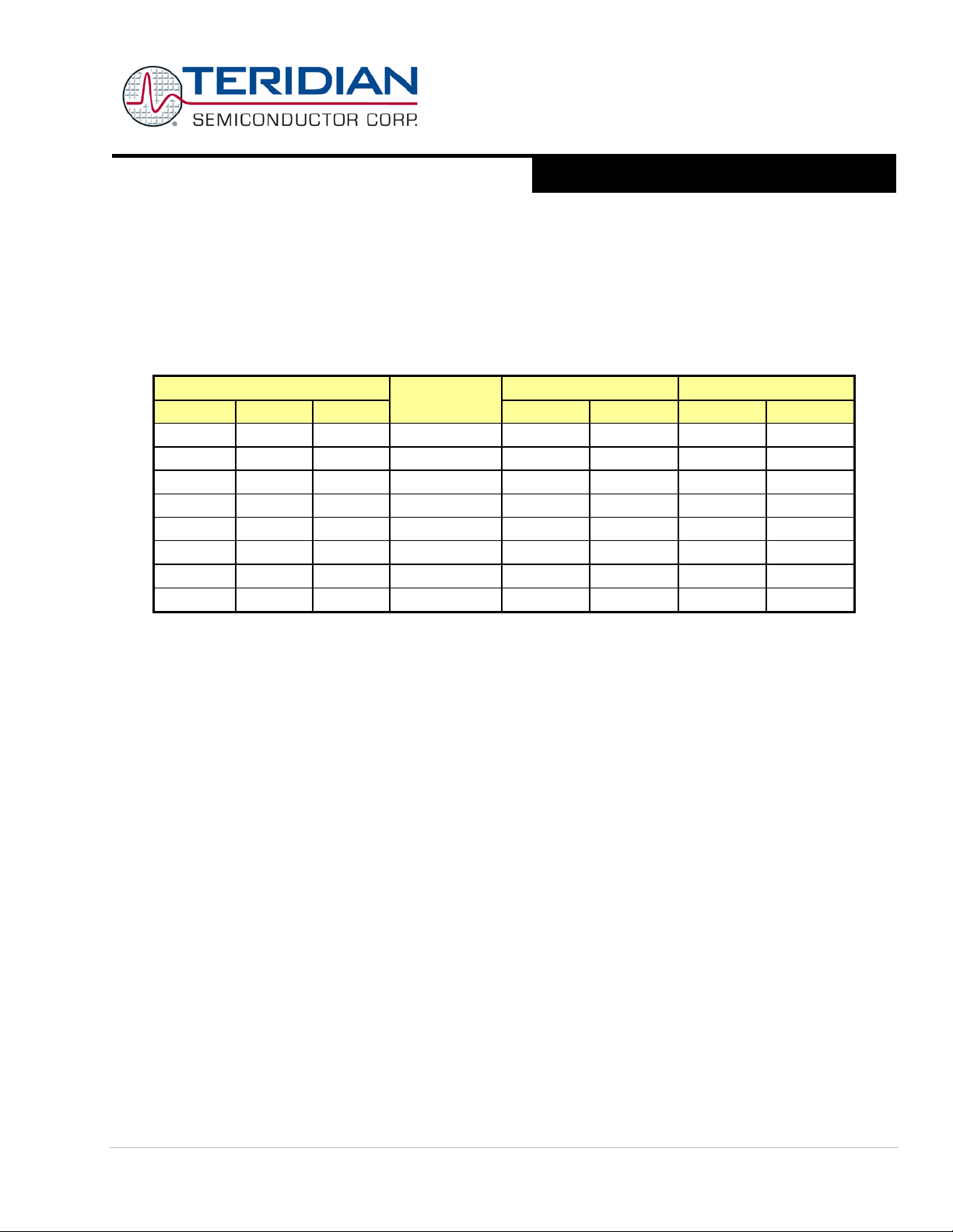
Clock Stretching: MOVX instructions can access fast or slow external RAM and external peripherals. The three low ordered
bits of the CKCON register define the stretch memory cycles. Setting all the CKCON st retch bits to one allows access to very
sl ow extern al RA M or exter nal peripherals.
Table 4 shows how the signals of the Ex ternal Memory Interface change when stretch values are set from 0 to 7. The widths of
the signals are counted in MPU clock cycles. The post-reset state of the CKCON register, which is in bold in the table,
performs the MOVX instructions with a stretch value equal to 1.
CKCON register Stretch Value Read signals width Write signal width
CKCON.2 CKCON.1 CKCON.0 memaddr memrd memaddr memwr
0 0 0 0 1 1 2 1
0 1 0 2 3 3 4 2
0 1 1 3 4 4 5 3
1 0 0 4 5 5 6 4
1 0 1 5 6 6 7 5
1 1 0 6 7 7 8 6
1 1 1 7 8 8 9 7
Table 4: Stretch M emory C ycle Width
There are two types of instructions, differing in whether they provide an eight-bit or s i xteen-bit indirect address to the external
data RAM.
In the first type (MOVX A,@Ri), the contents of R0 or R1, in t he current regist er bank, provide the eight l ower-ordered bits o f
address. The eight high-ordered bits of address are specified with the USR2 SFR. This method allows the user paged access
(256 pages of 256 bytes each) to the full 64KB of external data RAM. In the second type of MOVX instruction (MOVX
A,@DPTR), the dat a po i nt er g en er at es a s i xt een -bit address. This form is faster and more efficient when accessing very large
data arrays (up to 64 Kbytes), since no additional instructions are needed to set up the eight high ordered bits of address.
It is possible to m ix t he t wo MO VX t ypes . T his p rov id es t he us er wi th four s epar at e dat a p oint er s, t wo wi th d ir ect acc ess a nd
two with paged access to the entire 64KB of external memory range.
Dual Data Pointer: The Dual Data Pointer accelerates the block moves of data. The standard DPTR is a 16-bit register that i s
used to address external memory or peripherals. In the 80515 core, the standard data pointer is call ed DPTR, the second data
pointer is called DPTR1. The data pointer select bit chooses the active pointer. The dat a pointer select bit is locat ed at the LSB
of the DPS register (DPS.0). DPTR is selected when DPS.0 = 0 and DPTR1 is selected when DPS. 0 = 1.
The user switches between pointers by toggling the LSB of the DPS regi ster . A ll DPTR-related instructions use the currently
selected DPTR for any activity.
The second data pointer may not be supported by certain compilers.
© 2005-2011 Teridian Semiconductor Corporation Page: 17 of 104
Page 18
71M6513/71M6513H
3-Phase Energy Meter IC
DATA SHEET
A Maxim Integrated Products Brand
Address
Direct ad dressing
Indirect addressing
0x20
0x00
X000
X001
X010
X011
X100
X101
X110
X111
F8
INTBITS
FF
F0 B
F7
E8
WDI EF
E0 A
E7
D8
WDCON
DF
D0
PSW D7
C8
CF
C0
IRCON C7
B8
IEN1
IP1
S0RELH
S1RELH USR2
BF
B0
FLSHCTL
PGADR
B7
A8
IEN0
IP0
S0RELL
AF
A0
P2
DIR2
DIR0 A7
98
S0CON
S0BUF
IEN2
S1CON
S1BUF
S1RELL
EEDATA
EECTRL
9F
90
P1
DIR1
DPS
ERASE 97
88
TCON
TMOD
TL0
TL1
TH0
TH1
CKCON
8F
80
P0
SP
DPL
DPH
DPL1
DPH1
WDTREL
PCON
87
AUGUST 2011
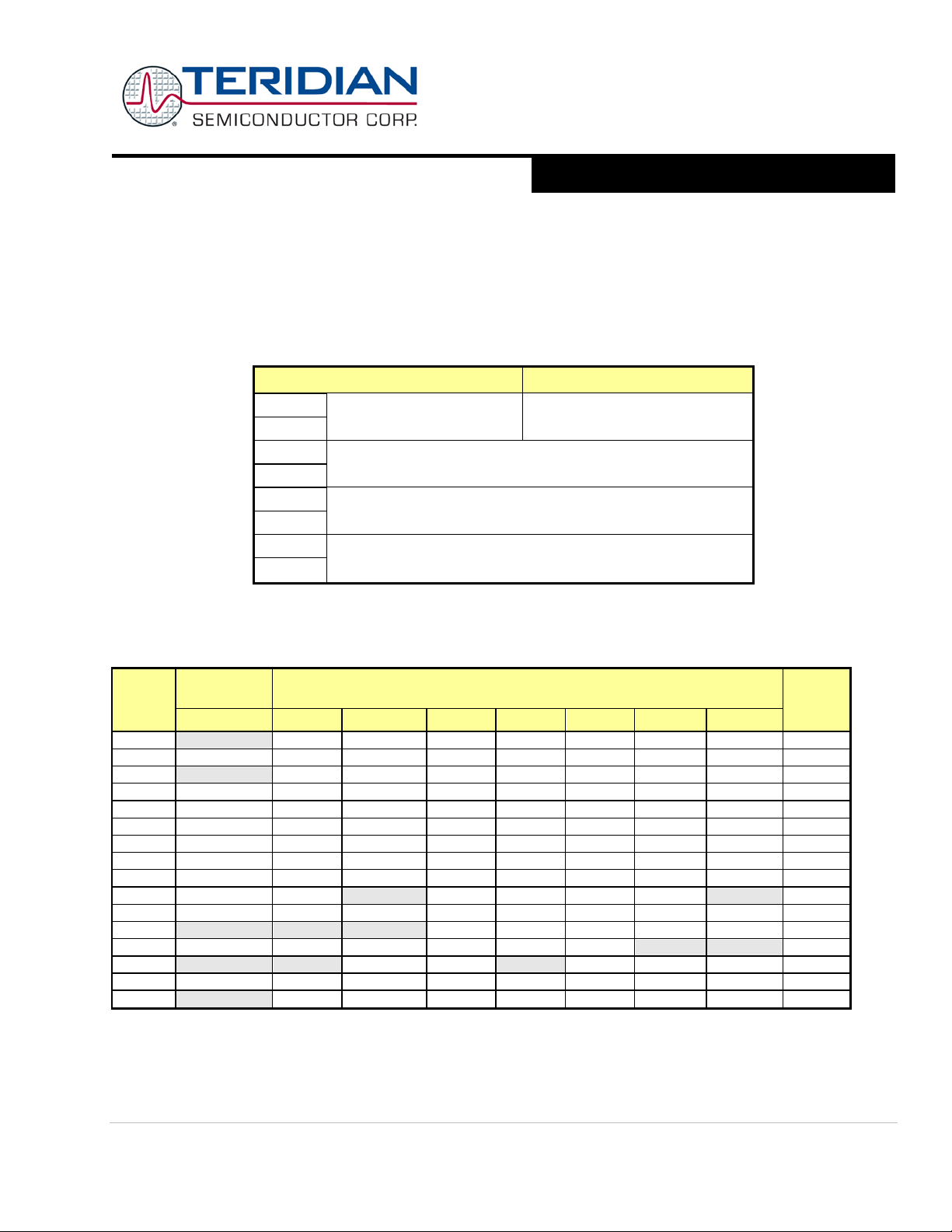
Int ernal Data Mem ory: The Internal data memory provides 256 bytes (0x00 to 0xFF) of data memory. The internal data
memory address is always 1 byte wide and can be accessed by either dir ect or indirect addressing. The Special Function
Registers occupy the upper 128 bytes. This SFR area is available only by direct addressing. Indirect addressing
accesses the upper 128 bytes of Internal RAM.
The lower 128 bytes contain working registers and bit-addressable memory. The lower 32 bytes form four banks of eight
registers (R0-R7). Two bits on the program memory status word (PSW) select which bank is in use. The next 16 bytes form a
blo ck of bit -addressa bl e memor y sp ace a t bi t add ress ees 0 x00-0x7F. All of the bytes in the lower 128 bytes are accessible
through direct or indirect addressing. Table 5 shows the internal data memory map.
0xFF
0x80
0x7F
0x30
0x2F
0x1F
Special Function Registers
(SFRs)
Byte-addressable area
Bit-ad dressable area
Register banks R0…R7
Table 5: Internal Data Memory Map
Special Function Regi st ers ( SFRs)
A map of the Special Function Registers is shown in Table 6.
Hex\Bin
Bit-address-
able
Byte-addressable
RAM
Bin/Hex
Table 6: Special Function Registers Locations
Only a few addresses are occupied, the others are not impl emented. SFRs specific to the 651X are shown in bold print. Any
read access to unimplemented addresses will return undefined data, while any w r i t e a cc es s wi l l h a ve n o ef f ec t . Th e r eg i s t er s
at 0x80, 0x88, 0x90, etc., are bit-addres sable, all others are byte-addressable.
Page: 18 of 104 © 2005-2011 Teridian Semiconductor Corporation
Page 19
71M6513/71M6513H
3-Phase Energy Meter IC
DATA SHEET
A Maxim Integrated Products Brand
P0
0x80
0xFF
Port 0
SP
0x81
0x07
St ack Poi nter
DPL
0x82
0x00
Data Pointer Lo w 0
DPH
0x83
0x00
Data Pointer High 0
DPL1
0x84
0x00
Data Pointer Lo w 1
DPH1
0x85
0x00
Data Pointer High 1
WDTREL
0x86
0x00
Watchdog Timer R eload register
PCON
0x87
0x00
UART Speed Control
TCON
0x88
0x00
Timer/Counter Control
TMOD
0x89
0x00
Timer Mode Control
TL0
0x8A
0x00
Timer 0, low byte
TL1
0x8B
0x00
Timer 1, high byte
TH0
0x8C
0x00
Timer 0, low byte
TH1
0x8D
0x00
Timer 1, high byte
CKCON
0x8E
0x01
Clock Control (Stretch=1)
P1
0x90
0xFF
Port 1
DPS
0x92
0x00
Data Pointer select R egist er
S0CON
0x98
0x00
Serial P or t 0, Con trol R egist er
S0BUF
0x99
0x00
Serial P or t 0, Data Buffer
IEN2
0x9A
0x00
Interrupt Ena ble Register 2
S1CON
0x9B
0x00
Serial P or t 1, Con trol R egist er
S1BUF
0x9C
0x00
Serial P or t 1, Data Buffer
S1RELL
0x9D
0x00
Serial P or t 1, Reload Regist er, low byte
P2
0xA0
0x00
Port 2
IEN0
0xA8
0x00
Interrupt Ena ble Register 0
IP0
0xA9
0x00
Interrupt Pri ority Regis ter 0
S0RELL
0xAA
0xD9
Serial P or t 0, Reload Regist er, low byte
P3
0xB0
0xFF
Port 3
IEN1
0xB8
0x00
Interrupt Ena ble Register 1
IP1
0xB9
0x00
Interrupt Pri ority Regis ter 1
S0RELH
0xBA
0x03
Serial P or t 0, Reload Regist er, hig h byte
S1RELH
0xBB
0x03
Serial P or t 1, Reload Regist er, hig h byte
Special Function Regi st ers ( Generic 80515 SFRs)
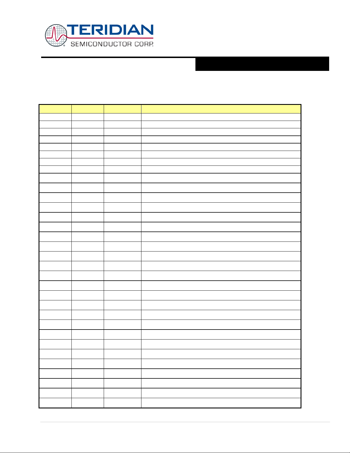
Table 7 shows the location of the SFRs and the value they assume at reset or power-up.
Name Location Reset value Description
SEPTEMBER 2011
© 2005-2011 Teridian Semiconductor Corporation Page: 19 of 104
Page 20
71M6513/71M6513H
3-Phase Energy Meter IC
DATA SHEET
A Maxim Integrated Products Brand
Name
Location
Reset value
Description
USR2
0xBF
0x00
User 2 Port, high address byt e for MOVX@Ri
IRCON
0xC0
0x00
Interrupt Request Co ntrol Register
PSW
0xD0
0x00
Program Status Word
WDCON
0xD8
0x00
Baud Rate C ontrol Register (only WD CON.7 b it used )
A
0xE0
0x00
Accumulator
B
0xF0
0x00
B Reg ister
AUGUST 2011
Table 7: Special Function Registers Reset Values
Accumulator (ACC, A): ACC is the accumulator register. Most instructions use the accumulator to hold the operand. The
mnemonics for accumulator-sp ecific instructi ons refer to accumulator as “A”, not ACC.
B Register: The B register is used during multiply and divide instructions. It can also be used as a scratch-pad register to hold
temporary data.
Program Status Word (PSW):
MSB LSB
CV AC F0 RS1 RS OV - P
Table 8: PSW Register Flags
Page: 20 of 104 © 2005-2011 Teridian Semiconductor Corporation
Page 21
71M6513/71M6513H
3-Phase Energy Meter IC
DATA SHEET
A Maxim Integrated Products Brand
PSW.7
CV
Carry flag
PSW.6
AC
in the
register.
RS1/RS0
Bank selected
Location
Parity flag, affected by hardware to indicate odd / even number of “one” bits in the
Bit Symbol Function
Auxiliary Carry flag for BCD operations
PSW.5 F0 G eneral purp ose Flag 0 available for user. Not to be confused with the F0 flag
CESTATUS
PSW.4 RS1 Register bank selec t control bits. The contents of RS1 and RS0 select the working
register bank:
SEPTEMBER 2011
PSW.3 RS0
PSW.2 OV Overflo w fla g
PSW.1 - User defined flag
PSW.0 P
Acc umulator, i .e. even pari ty.
Stack Pointer (SP): T he sta ck point er is a 1-byte regi ster ini tiali zed to 0x07 af ter r eset. This reg ister is inc remen ted befo re
PUSH and CALL instructions, causing the stack to begin at location 0x08.
Data Pointer: The data poi nter (DPTR) is 2 bytes wide. The lower part is DPL, and the highest is DPH. It can be loaded as a 2-
byt e r eg i st er ( MO V DPTR,# dat a 1 6) or as two r eg is t er s ( e. g . MOV DPL,#data8). It is generally used to access external code or
data space (e.g. MOVC A,@A+DPTR or MOVX A,@DPTR respectively).
Program Counter: The p rogram count er (PC) is 2 bytes wide initialized to 0x0000 after reset. This register is incremented
during the fetching operation code or when operating on data from program memory.
00 Bank 0 (0x00 – 0x07)
01 Bank 1 (0x08 – 0x0F)
10 Bank 2 (0x10 – 0x17)
11 Bank 3 (0x18 – 0x1F)
Table 9: PSW bit functions
© 2005-2011 Teridian Semiconductor Corporation Page: 21 of 104
Page 22
71M6513/71M6513H
3-Phase Energy Meter IC
DATA SHEET
A Maxim Integrated Products Brand
P0
0x80
R/W
Register for port 0 read and write operations (pins DIO0…DIO7)
DIR0
0xA2
R/W
Data direction register for port 0. Setting a bit to 1 m eans that the corresponding pin is
an output.
P1
0x90
R/W
Register for port 1 read and write operations (pins DIO8…DIO15)
DIR1
0x91
R/W
Data direction register for port 1.
P2
0xA0
R/W
Register for port 2 read and write operations (pins DIO16…DIO21)
DIR2
0xA1
R/W
Data direction register for port 2.
ERASE
FLSH_ERASE
0x94
W
(default =
Any other pattern written to FLSH_ERASE will hav e no effect.
PGADDR
FLSH_PGADR
0xB7
R/W
Must be re-written for eac h new Pag e Eras e cycle.
EEDATA
0x9E
R/W
I2C EEPRO M i nterf ace data register
EECTRL
0x9F
R/W
I2C EEPRO M i nterf ace con t rol reg ist er . If th e M P U wish es to write a
0xB2
R/W
Bit 0 (FLSH_PWE): Pro gram Wri te Enable:
AUGUST 2011
Port Registers: The I/O ports are controlled by Special Function Registers P0, P1 , and P2. The contents of the SFR can be
observed on corresponding pins on the chip. Writing a ‘1’ to any of the ports (see Table 10) causes the corresponding pin t o
be at high level (V3P3), and writing a ‘0’ causes the corresponding pin to be held at low level (GND). The data direction
registers DIR0, DIR1, and DIR2 define individual pins as input or output pins (see section On-Chip Resou rces , DIO Ports for
details).
Register SFR
Address
All four ports on the chip are bi-directional. Each of them consists of a Latch (SFR ‘P0’ to ‘P3’), an output driver, and an input
buffer, therefore the MPU can output or read data through any of these ports. Even if a DIO pin is configured as an output, the
state of the pin can still be read by the MPU, for example when counting pulses issued via DIO pins that are under CE control.
R/W Description
Table 10: Port Registers
Special Function Regi st ers S pecific to the 71M6513
Table 11 shows the location and description of the 71M6513-specific SFRs.
Register Alternative
Name
SFR
Address
R/W Description
This register is used t o initiate either the Flash Mas s E rase cycle or
the Flash Page Er ase cycle. Specific patterns are expected for
FLSH_ERASE in or der to initiate the appr opriate Erase cycle
0x00).
0x55 – Initiat e Flash P age Erase cycle. Mus t be proc eeded by a write
to FLSH_PGADR @ SFR 0xB7.
0xAA – Initiate Flas h M ass Er ase cycle. Mus t be proceeded by a
wri te to FLSH_MEEN @ SFR 0xB2 and the debug port must
be enabled.
Flash Page Erase Address register containing the flash memory
page address (page 0 thru 127) that will be erased during the Page
Erase cycle (default = 0x00).
byte of data to EEPROM, it plac es the d ata in EEDATA and then
writes the ‘Transm it’ code to EECTRL. The write to EECTRL initiates
the transmit sequence. See the section
a description of the command and status bits available for EECTRL.
Page: 22 of 104 © 2005-2011 Teridian Semiconductor Corporation
0 – MOVX commands refer to XRAM Space, normal operation
(default).
I2C Interface (EEPROM) for
Page 23

71M6513/71M6513H
3-Phase Energy Meter IC
DATA SHEET
A Maxim Integrated Products Brand
1 – MOVX @DPTR,A moves A to Program Space (flash) @ DPTR.
WDI 0xE8
Only byte operations on the whole WDI register should be used
The W DT is reset wh en a 1 is wri tten t o this b it.
INTBITS
INT0…INT6
0xF8
R
Interrupt inputs. The MPU may read these bits to see the input to
any memory and are primarily intended for debug use
SEPTEMBER 2011
Register Alternative
Name
SFR
Address
R/W Description
This bit is automatic ally reset after each byte written to flash. Writes
to this bit are inhibited when interrupts are enabled.
Bit 1 (FLSH_MEEN): Mass Eras e Enabl e:
W
0 – Mass Erase disabled (default).
1 – Mass Erase enabled.
Must be re-written for eac h new Mass Eras e c ycle.
Bit 6 (SECURE):
Enables security provisions that prevent external reading of flash
R/W
memory and CE program RAM. This bit is reset on chip reset and
may only be set. At tempt s to wri te zero are ig nored.
Bit 7 (PREBOOT):
R
Indicat es that the preboot s equence is act ive.
when writing. The b y te must have all bits set except the bits t hat are
to be cleared.
R/W
The multi-pur pose register WDI contains the fol lowing bits :
Bit 0 ( IE_XFER): XFER Interrupt Flag:
This flag monitors the XFER _BUSY in terru pt. It i s set by hardware
R/W
and must be cleared by the interrupt han dler
Bit 1 ( IE_RTC): RTC Interrupt Flag:
This flag monitors the RTC_1SEC interrupt. It is set by hardware and
W
must be cl eared by the interrupt handler
Bit 7 (WD_RST): W D Timer Reset:
Table 11: Special Function Registers
Instruction Set
All instructions of the generic 8051 microcontroller are supported. A complete li st of the instruction set and of the associated
op-codes is contained in the 651X Software User’s Guide (SUG).
UART
The 71M6513 includes a UART (UART0) that can be programmed to communicate with a variety of AMR modul es . A s eco n d
UART (UART1) is connected to the optical port, as described in the optical port description.
The UART is a dedicated 2-wire serial interface, which can communicate with an external host processor at up to 38,400 bits/s
((with MPU clock = 1.2288MHz). The operation of each pin is as follows:
RX: Serial input data ar e applied at this pin. Conforming to RS-232 standard, the bytes are input LSB first. The voltage applied
at RX must not exceed 3.6V.
TX: Thi s pin is u sed to output t he serial data. The bytes a re output LS B first.
The 71M6513 has several U AR T-related registers for the control and buffering of serial data.. A si n gl e SF R r eg i st er s er ves a s
both the transmit buffer and receive buffer (S0BUF, SFR 0x99 for UART0 and S1BUF, SFR 0x9C for UART1). When written by
the MPU, SxBUF acts as the transmit buffer, and when read by the MPU, it acts as the receive buffer. Writing data to the
transmit buffer starts the transmission by the associated UART. Received data are available by reading from the receive
buffer. Both UARTs can simultaneously transmit and receive data.
© 2005-2011 Teridian Semiconductor Corporation Page: 23 of 104
external interrupts INT0, INT1, up to INT6. These bits do not have
Page 24
71M6513/71M6513H
3-Phase Energy Meter IC
DATA SHEET
A Maxim Integrated Products Brand
Using Timer 1
Using Internal Baud Rate Generato r
Serial Interface 0
Serial Interface 1
UART 0
UART 1
Start bit, 8 data bits, parity, stop bit,
Start bit, 8 data bits, parity, stop bit,
SM0
SM1
SM20
REN0
TB80
RB80
TI0
RI0
AUGUST 2011
WDCON[7] selects whether timer 1 or the internal baud rate generator is used. All UART transfers are progr ammable for parity
enable, parity, 2 stop bits/1 stop bit and XON/XOFF options for variable communication baud rates from 300 to 38400 bps.
Table 12 shows how the baud rates are calculated. Table 13 shows the selectable UART operation modes.
smod
2
* f
Note: S0REL and S1REL ar e 10-bi t val ues d eri ved b y comb ini ng bit s fr om th e resp ecti ve ti mer relo ad reg ist ers. SMOD is t he
SMOD bit in the S FR PCON. TH1 is the high byte of timer 1.
Mode 0 N/A
Start bit, 8 data bits, stop bit,
Mode 1
Mode 2
Mode 3
Not e: Pa r it y of s er i al da t a i s av a ilabl e t hr o ugh th e P fl a g o f the a c c um ulato r. Sev en -bit serial modes with parity, such as those
used by the FLAG protocol, can be simulated by setting and reading bit 7 of 8-bit output data. Seven-bit serial modes without
parity can be simulated by setting bit 7 to a constant 1. 8-bit serial modes with parity can be simulated by setting and reading
th
bi t, using the control bits TB80 (S0CON.3) and TB81 (S1CON.3) i n t h e S0CON and S1CON SFRs f or transmit and RB81
the 9
(S1CON.2) for receive operations. SM20 (S0CON.5) and SM21 (S1CON.5) can be used as handshake signal s for int er-processor
communication in multi-processor systems.
Serial Interface 0 Control Register (S0CON).
The function of the UART0 depends on the setting of the Serial Port Control Register S0CON.
MSB LSB
variable baud rate (internal baud
rate generator or timer 1)
fixed baud rate 1/32 or 1/64 of
variable baud rate (internal baud
rate generator or timer 1)
/ (384 * (256-TH1)) 2
CKMPU
N/A f
Table 12: Baud Rate Generation
Start bit, 8 data bits, parity, stop bit, variable
Start bit, 8 data bits, stop bit, variable baud rate
f
CKMPU
Table 13: UART Modes
baud rate (internal baud rate generator)
smod
* f
CKMPU
(i nternal baud rate generator)
/(6 4 * ( 210-S0REL))
CKMPU
/(32 * (210-S1REL))
N/A
N/A
Page: 24 of 104 © 2005-2011 Teridian Semiconductor Corporation
Table 14: The S0CON Register
Page 25
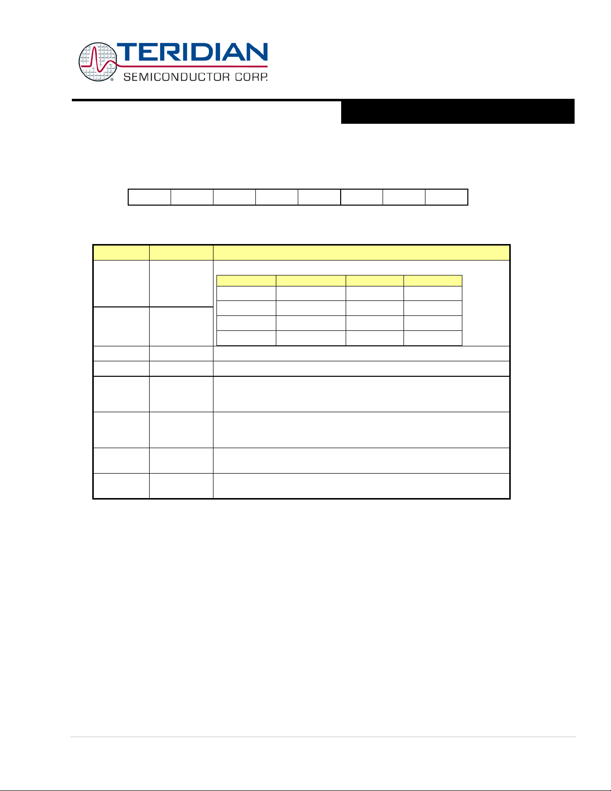
71M6513/71M6513H
3-Phase Energy Meter IC
DATA SHEET
A Maxim Integrated Products Brand
Mode
Description
SM0
SM1
0
N/A 0 0
S0CON
SM1
S0CON.5
SM20
Enables the inter-proc essor c om muni catio n feature.
S0CON
REN0
MPU, depending on the function it performs (parity check, multiprocessor
S0CON.1
TI0
Transmit interrupt f lag, s et by hardware after compl etion of a serial
Serial Interface 1 Control Register (S1CON).
The function of the serial port depends on the setting of the Serial Port Control Register S1CON.
MSB LSB
SM - SM21 REN1 TB81 RB81 TI1 RI1
Table 15: The S1CON register
Bit Symbol Function
S0CON.7 SM0 Thes e two bi ts set t he UART0 mode:
SEPTEMBER 2011
.6
.4
S0CON.3 TB80 The 9th transmitted d ata bit in Modes 2 and 3. Set or cleared by the
S0CON.2 RB80 In Modes 2 and 3 it is the 9th dat a bit received . In Mode 1, if SM20 is 0,
S0CON.0 RI0 Receiv e inter rupt flag, set by hardware after completion of a serial
1 8-bit UART 0 1
2 9-bit UART 1 0
3 9-bit UART 1 1
If set, enables serial reception. Cleared by software to disable reception.
communicatio n etc.)
RB80 is the stop bit. In Mode 0 this bit is not used. Must be cleared by
software
tr ansfer. Must be clea red by softw are.
reception. Must be cleared by software
Table 16: The S0CON Bit Functions
© 2005-2011 Teridian Semiconductor Corporation Page: 25 of 104
Page 26
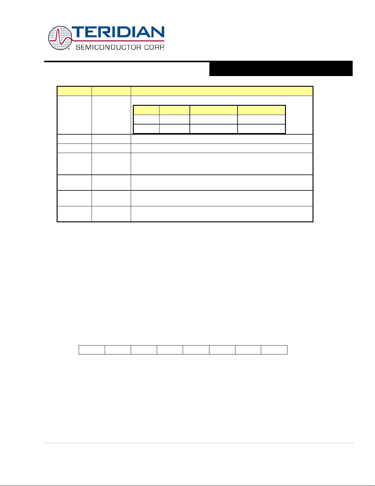
71M6513/71M6513H
3-Phase Energy Meter IC
DATA SHEET
A Maxim Integrated Products Brand
Bit
Symbol
Function
Mode
Description
Baud Rate
S1CON.1
TI1
Transmit interrupt f lag, s et by hardware after compl etion of a serial
S1CON.7 SM Sets the baud rate for UART1
SM
0 A 9-bit UART variable
1 B 8-bit UART variable
S1CON.5 SM21 Enables the inter-processor communi catio n feature.
S1CON.4 REN1 I f set, en ables serial recep tion. Cleared by software to di sable reception.
S1CON.3 TB81 T he 9th transmitted d ata bit in Mode A . Set or cleared by the MPU ,
depending on the function it performs (parity check, multiprocessor
communicatio n etc.)
S1CON.2 RB81 In Modes 2 and 3, it is the 9th dat a bit received . In Mod e B, if SM21 is 0,
RB81 is the sto p bi t. Must be cleared by software
tr ansfer. Must be clea red by softw are.
S1CON.0 RI1 Receiv e inter rupt f lag, s et by hardwar e after compl et ion of a seria l
reception. Must be cleared by software
AUGUST 2011
Table 17: The S1CON Bit Functions
Timers and Counters
The 80515 has two 16-bit timer/counter registers: Timer 0 and Timer 1. These registers can be configured for counter or timer
operations.
In timer mode, the register is incremented every machine cycle meaning that it counts up after every 12 periods of the MPU
clock signal.
In counter mode, the register is incremented when the falling edge is observed at the corresponding input signal T0 or T1 (T0
and T1 are the timer gating inputs derived from certain DIO pins, see the DIO Ports chapter). Since it takes 2 machine cycles
to recognize a 1-to-0 event, the maximum input count rate is 1/2 of the oscillator frequency. There are no restrictions on the
duty cycle, however to ensu re proper recogni tion of 0 or 1 state, an i nput should be stable for at least 1 m achine cycle.
Four operating modes can be selected for Timer 0 and Timer 1. Two Special Function Registers (TMOD and TCON) ar e u s ed
to select the appropriate mode.
Timer/Counter Mode Control register (TMOD):
MSB LSB
GATE C/T M1 M0 GATE C/T M1 M0
Timer 1 Timer 0
Table 18: The TMOD Register
Bits TR1 (TCON.6) and TR0 (TCON.4) in the TCON register (see Table 21 and Table 22) start their associated timers when set.
Page: 26 of 104 © 2005-2011 Teridian Semiconductor Corporation
Page 27
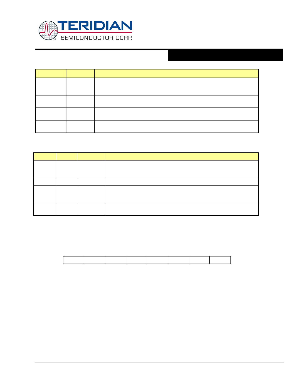
71M6513/71M6513H
3-Phase Energy Meter IC
DATA SHEET
A Maxim Integrated Products Brand
Bit
Symbol
Function
TMOD.5
M1
Selects the mode for Timer/Counter 0 or Timer/Counter 1, as shown in TMOD
M1
M0
Mode
Function
TL0
TL1
1 0 Mode2
8-bit auto-reload Counter/Timer. The reload value is kept in TH0 or TH1,
1 1 Mode3
If Ti mer 1 M1 and M0 bits a re set t o '1', Timer 1 stops. I f Timer 0 M1 and M0
SEPTEMBER 2011
TMOD.7
TMOD.3
TMOD.6
TMOD.2
TMOD.1
TMOD.4
TMOD.0
0 0 Mode 0 13-bit C ounter/Timer with 5 low er bits in the
0 1 Mode 1 16-bit C ounter/Timer.
Note: TL0 is affected by TR0 and gate control bits, and sets TF0 flag on overflow.
TH0 is affected by TR1 bit, and sets TF1 flag on overflow.
Timer/Counter Control Register (TCON)
Gate If set, enables external gate control (p in int0 or int 1 for Cou nter 0 or 1,
respectively). When int0 or int1 is high, and TRX bit is set (see TCON regis ter) , a
counter is incremented every falling edge on t0 or t1 input pin
C/T Selects Timer or Counter operation. When set to 1, a Counter operation is
performed. When cleared to 0, the corresponding reg ister will f uncti on as a Timer.
description.
M0 Selects the mode for Timer/Counter 0 or Timer/Counter 1, as shown in TMOD
description.
Table 19: TMOD Register Bit Description
remaining 8 bits in the TH0 or TH1 regist er (for Timer 0 and Timer 1,
respectively ). The 3 high order bits of TL0 and TL1 are held at zero.
while TL0 or TL1 is incremented every machine cycle. When TL(x )
overfl ows, a value from TH(x) is copied to TL(x).
bits are set to '1', Timer 0 acts as two independent 8-bit Timer/Co unters.
Table 20: Timers/Counters Mode Description
MSB LSB
or
register and the
TF1 TR1 TF0 TR0 IE1 IT1 IE0 IT0
Table 21: The TCON Register
© 2005-2011 Teridian Semiconductor Corporation Page: 27 of 104
Page 28
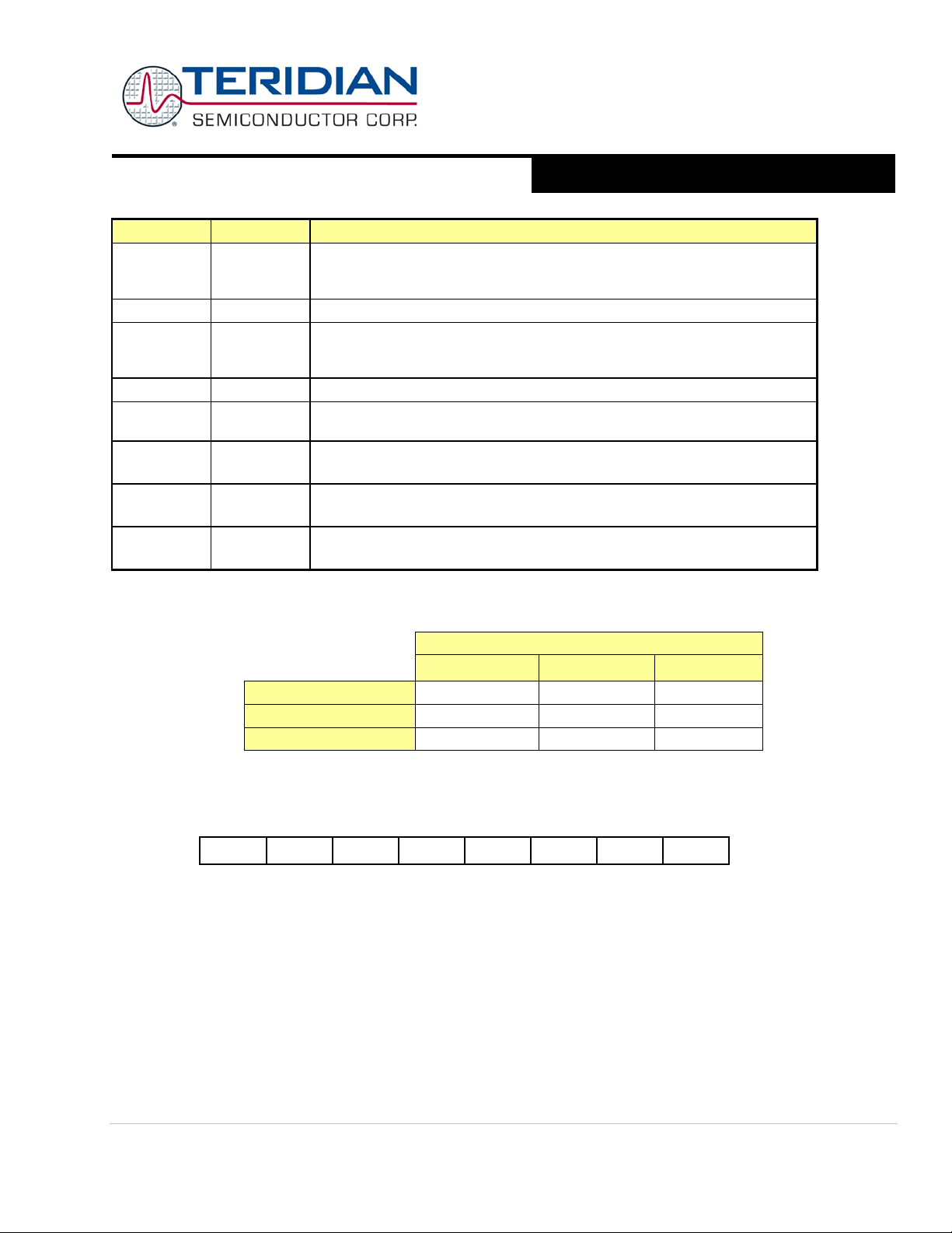
71M6513/71M6513H
3-Phase Energy Meter IC
DATA SHEET
A Maxim Integrated Products Brand
Bit
Symbol
Function
flag set by hardware when Timer 0 overflows. This flag can be
Interrupt 1 type control bit. Selects either the falling edge or low level on input
Interrupt 0 edge flag is set by hardware when the falling edge on external pin
Interrupt 0 type control bit. Selects either the falling edge or low level on input
Timer 0 - mode 0
YES
YES
YES
Timer 0 - mode 2
SMOD
The Timer 1 overflow flag is set by hardware when Timer 1 overflows. This flag
TCON.7 TF1
TCON.6 TR1 Tim er 1 Run control bit. If cleared, Timer 1 stops.
TCON.5 TF0
TCON.4 TR0 Tim er 0 Run control bit. If cleared, Timer 0 stops.
TCON.3 IE1
can be cleared by s oftware and is automati cally cleared when an interrupt is
processed.
Timer 0 overflow
cl eared b y software an d is automaticall y clear ed when a n interrupt is
processed.
Interrupt 1 edge flag is set by hardware when the falling edge on external pin
int1 is observed. Cleared when an interrupt is processed.
AUGUST 2011
TCON.2 IT1
TCON.1 IE0
TCON.0 IT0
Table 23 specifies the combinations of operation modes allowed for ti mer 0 and tim er 1:
Timer 0 - mode 1 YES YES YES
Timer/Counter Mode Control Register ( PCON):
MSB LSB
The SMOD bit in the PCON register doubles the b aud rate w hen set.
pin to cause an interrupt.
int0 is observed. Cleared when an interrupt is processed.
pin to cause interrupt.
Table 22: The TCON Register Bit Functions
Timer 1
Mode 0 Mode 1 Mode 2
Not allowed Not all o wed YES
Table 23: Timer Modes
Table 24: The PCON Register
WD Timer (Software Watchdog Timer)
The software watchdog timer is a 16-bit c ounter th at is in cremen ted onc e every 2 4 or 384 cl ock cy cles. Af ter a res et, th e
watchdog timer is disabled and all registers are set to zero. The watchdog consists of a 16-bit count er (WDT), a reload register
(WDTREL), prescalers (by 2 and by 16), and control logic. Once the watchdog is started, it cannot be stopped unless the
internal reset signal becomes active.
Note: It is recommended to use the hardware watchdog timer instead of the software watchdog timer.
WD Timer Start Procedure: The WD T is start ed b y settin g t h e SWDT flag. When t he WDT reg is ter ent er s th e st at e 0x7C FF ,
an asynchronous WDTS signal will become active. The signal WDTS sets bit 6 in the IP0 register and requests a reset state.
WDTS is cleared either by the reset si gnal or by chan ging the stat e of the WDT.
Page: 28 of 104 © 2005-2011 Teridian Semiconductor Corporation
Page 29
71M6513/71M6513H
3-Phase Energy Meter IC
DATA SHEET
A Maxim Integrated Products Brand
Bit
Symbol
Function
Bit
Symbol
Function
SEPTEMBER 2011
Refreshing the WD Timer: The watchdog timer must be refreshed regularly to prevent the reset request signal from
becoming active. This requirement imposes an obligation on the programmer to issue two instructions. The first instruction
sets WDT and t he second instruction sets SWDT. The maximum delay allowed between setting WDT and SWDT is 12 clock
cycles. If this period has expired and SWDT has not been set, WDT is automatically reset, otherwise the watchdog timer is
reloaded with the content of the WDTREL register and WDT is automatically reset. Since the W DT requires exact t iming,
firmware needs to be designed with special care in order to avoid unwanted WDT resets. Teridian strongly discourages the
use of the software WDT.
Special Function Registers for the WD Timer
Interrupt Enable 0 Register (IEN0):
MSB LSB
EAL WDT ET2 ES0 ET1 EX1 ET0 EX0
Table 25: The IEN0 Register (see also Table 32)
IEN0.6 WDT Watchdog timer refresh flag.
Set to initiat e a refr esh of the watc hdog timer. Must be set direc tly before SWDT is
set to prevent an unintentional r efresh of the w atchdog timer. WDT is reset by
hardware 12 clock cycles after it has been set.
Table 26: The IEN0 Bit Functions (see also Table 32)
Note: The remaining bits in the IEN0 register are not used for watchdog control
Interrupt Enable 1 Register (IEN1):
MSB LSB
EXEN2 SWDT EX6 EX5 EX4 EX3 EX2
Table 27: The IEN1 Register (see also Tables 30/31)
IEN1.6 SWDT Watchdo g t i mer start/ refr esh flag.
Set to acti vate/refresh th e watc hdog timer. When directl y set after setting WDT, a
watchdog timer refresh is performed. Bit SWDT is reset by the hardware 12 clock
cycles after it has been set.
Table 28: The IEN1 Bit Functions (see also Tables 30/31)
Note: The remaining bits in the IEN1 register are not used for watchdog control
© 2005-2011 Teridian Semiconductor Corporation Page: 29 of 104
Page 30
3-Phase Energy Meter IC
DATA SHEET
A Maxim Integrated Products Brand
Bit
Symbol
Function
IP0.6
WDTS
Watchdog timer status flag. Set when the watchdog timer was started. Can be
Bit
Symbol
Function
Interrupt Priority 0 Register (IP0):
MSB LSB
-- WDTS IP0.5 IP0.4 IP0.3 IP0.2 IP0.1 IP0.0
Table 29: The IP0 Register (see also Table 45)
read by softwar e.
Table 30: The IP0 bit Functions (see also Table 45)
Note: The remaining bits in the IP0 register are not used for watchdog control
Watchdog Timer Reload Register (WDTREL):
MSB LSB
7 6 5 4 3 2 1 0
71M6513/71M6513H
AUGUST 2011
Table 31: The WDTREL Register
WDTREL.7 7
WDTREL.6
to
WDTREL.0
The WDTREL register can be loaded and read at any time.
6-0
Prescaler select bit. When set, the watchdog is clocked through an additional
divide-by-16 prescaler
Seven bit reload value for t he high -b yte of the watchdog t imer. This value is
loaded to the WDT when a refresh is triggered by a consecutive setting of bits
WDT and SWDT.
Table 32: The WDTREL Bit Functions
Page: 30 of 104 © 2005-2011 Teridian Semiconductor Corporation
Page 31

71M6513/71M6513H
3-Phase Energy Meter IC
DATA SHEET
A Maxim Integrated Products Brand
SEPTEMBER 2011
Interrupts
The 80515 provides 11 interrupt sources with four priority levels. Each source has its own request flag(s) located in a special
function register (TCON, IRCON, and SCON).
disabled by the enable bits in SFRs IEN0, IEN1, and IEN2.
External interrupts are the interrupts external to the 80515 core, i.e. signals that originate in other parts of the
71M6513/6513H, for example the C E, DIO, RTC EEPROM interface, comparators.
Interrupt Overview: When an interrupt occurs, the MPU will vector to the predetermined address as shown in Table 50. Once
interrupt service has begun, it can be interrupted only by a higher priority interrupt. The interrupt service is terminated by a
return from instruction, "RETI". When a RETI instruction is performed, the processor will return to the instruction that would
have been next when the interrupt occurred.
When the interrupt condition occurs, the processor will also indicate this by setting a flag bit. This bit is set regardless of
whet her th e int er ru pt i s en abl ed or di sa bled . Each int err upt fl ag i s s ampl ed o nc e per ma chi ne c ycl e, then sam pl es ar e po l led
by the har dware. If th e sample indi cates a pendi ng int errupt when t he int errupt is enabled, then the interr upt request flag is set.
On the next instruction cycle, the interrupt will be acknowledged by hardwar e forcing an LCALL to the appropriate vector
address, if the following conditions are met:
• No interrupt of equal or high er priority is alr eady in progress.
• An instruction is currently being executed and is not completed.
Each interrupt requested by the corresponding flag can be individually enabled or
• The instructi on in progress is not RETI or any wr i te access to the register s IEN0, IEN1, IEN2, IP0 or IP1.
Interrupt response will require a varying amount of time depending on the state of the MPU when the interrupt occurs. If the
MPU is performing an interrupt service with equal or greater priority, the new interrupt will not be invoked. In other cases, the
response time depends on the current instruction. The fastest possible response to an interrupt is 7 machine cycles. This
includes one machine cycle for detecting the interrupt and six cycles to perform the LCALL.
© 2005-2011 Teridian Semiconductor Corporation Page: 31 of 104
Page 32
3-Phase Energy Meter IC
DATA SHEET
A Maxim Integrated Products Brand
Special Function Registers for Interrupts:
IEN0
EAL
EAL
IEN0.6
WDT
Not used for interrupt control
Bit
Symbol
Function
IEN1.6
SWDT
Not used for interrupt control
Interrupt Enable 0 register (IE0)
MSB LSB
EAL WDT ES0 ET1 EX1 ET0 EX0
Bit Symbol Function
71M6513/71M6513H
AUGUST 2011
Table 33: The IEN0 Register
.7
IEN0.5 -
IEN0.4 ES0 ES0=0 – disable s er ial c hannel 0 interrupt
IEN0.3 ET1 ET1=0 – disable timer 1 overflow i nterr upt
IEN0.2 EX1 EX1=0 – dis able external int er rupt 1
IEN0.1 ET0 ET0=0 – disable timer 0 overflow interrupt
IEN0.0 EX0 EX0=0 – dis able external int er rupt 0
Interrupt Enable 1 Register (IEN1)
MSB LSB
IEN1.7 -
IEN1.5 EX6 EX6=0 – disable external interrupt 6
IEN1.4 EX5 EX5=0 – disable external interrupt 5
IEN1.3 EX4 EX4=0 – disable external interrupt 4
IEN1.2 EX3 EX3=0 – disable external interrupt 3
IEN1.1 EX2 EX2=0 – disable external interrupt 2
IEN1.0 -
=0 – disable al l interrupts
Table 34: The IEN0 Bit Functions
SWDT EX6 EX5 EX4 EX3 EX2
Table 35: The IEN1 Register
Page: 32 of 104 © 2005-2011 Teridian Semiconductor Corporation
Table 36: The IEN1 Bit Functions
Page 33
3-Phase Energy Meter IC
DATA SHEET
A Maxim Integrated Products Brand
TCON.7
TF1
Timer 1 overflow flag
Interrupt Enable 2 register (IE2)
MSB LSB
- - - - - - - ES1
Table 37: The IEN2 Register
Bit Symbol Function
IEN2.0 ES1 ES1=0 – dis able ser ial c hannel 1 interrupt
Table 38: The IEN2 Bit Functions
Timer/Counter Control register (TCON)
MSB LSB
TF1 TR1 TF0 TR0 IE1 IT1 IE0 IT0
71M6513/71M6513H
SEPTEMBER 2011
Table 39: The TCON Register
Bit Symbol Function
TCON.6 TR1 Not used for interrupt control
TCON.5 TF0 Timer 0 overfl ow flag
TCON.4 TR0 Not used for interrupt control
TCON.3 IE1 External interrupt 1 flag
TCON.2 IT1 External interrupt 1 type control bit
TCON.1 IE0 External interrupt 0 flag
TCON.0 IT0 External interrupt 0 type control bit
Table 40: The TCON Bit Functions
Interrupt Request register (IRCON)
MSB LSB
EX6 IEX5 IEX4 IEX3 IEX2
Table 41: The IRCON Register
© 2005-2011 Teridian Semiconductor Corporation Page: 33 of 104
Page 34
71M6513/71M6513H
3-Phase Energy Meter IC
DATA SHEET
A Maxim Integrated Products Brand
IRCON.3
IEX4
IRCON.2
IEX3
IRCON.1
IEX2
External interrupt 2 edge flag
5
EEPROM busy
falling
automatic
AUGUST 2011
Bit Symbol Function
IRCON.7 -
IRCON.6 -
IRCON.5 IEX6 External interrupt 6 edge flag
IRCON.4 IEX5 External interrupt 5 edge flag
External interrupt 4 edge flag
External interrup t 3 edge flag
IRCON.0 -
Table 42: The IRCON Bit Functions
Note: Only TF0 and TF1 (timer 0 and timer 1 overflow flag) will be automatically cleared by hardware when the service routine
is called (Signals T0ACK and T1ACK – port ISR – act ive hi gh when the service routi ne is cal led).
External Interrup t s
The external interrupts are connected as shown in Table 43. The polarity of interrupts 2 and 3 is programmable in the MPU.
Interrupts 2 and 3 should be programmed for falling sensitivity. The generic 8051 MPU literature states that interrupts 4
through 6 are defined as rising edge sensitive. Thus, the hardware signals attached to interrupts 5 and 6 are inver ted to
achieve the edge polarity shown in Table 43.
SFR (special function register) enable bits must be set to permit any of these interrupts to occur. Likewise, each interrupt has
its own flag bit that is set by the interrupt hardware and is reset automatically by the MPU interrupt handler (0 through 5).
XFER_BUSY and RTC_1SEC, which are OR-ed together, have their own enable and flag bits in addition to the interrupt 6
enable and flag bits (see Table 44), and t hese interrupts m ust be cleared by the MPU sof tware.
External
Interrupt
0 Digital I/O High Priority see DIO_Rx automatic
1 Digital I/O Low Priority see DIO_Rx automatic
2 Comparator 2 or 3 falling automatic
3 CE_BUSY falling automatic
4 Comparator 2 or 3 rising automatic
6 XFER_BUSY OR RTC_1SEC falling manual
Interrupt 6 is edge-sensitive. Th e RTC_1 SEC int errupt from t he RTC a nd the X FER_B USY i nterr upt fr om the CE are com bined using a logic OR function and the result is routed into interrupt 6. Therefore, both flags must be cleared at least once
during i nitial izat ion, and both flags m ust al w ays be cleared befo re exit ing th e inter rupt servic e routine (IS R) for i nterr upt 6.
Note 1: If clearing of both flags is not performed, then no edge can occur to t ri gger int errupt 6 later r esulting in the I SR for the
XFER_BUSY ceasing to run.
Note 2: Clearing both flags reliably requires some care. Either flag can be set by hardware while interrupt 6 code is running on
behalf of the other interrupt. In this situation, the unprocessed interrupt can create a lockout condition similar to the one in note
1. To preven t this lockout on e m ust al w ays process both in terru pt flag s in th e same service r outi ne.
Page: 34 of 104 © 2005-2011 Teridian Semiconductor Corporation
Connection Polarity Flag Reset
Table 43: Extern a l MPU Interrupts
Page 35
71M6513/71M6513H
3-Phase Energy Meter IC
DATA SHEET
A Maxim Integrated Products Brand
Enable Bit
Description
Flag Bit
Description
EX1
Enable external interrupt 1
IE1
External interrupt 1 flag
EX3
Enable external interrupt 3
IEX3
External interrupt 3 flag
EX4
IEX4
Group
SEPTEMBER 2011
Note 3: After a reset fr om an in-circu i t emul ator, the IE_XFER flag may not be cleared because the CE may continue to run.
The flags for the RTC_1SEC and the XFER_BUSY inte rrupts are located in the WDI SFR (address 0xE8).
EX0 Enable external interrupt 0 IE0 External interrupt 0 flag
EX2 Enable external interrupt 2 IEX2 External interrupt 2 flag
Enable external interrupt 4
EX5 Enable external interrupt 5 IEX5 External interrupt 5 flag
EX6 Enable external interrupt 6 IEX6 External interrupt 6 flag
EX_XFER Enable XFER_BUSY interrupt IE_XFER XFER_BUSY i nterrupt flag
EX_RTC Enable RTC_1SEC interrupt IE_RTC RTC_1SEC interrupt flag
Table 44: Control Bits for External Interrupts
External interrupt 4 flag
Interrupt Prio rity Level Structure
All interrupt sources are combined in groups, as shown in Table 45:
0 External inter rupt 0 Serial channel 1 in terr upt
1 Timer 0 interrupt - External interrupt 2
2 External inter rupt 1 - External interrupt 3
3 Timer 1 interrupt - External interrupt 4
4 Seri al channel 0 interrupt - External interrupt 5
5 - - External interrupt 6
Table 45: Priority Level Groups
Each group of interrupt sources can be programmed individually to one of four priority levels by setti ng or clearing one bit in
the special function register IP0 and one in IP1.
polling sequence as per Table 49 det er min es whic h r equest is ser viced f irst.
IEN enable bits must be set to permit any of these interrupts to occur. Likewise, each interrupt has its own flag bit that is set by
the i n ter ru pt har dware and is reset automatically by the MPU interrupt handler (0 t hrough 5). XFER_BUSY and RTC_1SEC,
which are OR-ed together, have their own enable and flag bits in addition to the interrupt 6 enable and flag bits (see Table 44),
and these interrupts must be cleared by the MPU software.
An o verview of the inter rupt s t ructure is shown i n Figure 7.
I f req ues ts of t he s am e prio rit y l evel ar e r ecei ved sim ult an eou sly , a n inter na l
© 2005-2011 Teridian Semiconductor Corporation Page: 35 of 104
Page 36
3-Phase Energy Meter IC
DATA SHEET
A Maxim Integrated Products Brand
Interrupt Priority 0 Register (IP0)
IP1.5
IP1.4
IP1.3
IP1.2
IP1.1
IP1.0
0
0
Level0 (lowest)
External interrupt 3
MSB LSB
-- WDTS IP0.5 IP0.4 IP0.3 IP0.2 IP0.1 IP0.0
Interrupt Priority 1 Register (IP1)
MSB LSB
- -
71M6513/71M6513H
AUGUST 2011
Table 46: The IP0 Register:
Note: WDTS is not used for interrupt controls
Table 47: The IP1 Register:
IP1.x IP0.x
0 1 Level1
1 0 Level2
1 1 Level3 (highest)
Table 48: Priority Levels
External interrupt 0
Serial channel 1 interrupt
Timer 0 interrupt
External interrupt 2
External interrupt 1
Timer 1 interrupt
External interrupt 4
Serial channel 0 interrupt
External interrupt 5
External interrupt 6
Priority Level
Polling sequence
Page: 36 of 104 © 2005-2011 Teridian Semiconductor Corporation
Table 49: Interrupt Polling Sequence
Page 37
3-Phase Energy Meter IC
DATA SHEET
A Maxim Integrated Products Brand
TF0
IE1
External interrupt 1
0x0013
IEX3
IEX4
IEX5
External interrupt 5
0x0063
Interrupt Sou rces and Vectors
Table 50 shows the interrupts with their associated flags and vector addresses.
Interrupt Request Flag Description Interrupt Vector Address
IE0 External interrupt 0 0x0003
Timer 0 interrupt 0x000B
TF1 Timer 1 interrupt 0x001B
RI0/TI0 Serial channel 0 interrupt 0x0023
RI1/TI1 Serial c hannel 1 interrupt 0x0083
IEX2 External interrupt 2 0x004B
External interrupt 3 0x0053
External interrupt 4 0x005B
IEX6 External interrupt 6 0x006B
71M6513/71M6513H
SEPTEMBER 2011
Table 50: Interrupt Vectors
© 2005-2011 Teridian Semiconductor Corporation Page: 37 of 104
Page 38
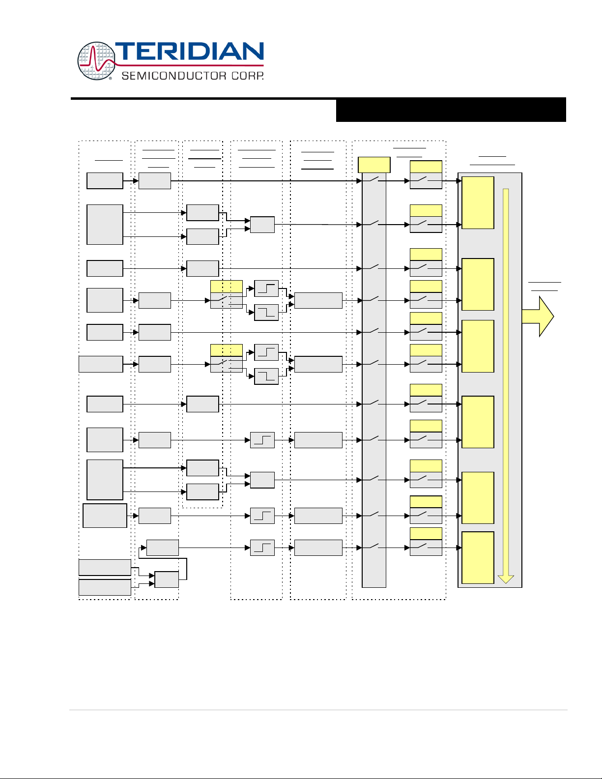
71M6513/71M6513H
3-Phase Energy Meter IC
DATA SHEET
A Maxim Integrated Products Brand
IE0
External
Interrupt
Flags
RI1
TI1
Internal
Interrupt
Flags
Source
>=1
TF0
INT2
IE1
INT3
TF1
INT4
RI0
TI0
>=1
INT5
INT6
>=1
IRCON.1
I2FR
IRCON.2
I3FR
IRCON.3
IRCON.4
IRCON.5
IEN0.7
IP1.0/
IP0.0
IP1.1/
IP0.1
IP1.2/
IP0.2
IP1.3/
IP0.3
IP1.4/
IP0.4
IP1.5/
IP0.5
Interrupt
Control
Register
Priority
Assignment
Interrupt
Vector
Polling Sequence
Interrupt
Enable
Logic and
Polarity
Selection
DIO
UART1
(optical)
Timer 0
Compar-
ators
Compar-
ators
DIO
Timer 1
CE_BUSY
UART0
EEPROM/
I2C
XFER_BUSY
RTC_1S
IEN0.0
IEN2.0
IEN0.1
IEN1.1
IEN0.2
IEN1.2
IEN0.3
IEN1.3
IEN0.4
IEN1.4
IEN1.5
AUGUST 2011
Page: 38 of 104 © 2005-2011 Teridian Semiconductor Corporation
Figure 7: Interrupt Structure
Page 39
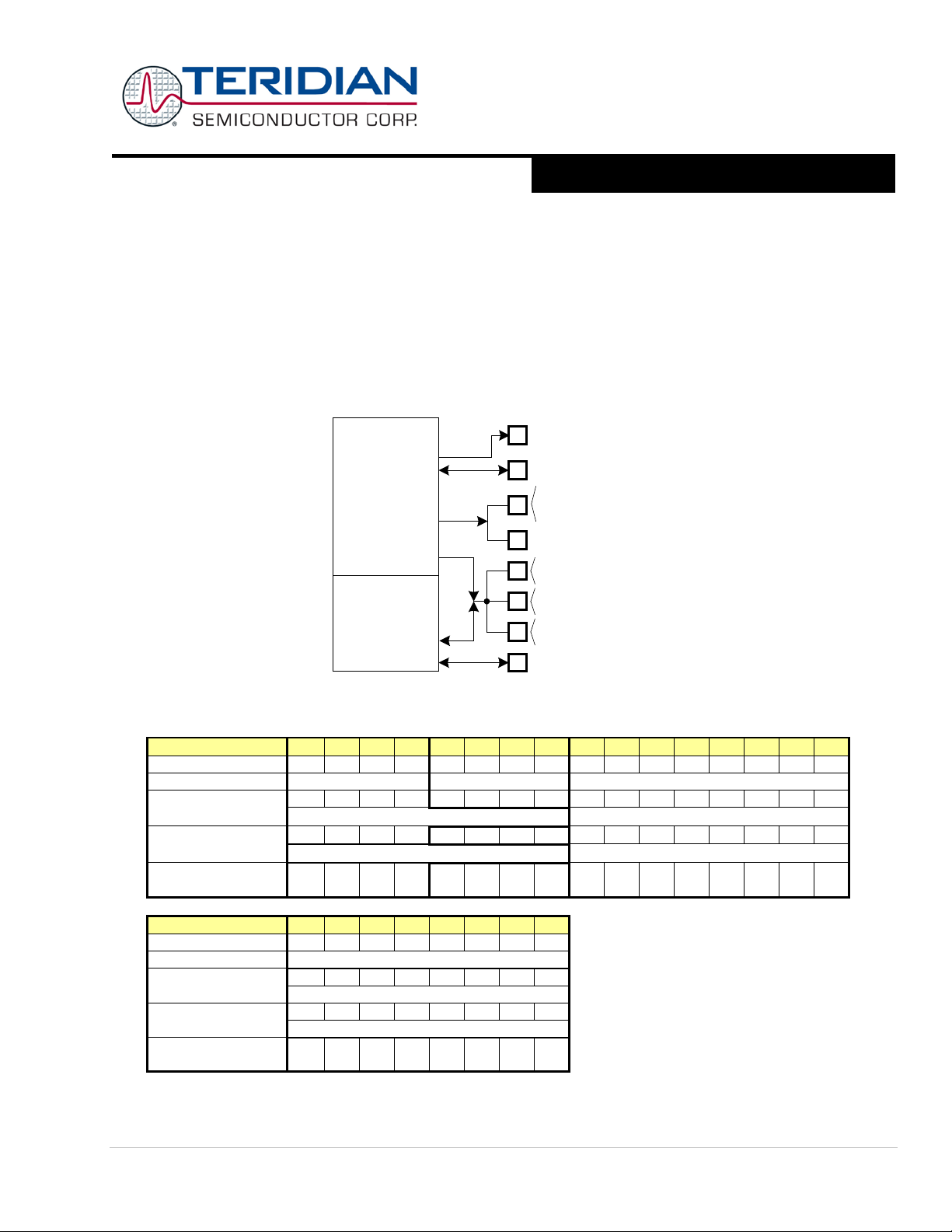
71M6513/71M6513H
3-Phase Energy Meter IC
DATA SHEET
A Maxim Integrated Products Brand
DIO 0 1 2 3 4 5 6 7 8 9
10
11
12
13
14
15
Pin number
18
19
20
21
60
61
62
63
67
68
69
70
98
99
30
31
Pin type
DIO
Multi-use
Multi-use
0 1 2 3 4 5 6 7 0 1 2 3 4 5 6
7
DIO0=P0 (SFR 0x80)
DIO1=P1 (SFR 0x90)
Directi on Register
bit
--
--
--
-- 4 5 6 7 0 1 2 3 4 5 6 7
DIO_DIR0 (SFR 0xA2)
DIO_DIR1 (SFR 0x91)
Internal Resources
Configurable
DIO
16
17
18
19
20
21
22
23
Pin number
34
16
17
64
65
66
--
--
Pin type
Multi-use
0 1 2 3 4 5 --
--
DIO2=P2 (SFR 0xA0)
Directi on Register
bit
0 1 2 3 4 5 --
--
DIO_DIR2 (SFR 0xA1)
Internal Resources
Configurable
COM0..3
LCD DISPLAY
DRIVER
DIGITAL I/O
LCD_EN
LCD_CLK
LCD_MODE
DIO_GP
SEG20..23
DIO_0..3
SEG28/DIO8 ..
SEG31/DIO11
LCD_NUM
DIO_OUT
DIO_IN
LCD_NUM
PULSEV/W
SEG24/DIO4 ..
SEG27/DIO7
SEG32/DIO12 ..
SEG41/DIO21
SEG0..2, SEG3/SCLK,
SEG4/SSDATA,
SEG5/SFR, SEG7..19
DIO_EEX
SEG6/SRDY
SEPTEMBER 2011
On-Chip Resources
DIO Ports
The 71M6513/6513H includes up to 22 pins of general purpose digital I/O. 18 of these pins are dual function and can
alternatively be us ed as LCD dr iver s. Figure 8 shows a block diagram of th e D I O section.
On reset or power-up, all DIO pins are inputs until they are configured for the desired direction. The pins are configured and
controlled by the DIO and DIO_DIR reg is ter s ( SFR s) an d by the f iv e bit s of th e I/O reg is ter LCD_NUM (0x2020[4:0]). See the
description for LCD_NUM in the I/O RAM Section for a table listing the available segment pins versus DIO pins, depending on
the s election for LCD_NUM. Generally, increasing the value for LCD_NUM will configure an increasing number of general
purpose pins to be LCD segment pins, starting at the higher pin numbers.
Data Register bit
Y Y Y Y Y Y Y Y Y Y Y Y N N N N
Data Register bit
© 2005-2011 Teridian Semiconductor Corporation Page: 39 of 104
Table 51: Data Registers, Direction Registers and Internal Resources for DIO Pin Groups
N N N N N N -- --
Figure 8: DIO Ports Block Diagram
Page 40
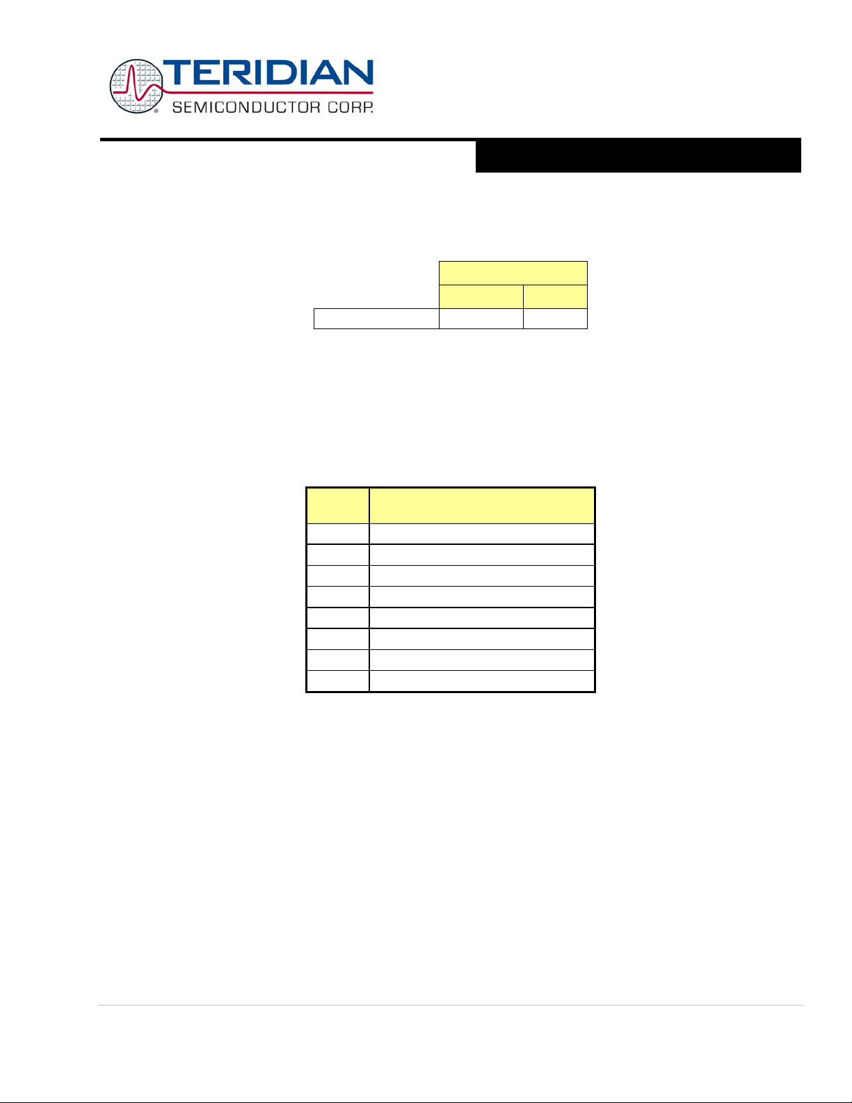
71M6513/71M6513H
3-Phase Energy Meter IC
DATA SHEET
A Maxim Integrated Products Brand
6
High priority I/O interrupt (INT0 falling)
AUGUST 2011
Each pin declared as DIO can be configured independently as an input or output with the bits of the DIO_DIRn registers. Table
51 lists the direction registers and configurability associated with each group of DIO pins. Table 52 shows the configuration for
a DIO pin through its associated bit in its DIO_DIR register.
DIO_DIR bit
0 1
DIO Pin Function input output
Table 52: DIO_DIR Contro l Bit
Values read from and written into the DIO ports use the data registers P0, P1 and P2.
A 3-bit configuration word, I/O RAM register, DIO_Rx (0x2009[2:0] through 0x200E[6:4]) can be used for certai n pins, when
configured as DIO, to individually assign an internal resource such as an interrupt or a timer control (see Table 51 for DIO pins
available for this option). This way, DIO pins can be tracked even if they are configur ed a s o utp uts . Th is fea tur e i s us ef ul f or
pulse counting. The control resources selectable for the DIO pins are listed in Table 53. If more than one input is connected to
the same resource, the resources are combine d using a logical OR.
DIO_R
Value
0 NONE
1 Reserved
2 T0 (counter0 clock)
3 T1 (counter1 clock)
4 High priority I/O interrupt (INT0 rising)
5 L ow priorit y I/O interrupt (INT1 rising)
7 L ow priorit y I/O interrupt (INT1 fal l ing)
Table 53: Selectable Controls using the DIO_DIR Bits
Additionally, if DIO6 and DIO7 are declared outputs, they can be configured as dedicated pulse outputs (WPULSE = DIO6,
VARPULSE = DIO7) using t he I/O RAM regist ers DIO_PW (0x2008[2]) and DIO_PV (0x2008[3]). In this case, DIO6 and DIO7
are under CE control. DIO4 and DIO5 can be configured to implement the EEPROM Interface by setting the I/O RAM register
DIO_EEX (0x2008[4]).
Resource Selected for DIO Pin
Page: 40 of 104 © 2005-2011 Teridian Semiconductor Corporation
Page 41
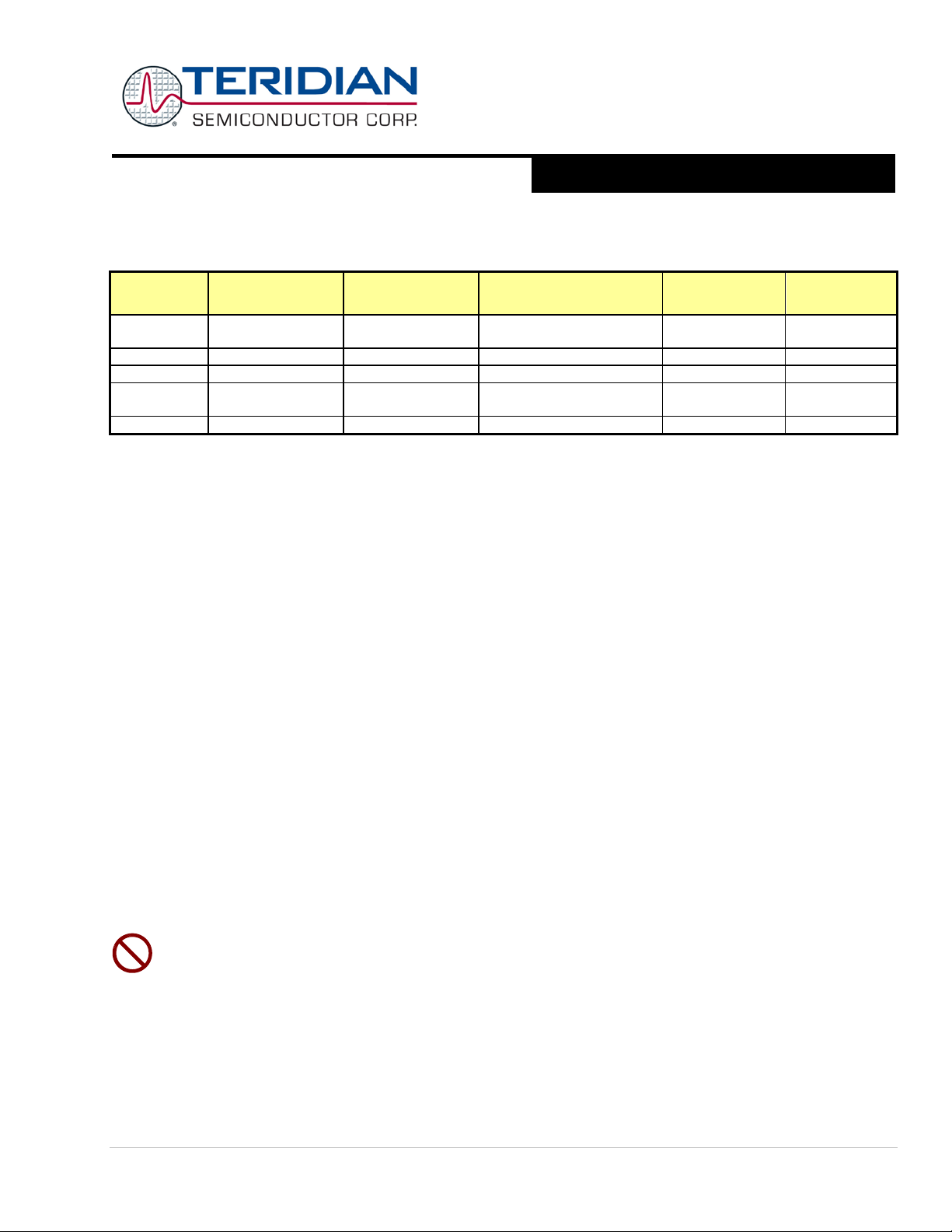
3-Phase Energy Meter IC
DATA SHEET
A Maxim Integrated Products Brand
Program and non-volatile
data
0000-07FF
Static RAM
Battery-buffered
MPU data RAM
0
2KB
1000-13FF
Static RAM
Volatile
CE data
5
1KB
Configuration RAM
(I/O RAM)
3000-3FFF
Static RAM
Volatile
CE Program code
5
4KB
Physical Memory
Data bus address space is allocated to on-chip memory as shown in Table 54.
71M6513/71M6513H
SEPTEMBER 2011
Address
(hex)
0000-FFFF Flash Memory Non-volatile
2000-20FF Static RAM Volatile
Flash Memory: The 71M6513 includes 64KB of on-chip flash me mory. The flash memory is intended to primarily conta in MPU
program code. In a typical application, it also contains images of the CE program code, CE coefficients, MPU RAM, and I/O
RAM. On power-up, before enabling the CE, the MPU must copy these images to their respective memory locations.
The I /O RAM bi t r egi st er FLASH66Z defines the pulse width for accessing flash memory. To minimize supply current draw,
this bit should be set to 1.
Flash erasure is initiated by writing a specific data pattern to specific SFR registers in the proper sequence. These special
pattern/sequence requirements prevent inadvertent erasure of the flash memory.
The mass er ase seq uence i s:
1. Write 1 to t he FLSH_MEEN bit (SF R addres s 0xB2[1].
2. Write pattern 0xAA to FLSH_ERASE (SFR address 0x94)
Note: The mass erase cycle can only be initiated when the ICE port is enabled.
The page erase sequence is:
1. Write the page address to FLSH_PGADR (SFR address 0xB7[7:1]
2. Write pattern 0x55 to FLSH_ERASE (SFR address 0x94)
Writing to flash memory:
The MPU may write to the flash m emory for non-volatile data storage or when implementing a boot-loader. The I/O RAM
register FLSH_PWE (flash program write enable, SFR B2[0]) differentiates 80515 data store instructions (MOVX@DPTR,A)
between Flash and XRAM writes. Befo re set ting FLSH_PWE, all interrupts need to be disabled by setting EAL =1. After the
write operation, FLSH_PWE must be cleared.
The original state of a flash byte is 0xFF ( all bi ts ar e 1) . Ov erwriti ng programmed flash cells with a different value usually requires that the cell is erased first. Since cells cannot be erased individually, the page has to be copied to RAM, followed by a
page erase. After this, the page can be updated in RAM and then written back to the flash memory.
Writing to flash locations will affect the corresponding XRAM cells, i.e. 0x2000 to 0x20FF (I/O RAM), 0x0000 to
0x07FF (MPU RAM), plus CE DRAM and CE PRAM. It is critical to maintain the integrity of the cells 0x2000…0x2007
as a minimum (where important system settings are stored) during the flash-write operation. This can be achieved by
excluding the critical addresses from the write operation.
MPU RAM: The 71M6513 includes 2KB of static RAM memory on-chip (XRAM), which are backed-up by the battery plus 256-
bytes of internal RAM in the MPU core. The 2KB of static RAM are used for data storage during normal MPU operations.
CE DRAM: The CE DR AM is the data memory of the CE. The MPU can re ad and write the CE DRAM as the primary means of
data communication between the tw o processor s.
CE PRAM: The CE PRAM is the program memory of the CE. The CE PRAM has to be loaded with CE code before the CE
starts operating. CE PRAM cannot be accessed by the MPU when the CE is running.
Memory
Technology
Mem ory Type Typical Usage
Table 54: MPU Data Memory Map
Wait States
(at 5MHz)
0 64KB
0 256
Mem ory Si ze
(bytes)
© 2005-2011 Teridian Semiconductor Corporation Page: 41 of 104
Page 42
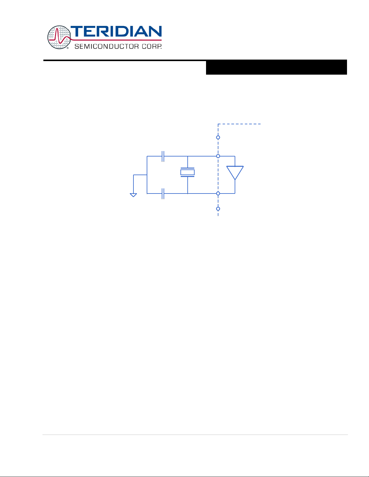
71M6513/71M6513H
3-Phase Energy Meter IC
DATA SHEET
A Maxim Integrated Products Brand
crystal
XOUT
XIN
71M651X
AUGUST 2011
Oscillator
The oscillator drives a standard 32.768kHz watch crystal (see Figure 9). Crystals of this type are accurate and do not require a
high current oscillator circuit. The oscillator in the 71M6513 Power Meter IC has been designed specifically to handle watch
crystals and is compatible with their high impedance and limited power handling capability. The oscillator power dissipation is
very low to maximize the lifetime of any battery backup device attached to the VBAT pin.
Figure 9: Oscillator Circuit
The oscillator should be placed as close as possible to the IC, and vias should be avoided.
An external resistor across the crystal must not be added.
Real-Time Clock (RTC)
The RT C is dr iven d irect ly by t he cry stal os cill ator. In the ab sence o f th e 3.3V s upply, the RTC is power ed by t he exter nal
battery (VBAT pin). The RTC consists of a counter chain and output registers. The counter chain consists of se conds, minute s,
hours, day of week, day of month, month, and year. The RTC is capable of processing leap years. Each counter has its own
output register. Whenever the MPU reads the seconds register, all other output registers are automatically updated. Since the
RTC clock is not coherent to the MPU clock, the MPU must read the seconds register until two consecutive reads are the
sam e (r equ ir es ei t her 2 or 3 rea ds) . At thi s poi nt, all RT C ou tp ut reg ist er s wi ll hav e t he c or rec t t im e. Reg ar dl ess of th e MPU
clock speed, RTC reads require one wait state.
The RTC interrupt must be enabled using t he I/O RAM register EX_RTC (address 0x2002[1]). RTC time is set by writing to the
I/O RAM registers RTC_SEC, RTC_MIN, through RTC_YR. Each byte written to RTC must be delayed at least 3 CK32 cycles
from any previous byte written to RTC.
Two t im e correc tion bits, the I/ O RAM r egis ters RTC_DEC_SEC (0x201C[1]) and RTC_INC_SEC (0x201C[0]) are provided to
adjust the RTC time. A pulse on one of these bits causes the time to be decremented or incremented by an additional second
at the next update of the RTC_SEC register. Thus, if the crystal temperature coefficient is known, the MPU firmware can
integrate tem perature and c orrect the RT C tim e as necessary as discussed in temperature compensation.
Comparators (V 2, V3)
The 71M6513/6513H includes two programmable comparators that are connected to the V2 and V3 pins. The I/O RAM
register COMP_INT (0x2003[4:3]) al l o ws th e u ser t o d et er m i ne i f compar at ors 2 and 3 will trigger an interrupt to the MPU. The
output of each comparator is available in the COMPSTAT register. VBIAS is used as the threshold, and built-in hysteresis
prevents each comparator from repeatedly responding to low-amplitude noise.
Comparators 2 and 3 can be used for early warning of power faults, or for monitoring of battery or other DC voltages. If they
are both selected to interrupt the MPU, their outputs will be XORed together. The voltage at V3 is also available to the ADC in
the AFE, but the comparator should not be u sed when V3 is used for analog measur ements .
Comparator 1 is part of the power fault circuitry (see section V1 Pin) and cannot be programmed.
Page: 42 of 104 © 2005-2011 Teridian Semiconductor Corporation
Page 43
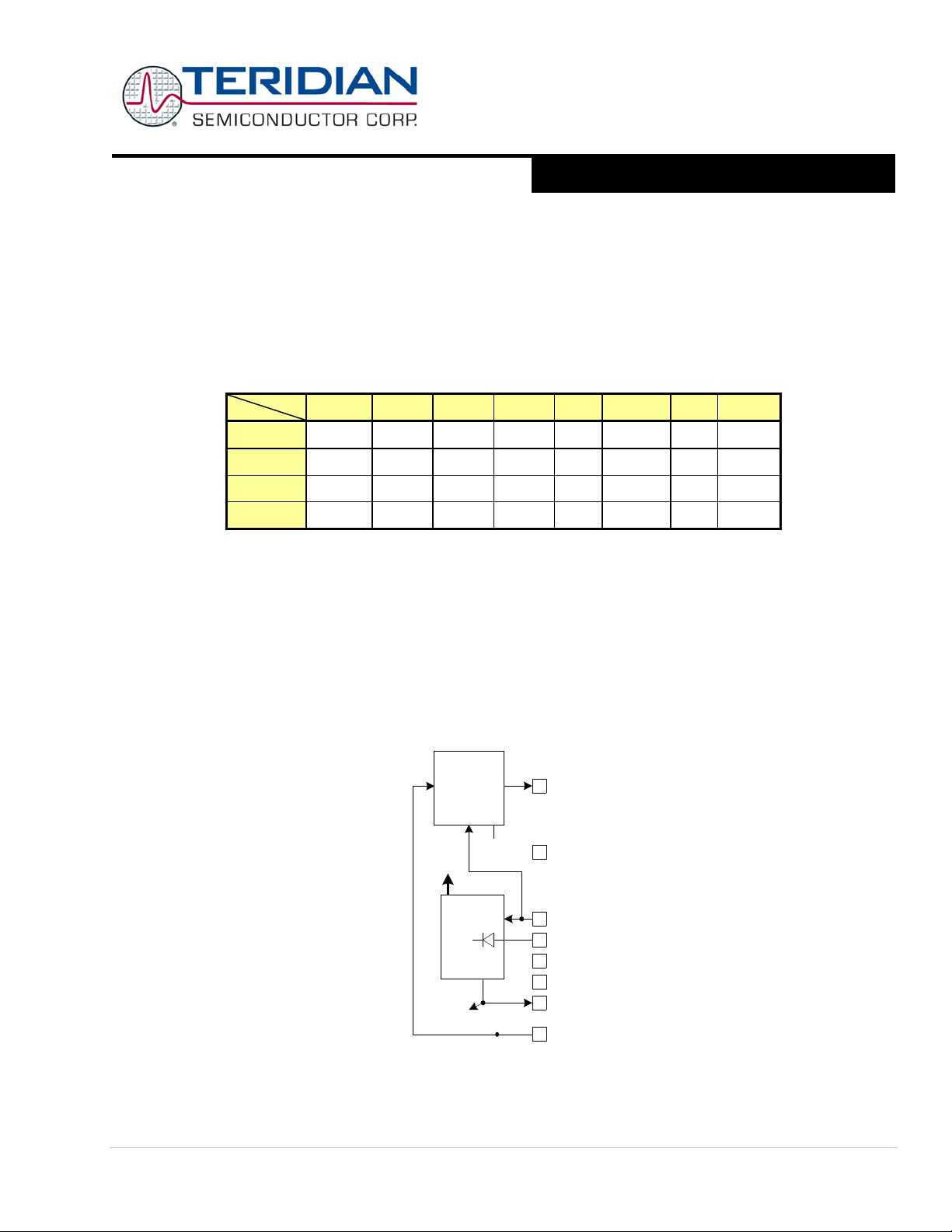
71M6513/71M6513H
3-Phase Energy Meter IC
DATA SHEET
A Maxim Integrated Products Brand
P2
P6
P10
P14
...
P110
...
P166
P3
P7
P11
P15
...
P111
...
P167
GNDD
V3P3D
VBAT
VOLT
REG
0.1V
V2P5
VLCD
VDRV
VOLTAGE
BOOST
LCD_BSTEN
LCD_IBST
GNDD
GNDD
GNDD
V2P5
V3P3D
V2P5NV
SEPTEMBER 2011
LCD Drivers
The 71M6513 contains 24 dedicated LCD segment drivers and 18 multi-purpose pins which may be configured as additional
LCD s eg m en t d ri v er s ( s ee I / O R AM r egi s t er LCD_NUM). The 71M6513/6513H is capable of driving between 96 to 168 pixels
of LCD display with 25% duty cycle. At seven segments per digit, the LCD can be designed for 13 to 24 digits for display.
Since each pixel is addressed individually, the LCD display can be a combination of alphanumeric digits and enunciator
symbols. The information to be displayed is written into the lower four bits of I/O RAM registers LCD_SEG0 through
LCD_SEG41. Bit 0 corresp onds to the segment s elect ed when C OM0 pin is acti ve while bit 1 is allo cated to COM1.
The LCD driver circuitry is grouped int o 4 common outputs (COM0 to COM3) and up to 42 segment outputs (see Table 55).
The typical LCD map is shown below.
SEG0 SEG1 SEG2 SEG3 … SEG27 … SEG41
COM0
COM1
COM2
COM3
Note: P0 , P1, … R epresen t the pixel/segm ent numbers on the LCD .
A charge pump suitable for driving VLCD is included on-chip. This circuit creates 5V from the 3.3V supply. A contrast DAC is
provided that permits the LCD full-scale voltage to be adjusted between VLCD and 70% of VLCD. The LCD_NUM register
defines the number of dual purpose pins used for LCD segment interface.
P0 P4 P8 P12 ... P108 ... P164
P1 P5 P9 P13 … P109 ... P165
Table 55: Liquid Crystal Display Segment Table (Typical)
LCD Voltage Boost Circui t ry
A voltage boost circuit may be used to generate 5V from the 3.3V supply to support low-power 5V devices, such as LCDs.
Figure 10 shows a block diagram of the voltage boost circuitry including the voltage regulators for V2P5 and V2P5NV. When
activated using the I/O RAM register LCD_BSTEN (0x2020[7]), the boost circuitry provides an AC voltage at the VDRV output
pin (see the Applications section for details).
© 2005-2011 Teridian Semiconductor Corporation Page: 43 of 104
Figure 10: LCD Voltage Boost Circuitry
Page 44

71M6513/71M6513H
3-Phase Energy Meter IC
DATA SHEET
A Maxim Integrated Products Brand
AUGUST 2011
UART (UART0) and Optical Port ( UART1)
The 71M6513/6513H includes an interface to implement an IR or optical port. The pin OPT_TX is designed to directly drive an
external LED for transmitting data on an optical link (low-active). The pin OPT_RX, also low-active, is designed to sense the
inp ut fr om an extern al phot o det ector used as th e rec eiver for the op tic al li nk. T hese two pins are connected to a dedicated
UART port. OPT_TX can be tristated if it is desired to multiplex another I/O pin to the OPT_TX output. The control bit for the
OPT_TX output is the I/O RAM register OPT_TXDIS (0x2008[5]).
Hardware Reset Mechani sms
Several conditions will cause a hardware reset of the 71M6513/6513H:
• Voltage at the RESETZ pin low
• Voltage at the E_RST pin low
• Voltage a t the V1 pin below reset threshold (VBIAS)
• The crystal frequency monitor detected a crystal malfunction
• Hardware Watchdog timer
Reset Pin (RESETZ)
When the RESETZ pin is pulled low (or when V1 < VBIAS), all digital activity in the chip stops while analog circuits are still
active. The oscillator and RTC module continue to run. Additionally, all I/O RAM bits are cleared.
Hardware Watchdog Timer
In addition to the basic software watchdog timer included in the 80515 MPU, an independent, robust, fixed-duration, hardware
watchdog timer (WDT) is included in the 71M6513/6513H. This timer will reset the MPU if it is not refreshed periodically, and
can be used to recover the MPU in situations where program control is lost.
The watchdog timer uses the RTC crystal oscillator as its time base and requires a reset under MPU program control at least
every 1.5 seconds. When the WDT overflow occ ur s, t h e MPU i s momenta ri l y res et a s i f RE SE T Z w er e pu l l ed l ow for h al f of a
crystal oscillator cycle. Thus, after 4100 cycles of CK32 (32768Hz clock) , the MPU program will be launched from address 00.
An I/O RAM register status bit, WD_OVF (0x2002[2]), is set when WDT overflow occurs. This bit is powered by the VBAT
pin and can be read by the MPU to determine if the part is initializing after a WDT overflow event or after a power up. After
reading this bi t, MPU firmware must c lear WD_OVF. The WD_OVF bit is also clea red by the RES ETZ pin .
The watchdog timer also includes an oscillator check. If the crystal oscillator stops or slows down, WD_OVF is set and a
system r eset wil l be perform ed when t he crystal oscill ator r esumes .
Ther e is no int er nal di git al state that deactivates the WDT. For debug purposes, however, the WDT can be disabled by tying
the V1 pin to V3P3 (see Figure 11 and WD Disable Threshold [V1-V3P3A] in the Comparator Section of the Electrical
Specifications). Of course, this also deactivates the power fault detection implemented with V1. Since there is no way in firmware to disable the crystal oscillator or the WDT, it is guaranteed that whatever stat e the MPU might fi nd itself i n, it will be
reset to a known state upon watchdog timer overflow.
In normal operation, the WDT is reset by periodically writing a one to the WDT_RST bit. The watchdog timer is also reset when
WAKE=0 and, during develop ment, when a 0x14 command is received from the ICE port.
Crystal Frequ ency Monit or
The hardware watchdog timer also includes an oscillator check. If the crystal oscillator stops or slows down, the I/O RAM
register WD_OVF is s et and a sy stem reset will be performed when the c ryst al oscil lator resumes.
V1 Pin
The c omparator at the V1 pin controls th e state of the digital ci r cuitry on th e chip. When V1 < VBIAS (or when the RESETZ pin
is pulled low), all digital activity in the chip stops while analog circuits including the oscillator and RTC module are stil l active.
Additionally, when V1 < VBIAS, all I/O RAM bits are cleared. As long as V1 is greater than VBIAS, the internal 2.5V regulator
wil l cont inue to provi de power to the digital section.
Page: 44 of 104 © 2005-2011 Teridian Semiconductor Corporation
Page 45
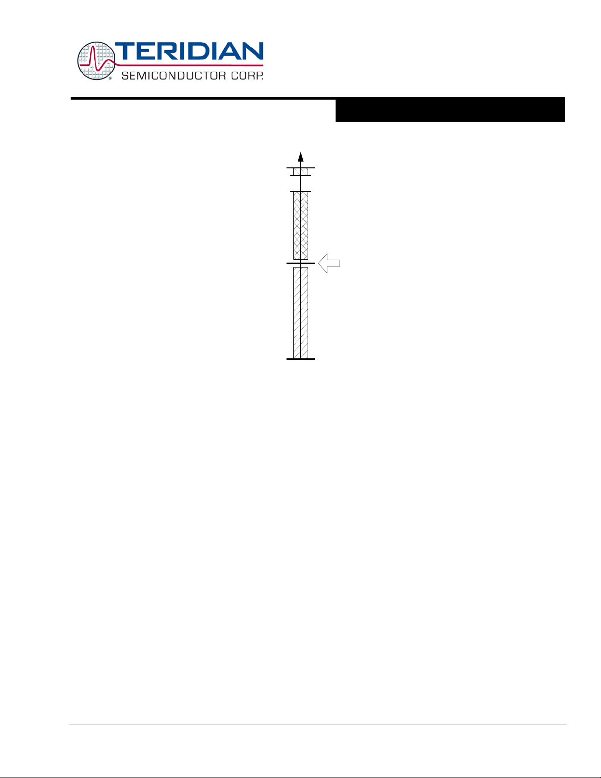
71M6513/71M6513H
3-Phase Energy Meter IC
DATA SHEET
A Maxim Integrated Products Brand
V3P3
V3P3 400mV
V3P3-10mV
VBIAS
0V
Battery or
reset
mode
Normal
operation,
WDT
enabled
WDT dis-
abled
V1
when
(V1 < VBIAS)
the battery is
enabled
SEPTEMBER 2011
Figure 11: Voltage Range for V1
Internal Clocks and Clo ck Dividers
All internal clocks are based on the watch crystal frequency (CK32 = 32,768Hz) applied to the XIN and XOUT pins. The PLL
multiplies this frequency by 150 to 4.9152MHz. This frequency is supplied to the ADC, the FIR filter (CKFIR), the clock test
output pin (CKTEST), the CE DRAM and the clock generator. The clock generator provides two clocks, one for the MPU
(CK M PU) and one for the CE (CKCE) .
The MPU clock frequency is determined by the I/O RAM register MPU_DIV (0x2004[2:0]) and can be CE*2
where MPU_DIV varies from 0 to 7 (MPU_DIV is 0 on power-up). This makes the MPU clock scalable from 4.9152MHz down
to 38.4kH z.
The c irc uit als o generates a 2x MPU clock for use by the emulator. This clock is not generated when the I/O RAM register
ECK_DIS (0x2005[5]) is asserted by the MPU.
I2C Interface (EEP ROM)
A dedicated 2-pin serial interface implements an I2C driver that can be used to communicate wit h ex t er na l E EP RO M d ev i c es.
The interface can be m ultiplexed onto the DIO pins DIO4 (SCK) and DIO5 (SDA) by setti ng the I/O RAM register DIO_EEX
(0x2008[4]). The MPU communicates with the interface through two SFR registers: EEDATA (0x9E) and EECTRL (0x9F). If the
MPU wishes to write a byte of data to EEPROM, it places the data in EEDATA and then writes the ‘Transmit’ code to EECTRL.
The wr ite t o EECTRL initiates the transmit sequence. By observing the BUSY bit in EECTRL the MPU can determine when the
transmit operation is finished (i.e. when the BUSY bit transitions from 1 to 0). INT5 is also asserted when BUSY fal ls. The MPU
can then check the RX_ACK bit to see if the EEPROM acknowledged the transmission.
A by te i s r ead b y wri ti ng t h e ‘Rec eiv e’ c ommand to EECTRL and waiting for BUSY to fal l. Up on c ompl et ion , t he r ecei ved dat a
will appear in EEDATA.
The serial transmit and receive clock is 78kHz during each transmission, and SCL is held in a high state until the next
tr ansmi ssion. The bits in EECTRL are shown in Table 56.
The EEPROM interface can also be operated by controlling the DIO4 and DIO5 pins directly. However, controlling DIO4 and
DIO5 directly is discouraged, because it may tie up the MPU to t he point where it may become too busy to process
interrupts.
© 2005-2011 Teridian Semiconductor Corporation Page: 45 of 104
-
MPU_DIV Hz
Page 46
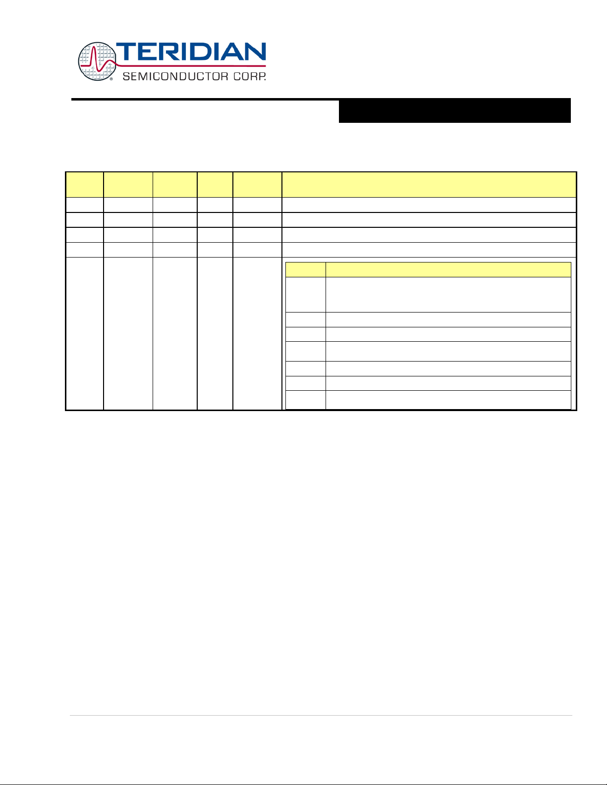
71M6513/71M6513H
3-Phase Energy Meter IC
DATA SHEET
A Maxim Integrated Products Brand
Bit
Write
State
4
TX_ACK
R
1
Negative
0 indicates when an ACK bit has been sent to the EEPROM
6
Rec eive the last byte fr om EEPROM and do not send ACK.
Note: Clock stretching and multi-master operation are not sup ported fo r the I2C int erface.
AUGUST 2011
Status
7 ERROR R 0 Positive 1 when an illegal command is received.
6 BUSY R 0 Positive 1 when serial data bus is busy.
5 RX_ACK R 1 Negative 0 indicates that the EEPROM sent an ACK bit.
3-0 CMD[3:0] W 0
Name
Read/
Reset
Polarity Description
CMD Operation
0 No-op. Applying the no-op command will stop the I2C clock
(SC K, DIO4). Fai lure to issue the no -op command will keep
the SCK signal toggling.
Positive,
see CMD
Table
Table 56: EECTRL Status Bits
2 Rec eive a b y te from EEPRO M and send ACK.
3 Transmit a byte to EEPROM.
5 Issue a ‘ST OP’ sequence.
9 Issue a ‘ST ART’ s equence.
Others No Operation, set the ERROR bit.
Page: 46 of 104 © 2005-2011 Teridian Semiconductor Corporation
Page 47
71M6513/71M6513H
3-Phase Energy Meter IC
DATA SHEET
A Maxim Integrated Products Brand
7
digital
V3_OK (Comparator 3 Output)
D
digital
RTCLK
SEPTEMBER 2011
Battery
The VBAT pin provides an input for an external battery that can be used to support the crystal oscillator, RTC, the WD_OVF bit
and XRAM in the absence of the main power supply. If the battery is not used, the VBAT pin should be connected to V3P3.
Internal Voltages (VBIAS, VBAT, V2P5)
The 71M6513 requires two supply voltages, V3P3A, for the analog section, and V3P3D, for the digital section. Both voltages
can be tied together outside the chip. The internal supply voltage V2P5 is generated by a regulator from the 3.3V supplies.
The battery voltage, VBAT, is required when crystal oscillator, RTC and XRAM are required to keep operating while V3P3D is
removed (battery m ode). VBAT, usually supplied by an external battery, powers crystal oscillator, RTC and XRAM (and the
WD_OVF bit).
VBIAS (1.5V) is generated internally and used for the comparators V1, V2 and V3.
Test Ports
TMU XO UT P i n: One out of 16 digital or 4 analog signals can be selected to be output on the TMUXOUT pin. The function of
the multiplexer is control led wit h the I/O RAM reg ister TMUX (0x2000[3:0]), as shown in Table 57.
TMUX[3:0] Mode Function
0 analog DGND
1 analog IBIAS
2 analog PLL_2.5V
3 analog VBIAS
4 digital RTM (Real ti me output fr om CE)
5 digital WDTR_EN (Comparator 1 Output AND V1LT3)
6 digital V2_OK (Comparator 2 Output)
8 digital RXD (from Optical interface)
9 digital MUX_SYNC
A digital CK_10M
B digital CK_MPU
C -- reserv ed for produ ctio n t est
E digital CE_BUSY
F digital XFER_BUSY
Table 57: TMUX[3:0] Selections
Emulator Port: The emulator port, consisting of the pins E_RST, E_TCLK and E_RXTX provides control of the MPU through
an external in-circuit emulator. The E_TBUS[3:0] pins, together with the E_ISYNC/BRKRQ add trace capability to the
emulator . The emulat or port i s compatible with the ADM51 emulators m anufa ctured by Sig num Systems.
The s ignals of th e emula tor por t have weak pull-ups. Adding 1kΩ pull-up resistors on the PCB is recommended.
Real-Time Monitor: The RTM output of the CE is available as one of the digital multiplexer options. RTM data is read from the
CE DRAM locations specified by I/O RAM registers RTM0, RTM1, RTM2, and RTM3 after the rise of MUX_SYNC. The RTM can
be enabled and disabled with I/O RAM register RTM_EN. The RTM output is clocked by CKTEST. Each RTM word is clocked
© 2005-2011 Teridian Semiconductor Corporation Page: 47 of 104
Page 48
71M6513/71M6513H
3-Phase Energy Meter IC
DATA SHEET
A Maxim Integrated Products Brand
SCLK
SEG3
AUGUST 2011
out in 35 cycles and contains a leading flag bit. Figure 13 in the Syst em Timi ng Sect ion illust rates the RTM output form at . RTM
is low when not in use.
SSI I nterface: A hig h-speed serial interface with handshake capability is available to send a contiguous block of CE data to an
external data logger or DSP. The block of data, configurable as to location and size, is sent starting 1 cycle of 32kHz before
each CE code pass begins. If the block of data is big enough that transmission has not completed when the code pass begins,
it will complete during the CE code pass with no timing impact to the CE or the serial data. In this case, care must be taken
that the transmitted data is not modified unexpectedly by the CE. The SSI interface is enabled by the SSI_EN bit and consists
of SCLK, SSDATA, and SFR as outputs and, optionally, SRDY as input. The interface is compatible with 16bit and 32bit
processors. The operation of each pin is as follows:
SCLK is the serial clock. The clock can be 5MHz or 10MHz, as specified by the SSI_10M bit. The SSI_CKGATE bit c ontr ols
whether SCLK runs continuously or is gated off when no SSI activity is occurring. If SCLK is gated, it will begin 3 cycles before
SFR r ises and will persist 3 cyc les after th e last d ata bit i s outpu t.
The p in s u sed f o r t he S SI ar e mul ti plex ed with the LCD segment outputs, as shown in Table 58. Thus, the LCD should be
disabled when the SSI is in use.
SSI Signal
SSDATA SEG4
SFR SEG5
SRDY SEG6
Table 58: SSI Pin Assignment
SRDY is an optional handshake input that indicates that the DSP or data-logging device is ready to receive data. SRDY must
be true (the polarity of SRDY is selectable with SSI_FPOL) to enable SFR to ri se and initiate the transfer of the next field. It is
expected that SRDY changes state on the rising edges of SCLK. If SRDY is not true when the SSI port is ready to transmit the
next field, transmission will be delayed until it is. SRDY is ignored except at the beginning of a field transmission. If SRDY is
not enabled (by SSI_RDYEN), the SSI port will behave as if SRDY is always true.
SSDATA is the serial output data. SSDATA changes on the rising edge of SCLK and outputs the contents of a block of CE
RAM words starting with address SSI_STRT and ending wit h SSI_END. The w ords are outp ut MSB first.
The f i el d si ze is set wi th th e SSI_FSIZE register: 0 entire data block, 1-8 b it fields, 2-16 bit fields, 3-32 bit fi el d s . T h e po l ar i ty of
the SFR pulse can be inverted with SSI_FPOL (SSI_FPOL = 0 SRDY high -active). If SRDY does not delay it, the first SFR
pulse in a frame will rise on the third SCLK after MUX_SYNC (or the fourth SCLK if 10MHz). MUX_SYNC can be used to
synchro nize the fields arriving at the data logger or DSP.
LCD Segment
Output Pin
Page: 48 of 104 © 2005-2011 Teridian Semiconductor Corporation
Page 49
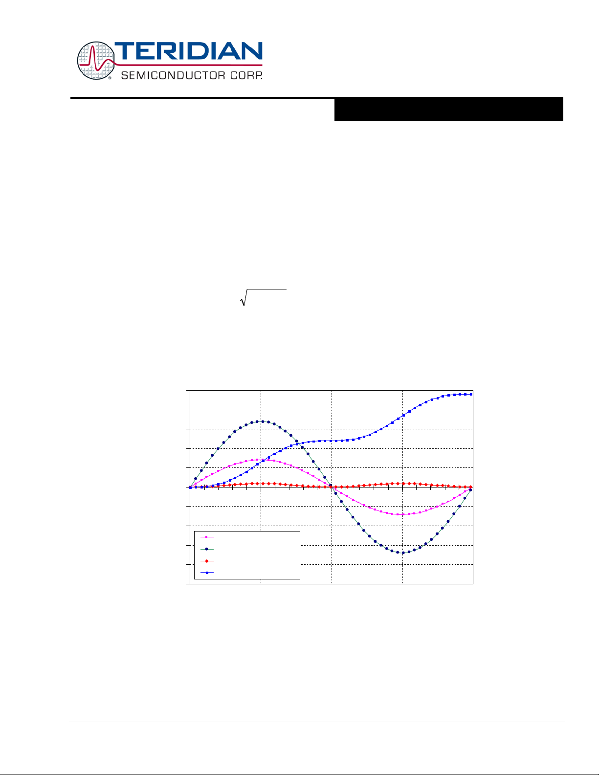
3-Phase Energy Meter IC
DATA SHEET
A Maxim Integrated Products Brand
∫
=
t
dttItVE
0
)()(
22
QP +
-500
-400
-300
-200
-100
0
100
200
300
400
500
0 5 10 15 20
time [ms]
V [V], I [A], P [Ws]
Current [A]
Voltage [V]
Energy per Interval [Ws]
Accumulated Energy [Ws]
FUNCTIONAL DESCRIPTION
Theory of Operation
The energy deli vered b y a power source into a load can be expressed as:
Assuming phase angles are constant, the follow ing formulae apply:
P = Real Energy [Wh] = V * A * cos φ* t
Q = Rea ctiv e Energ y [VARh] = V * A * sin φ * t
71M6513/71M6513H
SEPTEMBER 2011
S = Apparent Energy [VAh] =
For a practical meter, not only voltage and current amplitudes, but also phase angles and harmonic content may change
constantly. Thus, simple RMS measurements are inherently inaccurate. A m odern solid-sta te el ec tri ci ty met er I C suc h as t he
71M6513/6513H functions by emulating the integral operation above, i.e. it processes current and voltage samples through an
ADC at a constant frequency. As long as the ADC resolution is high enough and the sample frequency is beyond the harmonic
range of interest, the current and voltage samples, multiplied with the time period of sampling will yield an accurate quantity for
the momentary energy . Summ i ng up the momen tary en ergy qu antities o ver time will result in acc umula ted energy.
Figure 12 s ho ws t he s h ap es of V( t ) , I( t) , t h e m omentar y en er gy a n d t h e t ot al ac cum ulat ed en er gy , r es u lt i ng f r om 5 0 s am pl es
of the voltage and current signals over a period of 20ms. The application of 240VAC and 100A results in an accumulation of
480Ws over the 20ms period, as indicated by the curve for Accumulated Energy.
The d escribed s ampling method works reliably, even in the presenc e of dyn amic p hase shift and harmonic di stort ion.
© 2005-2011 Teridian Semiconductor Corporation Page: 49 of 104
Figure 12: Voltage. Current, Momentary and Accumulated Energy
Page 50
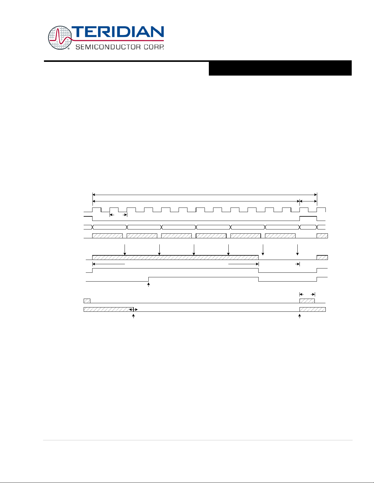
71M6513/71M6513H
3-Phase Energy Meter IC
DATA SHEET
A Maxim Integrated Products Brand
CK32
MUX STATE
00 1 2 3 4 5
MUX_DIV Conversions (MUX_DIV=6 i s shown)
Settle
ADC MUX Frame
ADC EXECUTION
S
MUX_SYNC
S
CE_EXECUTION
RTM
140
SSI
MAX CK COUNT
BEGIN SSI TRANSFERLAST SSI TRANSFER
0 300
150
600 900 1200 1500 1800
ADC0 ADC1 ADC2 ADC3 ADC4 ADC5
CK COUNT = CE_CYCLES + floor(CE_CYCLES + 2) / 5)
NOTES:
1. ALL DIMENSIONS ARE 5MHZ CK COUNTS.
2. THE PRECISE FREQUENCY OF CK IS 150*CRYSTAL FREQUENCY = 4.9152MHz.
3. XFER_BUSY OCCURS ONCE EVERY (PRESAMPS * SUM_CYCLES) CODE PASSES.
CE_BUSY
XFER_BUSY
INITIATED BY A CE OPCODE AT END OF SUM INTERVAL
ADC TIMING
CE TIMING
RTM and SSI TIM ING
AUGUST 2011
System Timing Summary
Figure 13 summarizes the timing relationships between the input MUX states, the CE_BUSY signal, and the two serial output
str eam s . I n th i s exa mple, MUX_DIV=0 (six mux states) and FIR_LEN = 0 ( 2 CK32 cycles). Since F IR fi lter conversions req uire
two or three CK32 cycles, the duration of each MUX cycle is 1 + 2 * states defined by MUX_DIV if FIR_LEN = 0, and 1 + 3 *
states defined by MUX_DIV if FIR_LEN = 1. Followed by the conversions is a single CK32 cycle.
Each CE program pass begins when MUX_SYNC falls. Depending on the length of the CE program, it may continue running
until the end of the ADC5 conversion. CE opcodes are constructed to ensure that all CE code passes consum e exactly the
sam e num ber of cycles. The result of each ADC conversion is inserted into the CE DRAM when the conversion is complete.
The CE code is designed to tolerate sudden changes in ADC data. The exact CK count when each ADC value is loaded into
DRAM is shown in Figure 13.
Figure 13 also shows that the two serial data streams, RTM and SSI, begin transmitting at the beginning of MUX_SYNC. RT M ,
consisting of 140 CK cycles, will always finish before the next code pass starts. The SSI port begins transmitting at the same
time as RTM, but may significantly overrun the next code pass if a large block of data is required. Neither the CE nor the SSI
port will be affected by this overlap.
Figure 14, Figure 15, and Figure 16 show the RTM and SSI timing, respectively.
Figure 13: Timing Relationship between ADC MUX, CE, and Serial Transfers
Page: 50 of 104 © 2005-2011 Teridian Semiconductor Corporation
Page 51
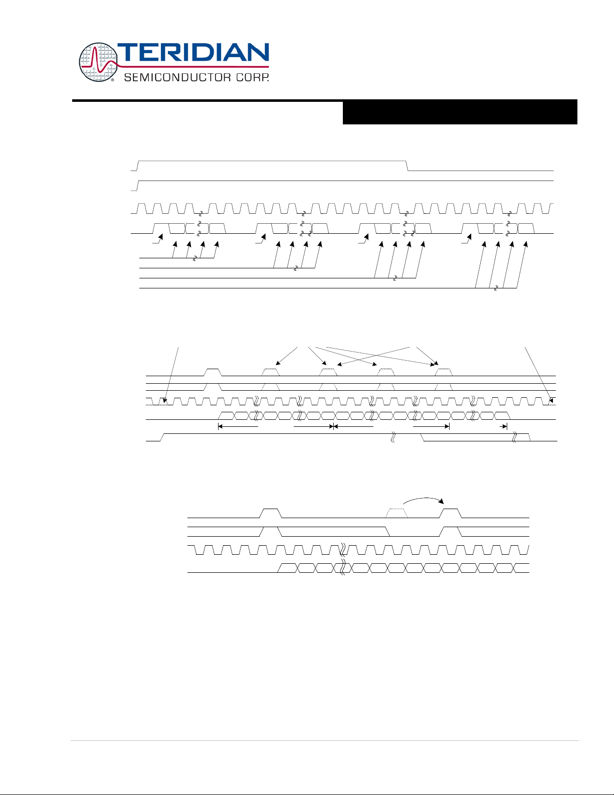
71M6513/71M6513H
3-Phase Energy Meter IC
DATA SHEET
A Maxim Integrated Products Brand
CKTEST
TMUXOUT/RTM
FLAG
RTM DATA0 (32 bits)
LSB
SIGN
LSB
SIGN
RTM DATA1 (32 bits)
LSB
LSB
SIGN
SIGN
RTM DATA2 (32 bits)
RTM DATA3 (32 bits)
0 1 30 31 0 1 30 31 0 1 30 31
0 1 30 31
FLAG
FLAG
FLAG
MUX_SYNC
CK32
SCLK (Output)
SSDATA (Output)
SFR (Output)
SRDY (Input)
31 30
16 15
1 0 31
SSI_BEG
30
16 15
1 0 31
SSI_BEG+1
1 0
SSI_END
If 16bit fields If 32bit fields
If SSI_CKGATE =1
If SSI_CKGATE =1
MUX_SYNC
SCLK (O utput)
SSDATA (Output)
SFR ( Output )
SRDY ( Input)
31 30 16 15 14 13
16 16 16
12
29 18
17
Next field is delayed wh i le SRDY is low
SEPTEMBER 2011
Figure 14: RTM Ou tp ut Format
Figure 15: SSI Timing, (SSI_FPOL = SSI_RDYPOL = 0)
Figure 16: SSI Timing, 16-bit Field Example (External Device Delays SRDY)
SFR is the framing pulse. Although CE words are always 32 bits, the SSI interface will frame the entire data block as a single
fi el d, a s m ul ti ple 16-b i t fi el d s , or a s m ul ti ple 32-bit f ields. The SFR pulse is one SCLK clock cycle wide, changes state on the
ri s ing edg e of SCLK and pr ecedes t he first bit of each f ield.
© 2005-2011 Teridian Semiconductor Corporation Page: 51 of 104
Page 52
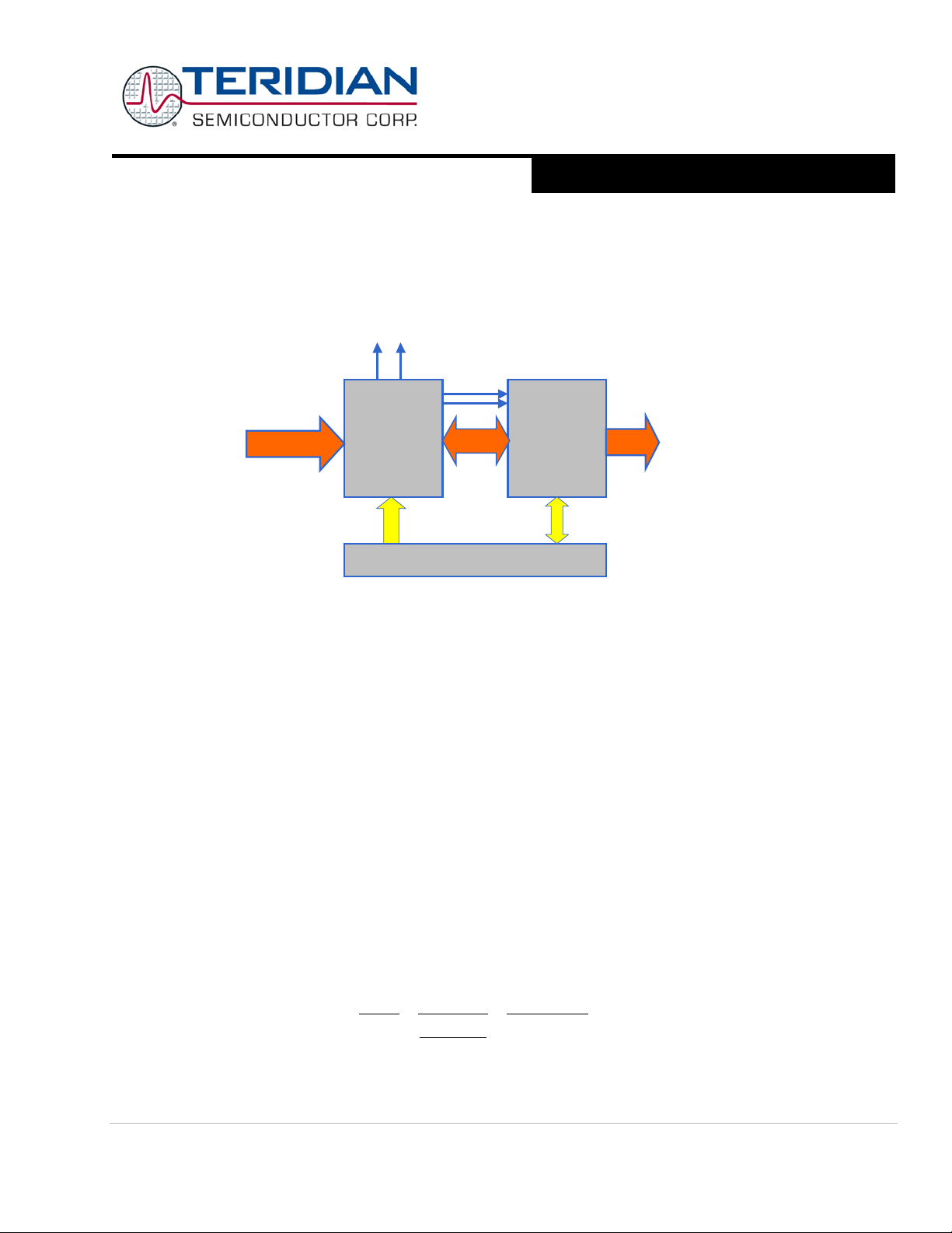
71M6513/71M6513H
3-Phase Energy Meter IC
DATA SHEET
A Maxim Integrated Products Brand
ms
Hz
Hz
f
N
S
ACC
75.999
62.2520
2520
13
32768
4260==⋅
==
τ
CE MPU
Pre-
Processor
Post-
Processor
IRQ
Processed
Metering
Data
Pulses
I/O RAM (Configuration RAM)
Samples Data
AUGUST 2011
Data Flow
The data flow between CE and MPU is shown in Figure 17. In a typical application, the 32-bit compute engine (CE)
sequentially processes the samples from the voltage inputs on pins IA, VA, IB, VB, IC, and VC performing calculations to
mea s ur e a ct i v e po w er (Wh), r ea c tive po wer (VARh ) , A
accessed by the MPU, processed further and output using the peripheral devices available to the MPU.
2
h, and V2h for four-quadrant metering. These measurements are then
Figure 17: MPU/CE Data Flow
CE/MPU Communication
Figure 18 shows the functional relationship between CE and MPU. The CE is controlled by the MPU via shared registers in the
I/O RAM and by registers in the CE DRAM. The CE outputs two interrupt signals to the MPU: CE_BUSY and XFER_BUSY,
which are connected to the MPU interrupt service inputs as external interrupts. CE_BUSY indicates that the CE is actively
processing data. This signal will occur once every multiplexer cycle. XFER_BUSY indicates that the CE is updating data to the
output region of the CE RAM. This will occur whenever the CE has finished generating a sum by completing an accumulation
interval determined by SUM_CYCLES * PRE_SAMPS samples. Interrupts to the MPU occur on the falling edges of the
XFER_BUSY and CE_BUSY signals.
Figure 19 shows the sequence of events between CE and MPU upon reset or power-up. In a typical application, the sequence
of events is as follows:
1) Upon power-up, t he MPU i nit i alizes the hardware, including disabling the CE
2) The MPU loads the code for the CE into the CE PRAM
3) The MPU loads CE data into the CE DRAM.
4) The MPU s tarts t he CE by setti ng the CE_EN bit in the I/ O RAM.
5) The CE then repetitively executes its code, gener ating results and storing them in the CE DRAM
It is important to note that the length of the accumulation interval, as determined by N
PRE_SAMPS i s no t an exac t m ulti pl e of 100 0ms . For exa m ple, if SUM_CYCLES = 60, and PRE_SAMPS = 00 ( 42) , th e res ul ti ng
accumulation interval is:
, the product of SUM_CYCLES and
ACC
This mean s t hat ac c urate t i me measurements require the RT C .
Page: 52 of 104 © 2005-2011 Teridian Semiconductor Corporation
Page 53
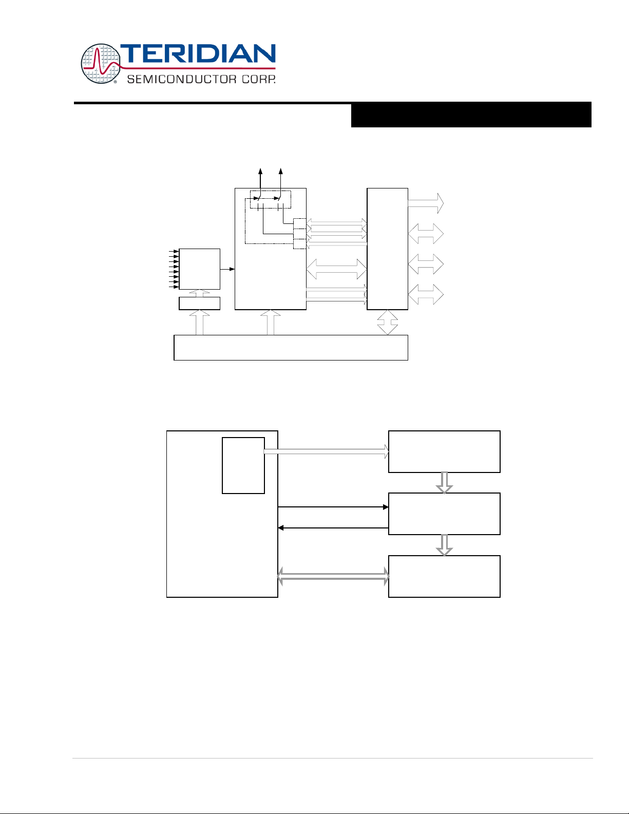
71M6513/71M6513H
3-Phase Energy Meter IC
DATA SHEET
A Maxim Integrated Products Brand
I/O RAM (CONFIGURATION RAM)
MPU
CE
PULSES
DATA
INTERRUPTS
DISPLAY (me-
mory-mapped
LCD segments)
DIO
EEPROM
(I2C)
SERIAL
(UART0/1)
SAMPLES
APULSEW
APULSER
VAR (DIO7) W (DIO6)
VARSUM
WSUM
ADC
EXT_PULSE
CE_BUSY
XFER_BUSY
Mux Ctrl.
CE_EN
CE PRAM
COMPUTATION
ENGINE
CE DRAM
FLASH
MPU
XFER Interrupt
SEPTEMBER 2011
Figure 18: MPU/CE Communication (Functional)
The MPU will wait for the CE to signal that fresh data is ready (the XFER interrupt). It will read the data and perform additional
processing such as energy accumulation.
Figure 19: MPU/CE Communication (Processing Sequence)
Reset Mode: When the RESETZ pin is pulled low or when V1 < VBIAS, all digital activity in the chip stops while analog circuits
are still active. The oscillator and RTC module continue to run. Additionally, all I/O RAM bits are cleared. As long as V1, the
input voltage at the power fault block, is greater than VBIAS, the internal 2.5V regulator will continue to provide power to the
digital secti on.
Onc e init iat ed, th e reset mode w ill persi st u ntil t he res et ti mer t imes o ut, si gnif ied by WAKE risi ng. Thi s wil l occ ur in 4100
cycles of the real time clock after RESETZ goes high, at which time the MPU will begin executing its preboot and boot
sequ ences from address 00. See the security section for m ore description of preboot an d boot.
© 2005-2011 Teridian Semiconductor Corporation Page: 53 of 104
Fault, Reset, Power-Up
Page 54
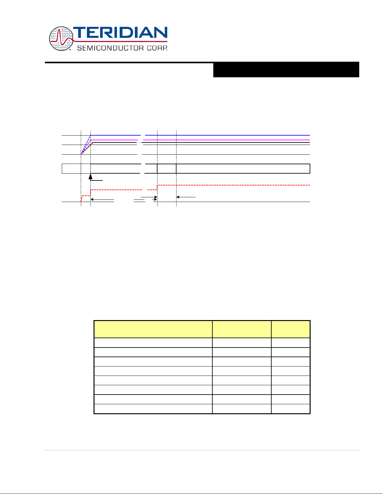
71M6513/71M6513H
3-Phase Energy Meter IC
DATA SHEET
A Maxim Integrated Products Brand
Typical
FLASH66Z
LCD_BSTEN
V3P3
V1
SUPPLY CURRENT
3.3V
1.5V
PRE-
BOOT
RESET TIMER
FIRMWARE HAS CONTROL OVER CHIP...
1ms
0V
V2P5
POWER
DOWN
V1 > VBIAS
PWR
UP
0mA
nominal
125ms
AUGUST 2011
Power-Up: Af t er p ow er -up, the 71M6513/6513H is in reset as long as V1 < VBIAS. As soon as V1 exceeds VBIAS, the reset
tim er i s st ar ted whi ch tak es th e MPU out of res et af t er 4 100 o sci ll ato r c ycl es ( see Figure 20) . Th e MPU th en i nit iat es it s pr eboot phase lasting 32 cycles. The supply current will be low but not zero duri ng power-up. It will increase, once V1 exceeds
VBIAS and will increase to the nominal value once the preboot phase starts. The supply current may then be reduced under
firmware control, following the steps specified in Battery Operation and Power Save Modes.
Figure 20: Timing Diagram for Voltages, Current and Operation Modes after Power-Up
When V1 is lower than VBIAS, the external battery will power the following parts of the 71M6513/6513H:
• RTC
• Crystal oscill a tor circuitry
• MPU XRAM
• WD_OVF bit
In normal mode of operation, running on 3.3V supply, various resources of the 71M6513/6513H may be shut down by the
MPU firmware in order to reduce power consum ption while other essential resources such as UARTs may remain active.
Table 59 outlines t hese res ources and t heir t ypical current con sumption ( based on initial co ndition MPU_DIV = 0) .
Power Saving Measure Software Control
Disable the CE CE_EN = 0 0.16mA
Disable the ADC ADC_DIS = 1 1.8mA
Disable clock test output C KTEST CKOUTDIS = 1 0.6mA
Disable emulator clock ECK_DIS = 1 *) 0.1mA
Set f lash read pulse timing to 33 ns
Disable the LCD v oltag e boost c i rcui t ry
Disable R TM outputs RTM_EN = 0 0.01mA
Increase the clock divider for th e M P U MPU_DIV = X 0.4mA/MHz
*) This bit is to be used with caution! Inadvertently setting this bit will inhibit access to the part with the ICE interface and thus
preclude flash erase and programming operations.
Page: 54 of 104 © 2005-2011 Teridian Semiconductor Corporation
Battery Operation
Power Save Modes
Table 59: Power Saving Measures
Savings
=1 0.04mA
= 0 0.9mA
Page 55
71M6513/71M6513H
3-Phase Energy Meter IC
DATA SHEET
A Maxim Integrated Products Brand
[1]
[0]
Function
SEPTEMBER 2011
Temperature Compensation
Internal Compensation: The internal voltage reference is calibrated during device manufacture. Trim data is stored in on-chip
fuses.
For the 71M6513, the temperature coefficients TC1 and TC2 are given as constants that represent typical component
behavior.
For the 71M6513H, the temperature characteristics of the chip are measured during production and then stored in the fuse
registers TRIMBGA, TRIMBGB and TRIMM[2:0]. TC1 and TC2 can be derived from the fuses by using the relations given in the
Electrical Sp ecificati ons sec t ion. TC1 and T C2 can be furth er processed to generate the co ef ficients PPMC and PPMC2.
TRIMM[2:0], TRIMBGA and TRIMBGB ar e read by first writing either 4, 5 or 6 to TRIMSEL (0x20FD) and then reading the value
of TRIM (0x20FF).
When the EXT_TEMP register in CE DRAM (address 0x38) is set to 0, the CE automatically compensates for temperature
errors by controlling the GAIN_ADJ register (address 0x2E) based on the PPMC, PPMC2, and TEMP_X r egi st er v alu es. In t he
case of internal compensation, GAIN_ADJ is an output of the CE.
External Compensation: Rather than internally compensating for the temperature variation, the bandgap temperature is
provided to the embedded MPU, which then may digitally compensate the power outputs. This permits a system-wide
temperature correction over the entir e system rather than local to the chip. The incorporated thermal coefficients may include
the current sensors, the voltage sensors, and other influences. Since the band gap is chopper stabilize d via the CHOP_EN bits,
the most significant long-term drift mechanism in the voltage reference is removed.
When the EXT_TEMP r egi st er i n CE DRA M is s et to 1 5, t he CE ig nor es t he PPMC, PPMC2, and TEMP_X r egister values and
applies the gain supplied by the MPU in GAIN_ADJ. Exter n al compen sat ion ena b l es th e MP U t o c on tr o l t he C E g ai n ba sed o n
any variable, and when EXT_TEMP = 15, GAIN_ADJ is an input to the CE.
Chopping Circuitry
As explained in the hardware section, the bits of the I/O RAM register CHOP_EN[1:0] have to be toggled in between
mul tiplexer cycles to achieve the desired eli minat ion of D C offset .
The amplifier wi th i n t h e r ef er en c e i s aut o -zeroed by means of an internal signal that is controlled by the CHOP_EN b its. When
thi s si gn al i s HIG H, th e con nec ti on of th e amp li fi er i np uts is r ever sed . T hi s pr eser ves th e ov era ll pol ar ity of the am pl ifi er gain
but inverts the input o ffset. By alter natel y reversing the c onnectio n, the offset of the amplifier is averaged to zero. The two bits
of the CHOP_EN register have the function specified in Table 60.
CHOP_EN
0 0 Toggle chop signal
0 1 Reference connection positive
1 0 R eference connection revers ed
1 1 Toggle chop signal
For automatic chopping, the CHOP_EN bits ar e set to either 00 or 11. In this mode, the polarity of the signals feeding the
ref erence a mpl ifier will b e autom atic ally t oggl ed for ea ch mul tipl exer cy cle as shown i n Figure 21. With an even n umber o f
mul tiplexer cycles in each accumulation interva l, the number of cycles with pos i tive reference connection wi ll equ al the number
of cycles with reversed connection, and the offset for each sampled signal will be averaged to zero. This sequence is
acceptable when only the primary signals (meter voltage, meter current) are of interest.
CHOP_EN
Table 60: CHOP_EN Bits
© 2005-2011 Teridian Semiconductor Corporation Page: 55 of 104
Page 56
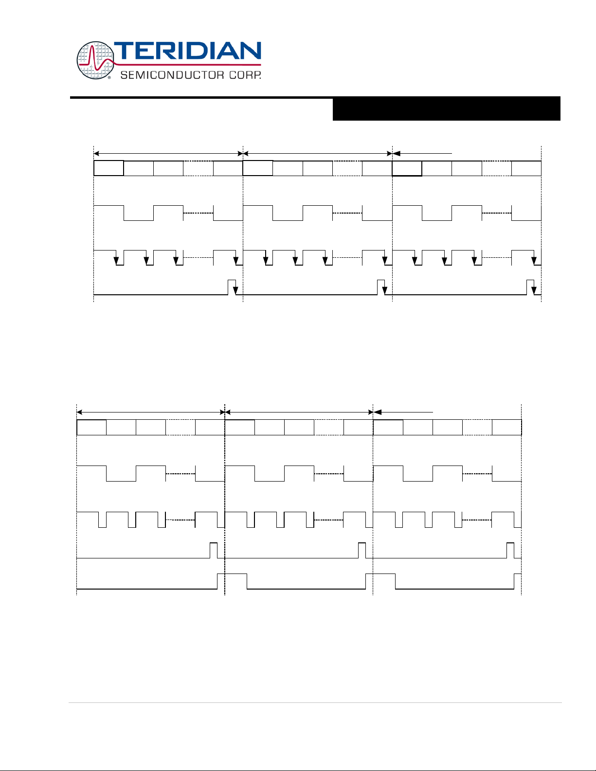
71M6513/71M6513H
3-Phase Energy Meter IC
DATA SHEET
A Maxim Integrated Products Brand
Accumulation Interval m
MUX
cycle n
MUX
cycle 2
MUX
cycle 3
Chop Polarity
Positive Positive
Positive Positive
Re-
versed
Re-
versed
Re-
versed
Re-
versed
MUX
cycle n
MUX
cycle 1
MUX
cycle 1
MUX
cycle 1
Accumulation Interval m+1
CE_BUSY interrupt
(falling edge)
XFER_BUSY interrupt
(falling edge)
Accumulation Interval m+2
Positive
Positive
Re-
versed
Accumulation Interval m
MUX
cycle n
MUX
cycle 2
MUX
cycle 3
Chop Polarity
Positive Positive
Positive Positive
Re-
versed
Re-
versed
Re-
versed
Re-
versed
MUX
cycle n
Accumulation Interval m+1
alt. MUX
cycle
alt. MUX
cycle
alt. MUX
cycle
CE_BUSY interrupt
XFER_BUSY interrupt
Accumulation Interval m+2
Positive Positive
Re-
versed
MUX_ALT
AUGUST 2011
Figure 21: Chop Polarity w/ Automatic Chopping
If temperature compensation or accurate reading of the die t emper atur e is requ ir ed, a lter nate m ul tipl exer cyc les h ave t o be
inserted in between the regular cycles. This is done under MPU firmware control by asserting the MUX_ALT bit whenever
necessary. Since die temperature usually changes very slowly, alternate multiplexer cycles have to be inserted very
infrequently. Usually, an alternate multiplexer cycle is inserted once for every accumulation period, i.e. after each
XFER _BUSY interrupt. This sequence is shown in Figure 22.
Figure 22: Sequence with Alternate Multiplexer Cycles
This sequence has the disadvantage that the alternate multiplexer cycle is always operated with positive connection.
Consequently, DC offset will appear on the temperature measurement, which will decrease the accuracy of this measurement
and thus cause temperature reading and compensation to be less accurate.
The sequence shown in Figure 23 uses t he CHOP_EN bits to control the chopper polarity after each XFER_BUSY interrupt.
CHOP_EN is controlled to alternate between 10 (positive) and 01 (reversed) for the first multiplexer cycle following each
Page: 56 of 104 © 2005-2011 Teridian Semiconductor Corporation
Page 57
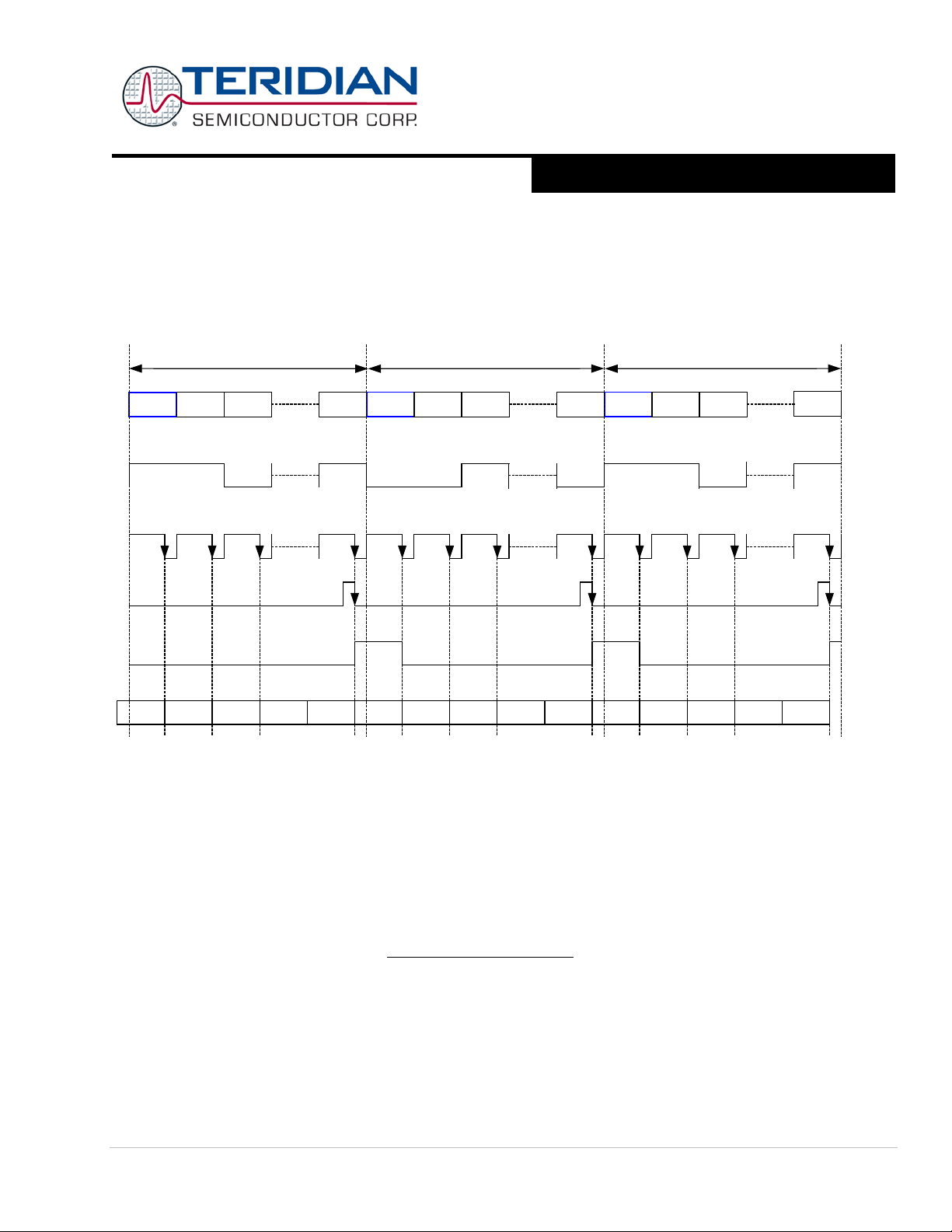
71M6513/71M6513H
3-Phase Energy Meter IC
DATA SHEET
A Maxim Integrated Products Brand
]/[
8_
1782.66
pulseWh
XNWRATEIn
IMAXVMAX
Kh
ACC
⋅⋅⋅
⋅⋅
=
alt. MUX
cycle
alt. MUX
cycle
alt. MUX
cycle
Accumulation Interval m Accumulation Interval m+1
Positive Positive
Positive Positive
Positive
Accumulation Interval m+2
Positive Positive
re-
versed
re-
versed
re-
versed
re-
versed
re-
versed
MUX
cycle 2
MUX
cycle 2
MUX
cycle 2
MUX
cycle 3
MUX
cycle 3
MUX
cycle 3
MUX
cycle n
MUX
cycle n
MUX
cycle n
Chop Polarity
01 11 01 11(11) (11) (11) (11)(11) (11)(11) 10 11 (11)
CHOP_EN
(11)
CE_BUSY interrupt
XFER_BUSY interrupt
MUX_ALT
SEPTEMBER 2011
XFER_BUSY interrupt. After these first two cycles, CHOP_EN returns to 11 ( automatic toggle). The value of CHOP_EN, when
set after the XFER_BUSY interrupt, is in force for the entire following multiplexer cycle.
When using this sequence, the alternate multiplexer cycle is toggled between positive and reversed connection resulting in
accurate temperature measurement.
An example for proper application of the CHOP_EN bits can be found in the Demo Code shipped wit h the 6513 Demo Kits.
Fir mware i mplem ent ati ons should closely follow this example.
Figure 23: Sequence with Alternate Multiplexer Cycles and Controlled Chopping
Internal/External Pulse Generation and Pulse Counting
The CE is the source for pulses. It can generate pulses directly based on the voltage and current inputs and the configured
pulse generation parameters. This is called “internal pulse generation”, and applies when the CE RAM register EXT_PULSE
(address 0x37) equals 0. Alternatively, the CE can be configured to generate pulses based on registers that are controlled by
the MPU (“external pulse generati on”), i.e. when the register EXT_PULSE equals 15. In the case of external pulse generation,
the M PU wri tes val ues to the CE regist ers APULSEW (0x26) and APULSER (0x27).
The pulse rate, usually inversely expressed as “Kh” (and measured in Wh per pulse), is determined by the CE RAM registers
WRATE, PULSE_SLOW, PULSE_FAST, In_8, as well as by the sensor scaling VMAX and IMAX per the equation:
where
In_8 is the gain factor (1 or 8) controlled by the CE variable In_SHUNT,
X is the pulse gain factor controlled by the CE variables PULSE_SLOW and PULSE_FAST
is the accumulation count (PRE_SAMPS * SUM_CYCLES)
N
ACC
© 2005-2011 Teridian Semiconductor Corporation Page: 57 of 104
Page 58

71M6513/71M6513H
3-Phase Energy Meter IC
DATA SHEET
A Maxim Integrated Products Brand
AUGUST 2011
Program Security
When enabled, the security feature limits the ICE to global flash erase operations only. All other ICE operations are blocked.
This guarantees the security of the user’s MPU and CE program code. Security is enabled by MPU cod e t ha t i s exec u t ed i n a
32 cycle preboot interval before the primary boot sequence begins. Once security is enabled, the only way to disable it is to
perform a global erase of the flash memory, followed by a chip reset. Global flash erase also clears the CE PRAM.
The first 32 cycles of the MPU boot code are called the preboot phase because during t his phase the ICE is inhi bited. A readonly status bit, PREBOOT (SFR 0xB2[7]), identifies these cycles to the MPU. Upon completion of the preboot sequence, the
ICE can be enabled and is permitted to take control of the MPU.
SECURE (SFR 0xB2[6]), the security enable bit, is reset whenever the MPU is reset. Hardware associated with the bit permits
only ones to be written to it. Thus, preboot code may set SECURE to ena bl e the s ecur ity feat ure b ut m ay not res et it . On ce
SECURE is set, the preboot code is protected and no external read of program code is possible.
Spec ificall y, when SECURE is set:
• The ICE is li mited to bulk flas h eras e only.
• Page zero of flash memory, the preferred location for the user’s preboot code, may not be page-erased by either MPU or
ICE. Page zero may only be erased with global flash erase. Note that global flash erase erase s CE program RAM whe the r
SECURE is set or not .
• Writes to page zer o, whether by MPU or ICE, are inhibited.
SECURE bit i s to be used with cauti on! I nadvertently setti ng this bit will inhibit access to the part via the ICE
The
interface, if no mechanism for actively resetting the part between reset and erase operations is provid ed (see I CE
Interface description).
Additionally, by setting the I/O RAM register ECK_DIS to 1, the emulator clock is disabled, inhibiting access to the program with
the emulator. See the cautionary note in the I/O RAM Register description!
Page: 58 of 104 © 2005-2011 Teridian Semiconductor Corporation
Page 59
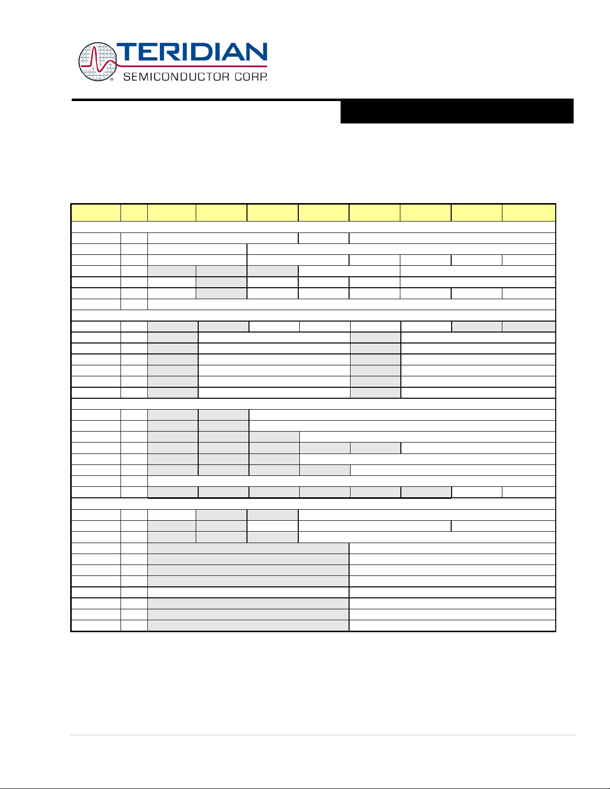
71M6513/71M6513H
3-Phase Energy Meter IC
DATA SHEET
A Maxim Integrated Products Brand
Configuration:
CE0
2000
EQU[2:0]
CE_EN
TMUX[3:0]
CE1
2001
PRE_SAMPS[1:0]
SUM_CYCLES[5:0]
CE2
2002
MUX_DIV[1:0]
CHOP_EN[1:0]
RTM_EN
WD_OVF
EX_RTC
EX_XFR
COMP0
2003
COMP_INT[1:0]
COMP_STAT[2:0]
CONFIG0
2004
VREF_CAL
RESERVED
CKOUT_DIS
VREF_DIS
MPU_DIV
CONFIG1
2005
RESERVED
ECK_DIS
FIR_LEN
ADC_DIS
MUX_ALT
FLASH66Z
MUX_E
VERSION
2006
VERSION[7:0]
Digital I/O:
DIO0
2008
OPT_TXDIS
DIO_EEX
DIO_PW
DIO_PV
DIO1
2009
DIO_R1[2:0]
DIO_R0[2:0]
DIO2
200A
DIO_R3[2:0]
DIO_R2[2:0]
DIO3
200B
DIO_R5[2:0]
DIO_R4[2:0]
DIO4
200C
DIO_R7[2:0]
DIO_R6[2:0]
DIO5
200D
DIO_R9[2:0]
DIO_R8[2:0]
DIO6
200E
DIO_R11[2:0]
DIO_R10[2:0]
Real Time Clock:
RTC0
2015
RTC_SEC[5:0]
RTC1
2016
RTC_MIN[5:0]
RTC2
2017
RTC_HR[4:0]
RTC3
2018
RTC_DAY[2:0]
RTC4
2019
RTC_DATE[4:0]
RTC5
201A
RTC_MO[3:0]
RTC6
201B
RTC_YR[7:0]
RTC7
201C
RTC_DEC_SEC
RTC_INC_SEC
LCD Display Interfac e:
LCDX
2020
LCD_BSTEN
LCD_NUM[4:0]
LCDY
2021
LCD_EN
LCD_MODE[2:0]
LCD_CLK[1:0]
LCDZ
2022
LCD_FS[4:0]
LCD0
2030
LCD_SEG0[3:0]
LCD1
2031
LCD_SEG1[3:0]
LCD2
2032
LCD_SEG2[3:0]
LCD3
2033
LCD_SEG3[3:0]
…
…
…
…
LCD39
2057
LCD_SEG39[3:0]
LCD40
2058
LCD_SEG40[3:0]
LCD41
2059
LCD_SEG41[3:0]
SEPTEMBER 2011
FIRMWARE INTERFACE
I/O RAM MAP – In Numerical Order
‘Not Used’ bits are blacked out and contain no memory and are read by the MPU as zero. RESERVED bi ts are in use and
should not be changed.
Name Addr Bit 7 Bi t 6 Bit 5 Bit 4 Bit 3 Bit 2 Bit 1 Bit 0
© 2005-2011 Teridian Semiconductor Corporation Page: 59 of 104
Page 60
71M6513/71M6513H
3-Phase Energy Meter IC
DATA SHEET
A Maxim Integrated Products Brand
RTM Probes:
RTM0
2060
RTM0[7:0]
RTM1
2061
RTM1[7:0]
RTM2
2062
RTM2[7:0]
RTM3
2063
RTM3[7:0]
Synchronous Serial Interface:
SSI
2070
SSI_EN
SSI_10M
SSI_CKGATE
SSI_FSIZE[1:0]
SSI_FPOL
SSI_RDYEN
SSI_RDYPOL
SSI_BEG
2071
SSI_END
2072
SSI_END[7:0]
Fuse Selection Registers:
TRIMSEL
20FD
TRIMSEL[7:0]
TRIM
20FF
TRIM[7:0]
SFR
Addr
Digital I/O:
P0
80
DIO_0[7:0] (Port 0)
DIR0
A2
DIO_DIR0[7:0]
P1
90
DIO_1[7:0] (Port 1)
DIR1
91
DIO_DIR1[7:0]
P2
A0
DIO_2[5:0] (Port 2)
DIR2
A1
DIO_DIR2[5:0]
Interrupts and WD Timer:
INTBITS
F8
INT6
INT5
INT4
INT3
INT2
INT1
INT0
WDI
E8
WD_RST
IE_RTC
IE_XFER
Flash:
ERASE
94
FLSH_ERASE[7:0]
FLSHCTL
B2
PREBOOT
SECURE
FLSH_MEEN
FLSH_PWE
PGADR
B7
FLSH_PGADR[6:0]
Serial EEPROM:
EEDATA
9E
EEDATA[7:0]
EECTRL
9F
EECTRL[7:0]
AUGUST 2011
Name Addr Bit 7 Bi t 6 Bit 5 Bit 4 Bit 3 Bit 2 Bit 1 Bit 0
SSI_BEG[7:0]
SFR MAP (SFRs Specific to Teridian 80515) – In Numerical Order
‘Not Used’ bits are blacked out and contain no memory and are read by the MPU as zero. RESERVED bi ts are in use and
should not be changed. This table lists only the SFR registers that are not generic 8051 SFR registers.
Name
Bit 7 Bi t 6 Bit 5 Bit 4 Bit 3 Bit 2 Bit 1 Bit 0
Page: 60 of 104 © 2005-2011 Teridian Semiconductor Corporation
Page 61
71M6513/71M6513H
3-Phase Energy Meter IC
DATA SHEET
A Maxim Integrated Products Brand
RESERVED
2004[5]
R/W
Must be 0.
CKOUT_DIS
0
NONE
--
1
Reserved
OR
2
T0 (counter0 clock)
OR
3
T1 (counter1 clock)
OR
4
High priority I/O interrupt (int0 rising)
OR
5
Low priority I/O interrupt (int1 rising)
OR
6
High priority I/O interrupt (int0 falling)
OR
7
Low priority I/O interrupt (int1 falling)
OR
DIO_DIR0[7:0]
Programs the direction of DIO pins 7 through 0. 1 indicates output. Ignored if
SEPTEMBER 2011
I/O RAM (Configuration RAM) – Alphabetical Order
Many functions of the chip can be controlled via the I/O RAM (Configuration RAM). The CE will also take some of its parameters from the I/O RAM.
Bits with a W (write) direction are written by the MPU into I/O RAM. Typically, they are initially stored in flash memory and
copied to the I/O RAM by the MPU. Some of the more frequently programmed bits are mapped to the MPU SFR memory
spa ce. Th e rem ai ni ng bits are mapped to 2xxx. Bits with R (read) direction can only be read by the MPU. On power up, all
bits are cleared to zero unless otherwise stated. Generic SFR registers are not listed.
Name
ADC_DIS 2005[3] R/W Di sables ADC and removes bias current
CE_EN 2000[4] R/W CE enable.
CHOP_EN[1:0] 2002[5:4] R/W Chop enable for the reference band gap circuit.
COMP_INT[1:0] 2003[4:3] R/W Two bi ts establis hing wh ether a compa rator state change should crea te
COMP_STAT[2:0] 2003[2:0] R Three bits containing comparator output status.
DIO_R0[2:0]
DIO_R1[2:0]
DIO_R2[2:0]
DIO_R3[2:0]
DIO_R4[2:0]
DIO_R5[2:0]
DIO_R6[2:0]
DIO_R7[2:0]
DIO_R8[2:0]
DIO_R9[2:0]
DIO_R10[2:0]
DIO_R11[2:0]
Location
[Bit(s)]
2004[4] R/W CKOUT Disable. When zero, CKTEST is an active output.
2009[2:0]
2009[6:4]
200A[2:0]
200A[6:4]
200B[2:0]
200B[6:4]
200C[2:0]
200C[6:4]
200D[2:0]
200D[6:4]
200E[2:0]
200E[6:4]
Dir Description
00: enabled 01: disabled 10: disabled 11: enabled
MPU interrupts. 1: interr upt, 0: no interrupt. If 11, the comparator outputs a re
XOR’ed.
Bit0 = comp 2, Bit 1 = comp3
B it0 = comp1, Bi t1 = comp2, Bit2 = comp3
R/W
R/W
R/W
R/W
R/W
R/W
R/W
R/W
R/W
R/W
R/W
R/W
Connects dedicated I/O pins 0 to 11 to selectable internal resources. If more
than one input is connected to the same resource, the ‘Multiple’ column
below specifies how t hey are c ombined. See Soft w are User’s Guide fo r
details).
DIO_GP Resource Multiple
SFR A2 R/W
the pin is not configured as I/O. See DIO_PV and DIO_PW for special option
for DIO6 and DIO7 o utputs . See DIO_EEX f or special option for DIO4 and
DIO5.
DIO_DIR1[7:0] SFR 91 R/W Programs the direction of DIO pins 15 through 8. 1 indicates output. Ignored
if the pin is not configured as I/O.
DIO_DIR2[5:0] SFR
A1[5:0]
© 2005-2011 Teridian Semiconductor Corporation Page: 61 of 104
R/W Programs the direction of DIO pins 21 through 16. 1 indicates output.
Ignored if the pin is not configured as I/O.
Page 62
71M6513/71M6513H
3-Phase Energy Meter IC
DATA SHEET
A Maxim Integrated Products Brand
DIO_PV
EEDATA[7:0]
SFR 9E
R/W
Serial EEPROM interface data
EECTRL[7:0]
FLASH66Z
2005[1]
R/W
Sho uld be s et to 1 to minimize supply current.
FLSH_ERASE
FLSH_MEEN
SFR B2[1]
W
Mass Erase Enable
AUGUST 2011
Name
DIO_0[7:0]
DIO_1[7:0]
DIO_2[5:0]
DIO_EEX 2008[4] R/W When s et, converts D I O4 and D I O5 to interface with exter nal EEPROM.
DIO_PW 2008[3] R/W Causes WPULSE to be output on DIO6, if DIO6 is configured as output.
ECK_DIS 2005[5] R/W Emulator clock disable. When on e, the emulat or clo ck is disabled . This bit
EQU[2:0] 2000[7:5] R/W Specifies the power equation to the CE.
EX_XFR
EX_RTC
FIR_LEN 2005[4] R/W The length of the ADC decimation FIR filter.
Location
[Bit(s)]
SFR 80
SFR 90
SFR
A0[5:0]
2008[2] R/W Causes VARPULSE to be output on DIO7, if DIO7 is configured as output.
SFR 9F R/W Serial EE PROM in terfa ce control
2002[0]
2002[1]
Dir Description
R/W
R/W
R/W
R/W Interrupt enable bits. These bits enable the XFER_BUSY and the
Port 0
Port 1
Port 2
DIO4 becomes SCK and DIO5 becomes bi-direct ional SDA. LCD_NUM
must be less than 18.
LCD_NUM must be l ess than 15.
LCD_NUM must be l ess than 16.
is to be used with caution! Inadvertently setting this bit will
inhibit access to the part with the ICE interface and thus
preclude flash erase and programming operations. If ECK_DIS
is set, it should be done at least 1000ms after power-up to give emulators
and programming devices enough time to complete an erase operation.
RTC_1SEC interrupts to the MPU. Note that if either interrupt is to be
enabled, EX6 in the 80515 must also be set.
1: 22 ADC bits/3 CK32 cycles (384 CKFIR cycles),
0: 21 ADC bits/2 CK32 cycles (288 CKFIR cycles)
The value on the DIO pins. Pins configured
as LCD will read zero. When written,
changes data on pins configured as outputs. Pins configured as LCD or input will
ignore writes.
SFR 94 W Flash Er ase Ini tiat e
Page: 62 of 104 © 2005-2011 Teridian Semiconductor Corporation
FLSH_ERASE is us ed to initiate either the Flash M ass Era se cycle or th e
Flash Page Erase cycle. Specific patterns are expected for FLSH_ERASE in
order to i nitiate the appro priate Erase cycle.
(default = 0x00).
0x55 – Initiat e Flash P age Erase cycle. Mus t be proc eeded by a write to
FLSH_PGADR @ SFR 0xB7.
0xAA – Initiate Flas h M ass Er ase cycle. Mus t be proceeded by a write to
FLSH_MEEN @ SFR 0xB2 and the debug (CC) port must be
enabled.
Any other patter n writ ten to FLSH_ERASE will have no ef fect.
0 – Mass Eras e disabled (default).
1 – Mass Erase enabled.
Must be re-written for each new Mass Erase cycle.
Page 63

71M6513/71M6513H
3-Phase Energy Meter IC
DATA SHEET
A Maxim Integrated Products Brand
Flash Page Address (page 0 thru 127) that will be
rupt. The flags are set by
inputs. The MPU may read these bits to see the input to external
interrupts INT0, INT1, up to INT6. These bits do not have any memory and
LCD_BSTEN
2020[7]
R/W
Enables the LCD voltage boost circuit.
LCD_CLK[1:0]
Sets the LCD clock frequency for COM/SEG pins (not the frame rate. Note:
LCD_EN
Enables the LCD display. When disabled, VLC2, VLC1, and VLC0 are
)
31
_
3.07.0(
2
FSLCD
VLCDVLC +⋅=
SEPTEMBER 2011
Name
FLSH_PGADR SFR
FLSH_PWE SFR B2[0] R/W Program Write Enable
IE_XFER
IE_RTC
INTBITS SFR
LCD_FS[4:0] 2022[4:0] R/W Controls the LCD full scale voltage, VLC2:
Location
[Bit(s)]
B7[7:1]
SFR E8[0]
SFR E8[1]
F8[6:0]
2021[1:0] R/W
2021[5] R/W
Dir Description
W Flash Page Erase Address
R/W Interrupt flags. These flags are part of the WDI SFR register and monitor the
R Interrupt
FLSH_PGADR[6:0] –
erased during the Page Erase cycle. (default = 0x00).
Must be re-written for each new Page Erase cycle.
0 – MOVX commands refer to XRAM Space, normal operation (default).
1 – MOVX @DPTR,A moves A to Program Space (Flash) @ DPTR.
This bit is automatically reset after each byte written to flash. Writes to this
bit are inhibited wh en inter rupts are ena bled.
XFER_BUSY interrupt and the RTC_1SEC inter
hardware and must be cleared by the interrupt handl er. See also WD_RST.
are primarily intended for debug use.
fw = CKFIR/128
00: fw/29, 01: fw/28, 10: fw/27, 11: fw/26
ground as are the COM and SEG outputs.
LCD_MODE[2:0] 2021[4:2] R/W The LCD bias mode.
000: 4 states, 1/3 bias
001: 3 states, 1/3 bias
010: 2 states, ½ bias
011: 3 states, ½ bias
100: static display
© 2005-2011 Teridian Semiconductor Corporation Page: 63 of 104
Page 64
71M6513/71M6513H
3-Phase Energy Meter IC
DATA SHEET
A Maxim Integrated Products Brand
purpose LCD/DIO pins to be configured as LCD. This
= 2, SEG41 and SEG 40 will be
as LCD. The remaining SEG39 to SEG24 will be configured as
LCD_NUM
SEG
DIO
0
None
DIO4-21
1
SEG41
DIO4-20
2
SEG40-41
DIO4-19
3
SEG39-41
DIO4-18
4
SEG38-41
DIO4-17
5
SEG37-41
DIO4-16
6
SEG36-41
DIO4-15
7
SEG35-41
DIO4-14
8
SEG34-41
DIO4-13
9
SEG33-41
DIO4-12
10
SEG32-41
DIO4-11
11
SEG31-41
DIO4-10
12
SEG30-41
DIO4-9
13
SEG29-41
DIO4-8
14
SEG28-41
DIO4-7
15
SEG27-41
DIO4-6
16
SEG26-41
DIO4-5
17
SEG25-41
DIO4
18
SEG24-41
None
MUX_E
2005[0]
R/W
MUX_SYNC enable. When high, converts SEG7 into a MUX_SYNC output.
OPT_TXDIS
PREBOOT
AUGUST 2011
Name
LCD_NUM[4:0] 2020[4:0] R/W Number of dual-
Location
[Bit(s)]
Dir Description
number can be between 0 and 18. The first dual-purpose pin to be used as
LCD is SEG41/DIO21. If LCD_NUM
configured
DIO19 to DIO4.
LCD_SEG0[3:0]
…
LCD_SEG41[3:0]
MPU_DIV[2:0] 2004[2:0] R/W The MPU clock divi der (from CKCE ) . Thes e bits may be pr ogrammed by
MUX_ALT 2005[2] R/W The MPU asserts this bit when it wishes the MUX to perform ADC
MUX_DIV[1:0] 2002[7:6] R/W The number of states in the input multiplexer.
Page: 64 of 104 © 2005-2011 Teridian Semiconductor Corporation
2030[3:0]
…
2059[3:0]
2008[5] R/W Tristates the OPT_TX output.
SFR B2[7] R Indicates that the preboo t sequen ce is activ e.
R/W LCD Segment Data. E ach wor d conta ins information for from 1 to 4 time
div isio ns of each segm ent. I n each word, bit 0 corresponds to COM0, on up
to bit 3 for COM3.
the MPU without risk of losing control.
000 - CKCE, 001 - CKCE/2, …, 111 - CKCE/2
MPU_DIV is 000 on power-up.
conversions on an alternate set of inputs.
00 - 6 sta tes 01 - 4 states 10 - 3 states 11 - 2 states
7
Page 65
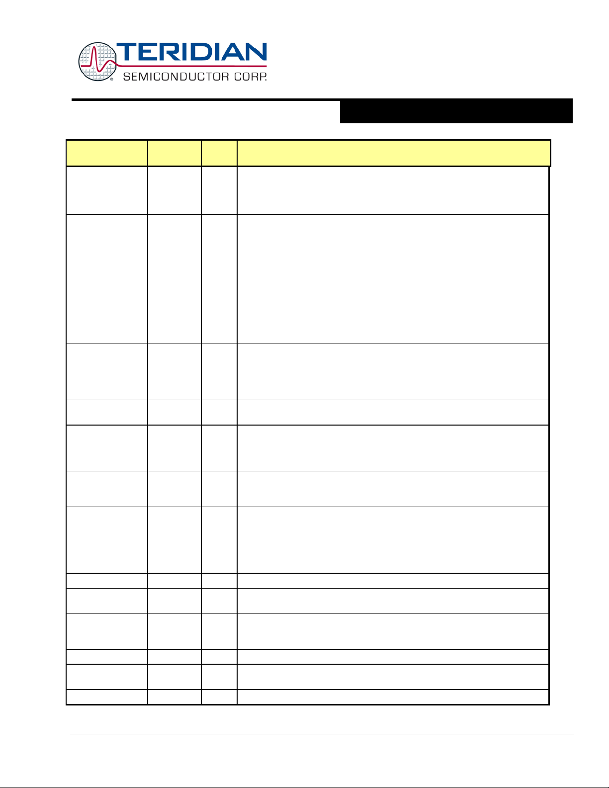
71M6513/71M6513H
3-Phase Energy Meter IC
DATA SHEET
A Maxim Integrated Products Brand
RTC_SEC[5:0]
2015
R/W
The RTC interface. These are the ‘year’, ‘month’, ‘day’, ‘hour’, ‘minute’ and
‘second’ parameters for the RTC. The RTC is set by writing to these
RTC_DEC_SEC
201C[1]
W
RTC time correction bits. Only one bit may be pulsed at a time. When
register is clocked. The
pulse width may be any value. If an additional correction is desired, the
Real Time Monitor enable. When ‘0’, the RTM output is low. This bit
RTM0[7:0]
SECURE
Enables security provisions that prevent external reading of flash memory
program RAM. This bit is reset on chip reset and may only be set.
SSI_EN
2070[7]
R/W
Enables the Synchronous Serial Interface (SSI) on SEG3, SEG4, and
is set, SEG6 is enabled also. The pins take on the
new functions SCLK, SSDATA, SFR, and SRDY, respectively. When
is low, these pins are converted to the SSI
SSI_CKGATE
2070[5]
R/W
SSI gated clock enable. When low, the SCLK is continuous. When high, the
SEPTEMBER 2011
Name
PRE_SAMPS[1:0] 2001[7:6] R/W Together w/ SUM_CYCLES, this v alue determines the number of samples in
RTC_MINI[5:0]
RTC_HR[4:0]
RTC_DAY[2:0]
RTC_DATE[4:0]
RTC_MO[3:0]
RTC_YR[7:0]
RTC_INC_SEC
RTM_EN 2002[3] R/W
RTM1[7:0]
RTM2[7:0]
RTM3[7:0]
Location
[Bit(s)]
2016
2017
2018
2019
201A
201B
201C[0]
2060
2061
2062
2063
SFR B2[6] R/W
Dir Description
R/W Four RTM probes. Before each CE code pass, the values of these registers
one s um cycle between XFE R interrupts for t he CE.
Num ber of samples = PRE_SAMPS*SUM_CYCLES.
00-42, 01-50, 10-84, 11-100
registers. Year 00 is defined as a leap year.
SEC 00 to 59
MIN 00 to 59
HR 00 to 23 (00=Midnight)
DAY 01 to 07 (01=Sunday)
DATE 01 to 31
MO 01 to 12
YR 00 to 256
pulsed, causes the RTC time value to be incremented (or decremented) by
an additional second the next time the RTC_SEC
MPU must wait 2 seconds before pulsing one of the bits again.
enables the two wire version of RTM
are serial ly output on the RTM pi n. The RTM registers are ignor ed when
RTM_EN=0.
and CE
Attempt s to write zero a re ignored.
SEG5 p ins. If SSI_RDYEN
SSI_EN is high and LCD_EN
function, regardless of LCDEN and LCD_NUM. For proper LCD operation,
SSI_EN must not be high when LCD_EN is high.
SSI_10M 2070[6] R/W SSI clock speed: 0: 5MHz, 1: 10MHz
clock is held low when data is not being transferred.
SSI_FSIZE[1:0] 2070[4:3] R/W SSI f rame pulse for mat:
0: once at beginning of SSI sequence (whole block of data),
1: every 8 bits, 2 : every 16 bits, 3: every 32 bi ts.
SSI_FPOL 2070[2] R/W SFR pulse polarity: 0: positive, 1: negat ive
SSI_RDYEN 2070[1] R/W SRDY enable. If SSI_RDYEN and SSI_EN are high, the SEG6 pin is
configured as SRDY. Otherwise, it is an LCD driver.
SSI_RDYPOL 2070[0] R/W SRDY polarity: 0: positive, 1: negative
© 2005-2011 Teridian Semiconductor Corporation Page: 65 of 104
Page 66

71M6513/71M6513H
3-Phase Energy Meter IC
DATA SHEET
A Maxim Integrated Products Brand
The beginning and ending address of the transfer region of the CE data
F – XFER_BUSY
TRIMSEL
20FD
W
Selects the temperature tr im fuse to be read with the TRIM register
AUGUST 2011
Name
SSI_BEG[7:0]
SSI_END[7:0]
SUM_CYCLES
[5:0]
TMUX[3:0] 2000[3:0] R/W Sel ects one of 1 6 i nputs for TMUXOUT.
Location
[Bit(s)]
2071[7:0]
2072[7:0]
2001[5:0] R/W
Dir Description
R/W
memory. If the SSI is enabled, a block of words starting with SSI_BEG and
ending with SSI_END will be sent. SSI_END must be larger than SSI_BEG.
The maximum number of output words is limited by the number of SSI
clocks in a CE code pass—see FIR_LEN, MUX_DIV, and SSI_10M.
Together w/ PRE_SAMPS, th is value det er mines (for the CE) the num ber of
samples i n one sum c ycle between XFER interrupts.
Num ber of samples = PRE_SAMPS*SUM_CYCLES.
0 – DGND (analog)
1 – IBIAS (analog)
2 – PLL_2.5V (analog)
3 – VBIAS (analog)
4 – RTM (Real time output from CE)
5 – WDTR_EN (C omparator 1 Ou tput AN D V1LT3)
6 – V2_OK (Comparator 2 Output)
7 – V3_OK (Comparator 3 Output)
8 – RXD (from Optical inte rface)
9 – MUX_SYNC (from MUX_CTRL)
A – CK_10M
B – CK_MPU
C – reserved for production test
D – RTCLK
E – CE_BUSY
RESERVED 2005[7] R/W Must be zero.
(TRIMM[2:0]: 4, TRIMBGA: 5, TRIMBGB: 6)
TRIM 20FF R Contains TRIMBGA, TRIMBGB, or TRIMM[2:0] depending on the value
written to TRIMSEL. If TRIMBGB = 0 then the IC i s a 6513 el s e the IC is a
6513H.
VERSION[7:0] 2006 R The silicon revision number. This data sheet does not apply to revisions <
000 0100.
VREF_CAL 2004[7] R/W Brings VR EF out to the VRE F pin. This fea ture is disa bled when
VREF_DIS=1.
VREF_DIS 2004[3] R/W Disables t he int ernal volta ge reference.
WD_RST SFR E8[7] W R esets the WD timer. The WDT i s r eset wh en a 1 is writt en to this bit. Only
byte operations on the whole WDI register should be used.
WD_OVF 2002[2] R/W The WD overflow stat us bit. This bit is set when t he WD timer overflows. It
is powered by the VBAT pin and at boot-up will indicate if the part is
recovering fr om a WD ov er flow or a power fault. This bit sh ould be cleared
by the MPU on boot-up. I t is also automatically cleared when RESETZ is
low.
Page: 66 of 104 © 2005-2011 Teridian Semiconductor Corporation
Page 67

71M6513/71M6513H
3-Phase Energy Meter IC
DATA SHEET
A Maxim Integrated Products Brand
SEPTEMBER 2011
CE Program and Environmen t
CE Program
The CE program is supplied by Teridian as a data image that can be merged with the MPU operational code for meter
applications. Typically, the CE program covers most applica tions and does not need to be modified.
Formats
All CE words are 4 bytes. Unless specified otherwise, they are in 32-bit two ’s c ompl ement (-1 = 0xFFFFFFFF). ‘Calibration’
parameters are defined in flash memory (or external EEPROM) and must be copied to CE memory by the MPU before
enabling the CE. ‘Internal’ variables are used in internal CE calculations. ‘Input’ variables allow the MPU to control the
behavior of the CE code. ‘Output’ variables are outputs of the CE calculations. The corresponding MPU address for the most
significant byte is given by 0x1000 + 4 x CE_address and 0x1003 + 4 x CE_address for the least significant byte.
Constants
Constants used in the CE Data Memory tables are:
Sampling frequency: F
F
is the fundamental signal frequency, typically 50 or 60Hz.
0
IMAX is the external rms current corresponding to 250mV peak at the inputs IA, IB , IC.
VMAX is the external rms voltage corresponding to 250mV peak at the inputs VA, VB, VC.
ACC, the accumulation count for energy measurements is PRE_SAMPS*SUM_CYCLES. This value resides in
N
SUM_PRE (CE address 36).
Accumulation count time for energy measurements is PRE_SAMPS*SUM_CYCLES/F
In_8 is a gain constant of current channel n. Its value is 8 or 1 and is controlled by In_SHUNT.
X is a gain consta nt of th e pulse genera tors. Its value is determ i ned by PULSE_FAST and PULSE_SLOW.
Voltage LSB = VMAX * 7.879810
The system constants IMAX and VMAX are used by the MPU to convert internal digital quantities (as used by the CE) to
exter nal , i.e. meteri ng qu antit ies. T heir v alues a re det ermined by th e scali ng of the voltage and current sensors used in an
actual meter. The LSB values used in this document relate digital quantities at the CE or MPU interface to external meter input
quantities. For example, if a SAG threshold of 80V peak is desired at the meter input, the di gital value that should be programmed into SAG_THR would be 80V/SAG_THR
The p aram eters EQU, CE_EN, PRE_SAMPS, and SUM_CYCLES are essential to the function of the CE and are stored in I/O
RAM (see I/O RAM section).
= 32768Hz/13 = 2520.62Hz.
S
-9
V.
LSB, where SAG_THRLSB is the LSB value in the description of SAG_THR.
.
S
Environment
Before starting the CE using the CE_EN bit, the MPU has to establish the proper environment for the CE by implementing the
following steps:
• Loading the image for the CE code into CE PRAM.
• Loading the CE data into CE DRAM.
• Establishing the equation to be applied in EQU.
• Establishing the accumulation period and number of samples in PRE_SAMPS and SUM_CYCLES.
• Establi shing the number of c ycles per ADC mux cycle.
There must be thirteen 32768Hz cycles per ADC mux cycle (see S ystem Timi ng Diag ram, Figure 13). Thi s m eans that the
product of the number of cycles per ADC conversion and the num ber of conversions per cycle must be 12 (allowing for one
settling cycle). The default configuration is FIR_LEN = 0 (two cycles per conversion) and MUX_DIV = 0 (6 conversions per mux
cycle).
© 2005-2011 Teridian Semiconductor Corporation Page: 67 of 104
Page 68
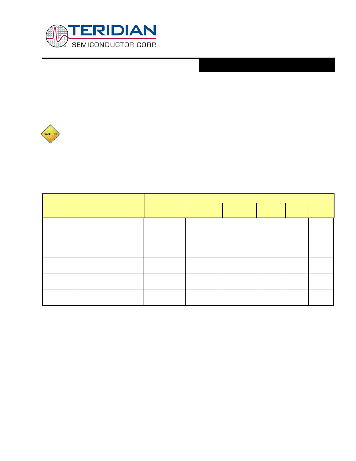
71M6513/71M6513H
3-Phase Energy Meter IC
DATA SHEET
A Maxim Integrated Products Brand
Element Input Mapping
AUGUST 2011
During operation, the MPU is in charge of controlling the multiplexer cycles, for example by inserting an alternate multiplexer
sequence at regular intervals using MUX_ALT. This enables temperature measurement. The polarity of CHOP must be altered
for each sample. It must also alternate for each alternate multiplexer reading.
The MP U must pr o gr am CHOP_EN alternately between 01 and 10 on every CE_BUSY interrupt except for the first CE_BUSY
after an XFER_BUSY interrupt. Note that when XFER_BUSY occurs, it will always be at the same time as a CE_BUSY
interrupt.
Operating CE codes with environment parameters deviating from the values specified by Teridian will lead to
unpredictable results.
CE Calculations
The CE performs the precision computations necessary to accurately measure power. These comput ations include offset
cancellation, phase compensation, product smoothing, product summation, frequency detection, VAR calculation, sag
detection, peak detection, and voltage phase measurement. All data computed by the CE is depen d ent on t h e s el ec t ed m et er
equation as given by EQU (in I/O RAM). As a function of EQU, the element components V0 through I2 take on different
meanings.
EQU
0
1
2
3
4
5
Watt & VAR Formula
(WSUM/VARSUM)
VA I A (1 elem ent, 2W 1φ)
VA*(IA-IB)/2
(1 element, 3W 1φ)
VA*IA + VB*IB
(2 element, 3W 3φ Delta)
VA*(IA-IB)/2 + VC *IC
(2 element, 4W 3φ Delta)
VA*(IA-IB)/2 + VB*(IC-IB)/2
(2 element, 4W 3φ Wye)
VA*IA + VB*IB + VC*IC
(3 element, 4W 3φ Wye)
W0SUM/
VAR0SUM
VA*IA - - IA - -
VA*(IA-IB)/2 - (IA-IB) IB -
VA*IA VB*IB - IA IB -
VA*(IA-IB)/2 - VC*IC IA-IB IB IC
VA*(IA-IB)/2 VB*(IC-IB)/2 - IA-IB IC-IB IC
VA*IA VB*IB VC*IC IA IB IC
W1SUM/
VAR1SUM
W2SUM/
VAR2SUM
CE RAM Locations
The information given in the following tables apply to CE code Version CE13B09D.
I0SQ
SUM
I1SQ
SUM
I2SQ
SUM
Page: 68 of 104 © 2005-2011 Teridian Semiconductor Corporation
Page 69
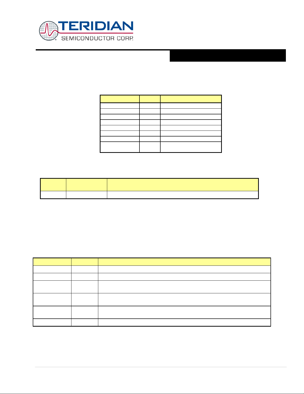
71M6513/71M6513H
3-Phase Energy Meter IC
DATA SHEET
A Maxim Integrated Products Brand
0x00
IA
Pha se A cur rent
0x01
VA
Phase A voltage
0x02
IB
Pha se B cur rent
0x03
VB
Phase B voltage
0x04
IC
Pha se C current
0x05
VC
Phase C voltage
0x06
TEMP
Temperature
V3 monitor/comparator
input
SAG_THR
SAG_CNT
SEPTEMBER 2011
CE Front End Data (Raw Data)
Access to the raw data provided by the AFE is possible by reading addresses 0 through 7, as listed below.
Address (HEX) Name Description
0x07 V3
CE Status Word
Since the CE_BUSY interrupt occurs at 2520.6Hz, it is desirable to minimize the computation required in the interrupt handler
of t he MPU. T he CE status wo rd can b e read by the MPU at ev ery CE_BUSY inter rupt.
CE
Address
0x51 CESTATUS Se e description of CE status word below
The CE Status Word is useful for generating early warnings to the MPU. It contains sag warnings for phase A, B, and C, as
well as F0, the derived clock operating at the fundamental input frequency. CESTATUS provides information about the status of
voltage and input AC signal frequency, which are useful for generating an early power fail warning to initiate necessary data
storage. CESTATUS represe nts the status flags for the prece ding CE code pass (CE_BUSY interrupt).
Note: The CE does not store sag alarms from one code pass to the next. CESTATUS i s ref resh ed at ever y CE_BUS Y
interrupt and remains valid for up to 100 µs after the CE_BUSY interrupt occurs. Unsynchronized read operations of
CESTATUS will yield unreliable results.
The significance of the bits in CESTATUS is shown in the table b elow:
CESTATUS Bit Name Description
31-29 Not Used These unused bits will always be zero.
28 F0 F0 is a square wave at the exact fundamental input frequency.
27 SAG_C
26 SAG_B
25 SAG_A
24-0 Not Used These unused bits will always be zero.
For generating proper status information, the CE is i nitialized by the MPU using SAG_THR (default of 80V RMS at the meter
input if VMAX=600V) and SAG_CNT (default 80 samples). Using the default value for SAG_CNT, the peak-to-peak signal has to
be below SAG_THR value for 32 millisec onds to activate t he SAG_X status bits.
Name Description
Normally zero. Becomes one when |VC| remains below SAG_THR for SAG_CNT
samples. Will not return to zero until |VC| ris es above SAG_THR.
Normall y z ero. B ecomes one wh en |VB| r emains below
samples. Will not return to zero until |VB| ris es above SAG_THR.
Normall y z ero. B ecomes one wh en |VA| r emains below SAG_THR for SAG_CNT
samples. Will not return to zero until |VA} ris es abov e SAG_THR.
for
© 2005-2011 Teridian Semiconductor Corporation Page: 69 of 104
Page 70
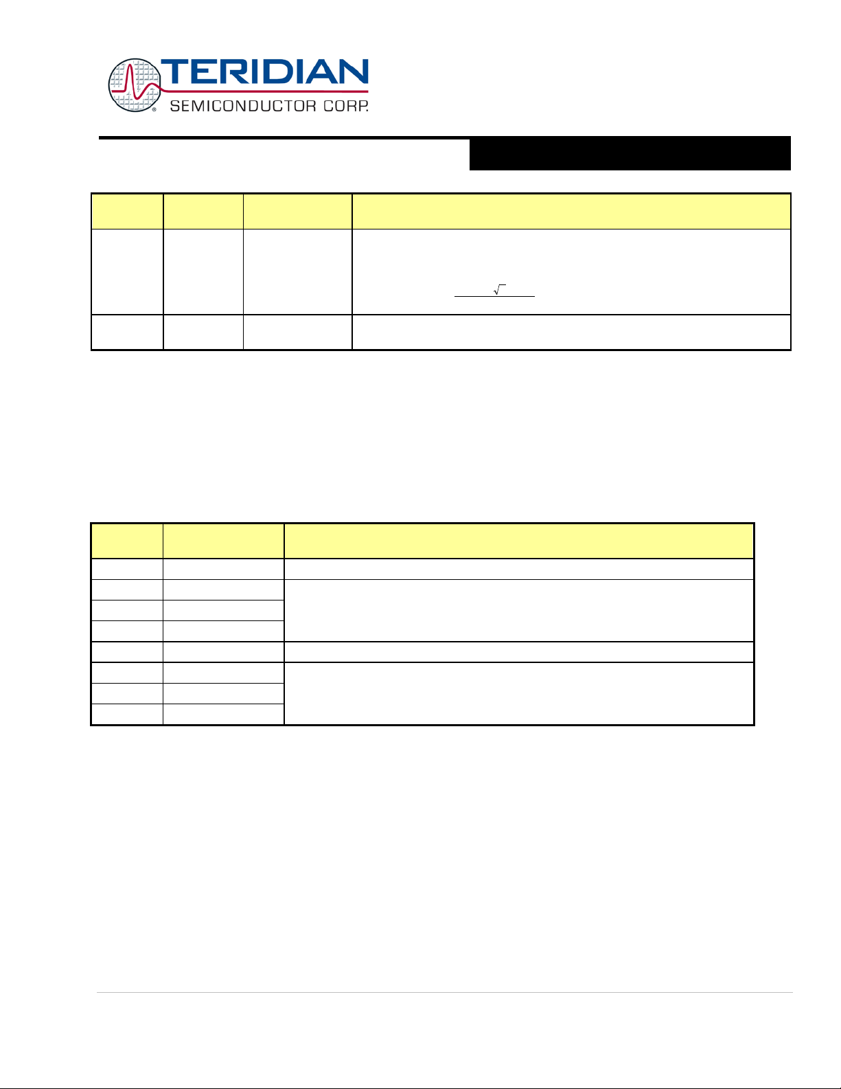
71M6513/71M6513H
3-Phase Energy Meter IC
DATA SHEET
A Maxim Integrated Products Brand
Meter voltage inputs must be above this threshold to prevent sag alarms.
9
108798.7
280
_
−
⋅⋅
=
VMAX
THRSAG
0x42
WSUM_X
The signed sum: W0SUM_X+W1SUM_X+W2SUM_X
W0SUM_X
AUGUST 2011
CE
Address
0x31 SAG_THR
0x32 SAG_CNT 80
Name Default Description
+23,930,000
(0x16D23AA)
LSB = VMAX * 7.879810
For examp le, if a sag threshold of 80V RMS is desired,
Num ber of consec utiv e volta ge samples below SAG_THR before a sag alarm
is declared (80*397µs = 31.8ms).
-9
V.
CE Transfer Variables
Wh en t he M PU r ec ei v es t h e XFER_BUSY interrupt, it knows that fresh data is available in the transfer variables. CE transfer
variables are modified during the CE code pass that ends with an XFER_BUSY interrupt. They remain constant throughout
each accumulation in terval. In t his dat a sheet, the names of CE trans fer var iabl es alw ays end wi th _X.
Fundame ntal Po w er Measureme nt Variable s
The table below describes each transfer variable for fundamental power measurement. All variables are signed 32 bit integers.
Accumulated variables such as WSUM are internally scaled so they have at least 2x margin before overflow when the
integration time is 1 second. Additionally, the hardware will not permit output values to ‘fold back’ upon overflow.
CE
Address
0x43
0x44 W1SUM_X
0x45 W2SUM_X
0x46 VARSUM_X
0x47 VAR0SUM_X
0x48 VAR1SUM_X
0x49 VAR2SUM_X
WSUM_X and VARSUM_X are the signed sum of Phase-A, Phase-B and Phase-C Wh or VARh values according to the
metering equation specified in the I/O RAM register EQU. WxSUM_X is t he Wh val ue accumulated for phase ‘x’ in the last
accumulation interval and can be computed based on the sp ecified LSB v alue.
For examp le, with VMAX = 600V and IMAX = 208A, LSB (for WxSUM_X ) is 0.1173 µWh.
Instantaneous Power Measurement Variables
The FREQSEL Register selects the input phase used for frequency measurement and for the MAIN_EDGE counter. The
frequency measurement is implemented using the frequency locked loop of the CE for the selected phase.
IxSQSUM_X and VxSQSUM are the squared current and voltage samples acquired during the last accumulation interval.
INSQSUM_X can be used for computing the neutral current.
Name Description
The s um of Wa t t sampl es from each wat t meter elem ent.
LSB = 9.4045*10
The signed sum: VAR0SUM_X+VAR1SUM_X+VAR2SUM_X
The s um of VA R samples from each wat t meter elem ent.
LSB = 9.4045*10
-13
VMAX IMAX / In_8 Wh.
-13
VMAX IMAX / In_8 VARh.
Page: 70 of 104 © 2005-2011 Teridian Semiconductor Corporation
Page 71

71M6513/71M6513H
3-Phase Energy Meter IC
DATA SHEET
A Maxim Integrated Products Brand
Selected phase for the frequency monitor, the phase-to-phase voltage
6
32
10587.0
2
−
⋅≈≡
S
F
∑
++
2
210
)( III
V0SQSUM_X
ACC
S
RMS
N
FLSBVxSQSUM
Vx
⋅⋅⋅
=
3600
ACC
S
RMS
N
FLSBIxSQSUM
Ix
⋅⋅⋅
=
3600
SEPTEMBER 2011
CE
Address
0x33 FREQSEL
0x41 FREQ_X
0x4A I0SQSUM_X
0x4B I1SQSUM_X
0x4C I2SQSUM_X
0x4D INSQSUM_X
0x4E
0x4F V1SQSUM_X
0x50 V2SQSUM_X
0x5A V3SQSUM_X
Name Description
measurements, and voltage zero crossings:
Phase A: 0 (default)
Phase B: 1
Phase C: 2
Fundamental frequency. LSB
The s um of squared c urrent samples fr om each element.
LSB = 9.4045*10
The s um of squared c urrent samples fr om the calculated neutral:
LSB = 1.2539*10
The s um of squared v oltage samples fr om each elemen t .
LSB= 9.4045*10
The s um of squared v oltage samples fr om the V3 input. If CAL_V3 =
8192, then LSB = 9.4045*10
-13
IMAX2 / In_82 A2h
.
-12
IMAX2 / In_82 A2h
-13
VMAX2 V2h
-13
VMAX2 V2h or 9. 4045* 10
Hz
-13
IMAX2 I2h
The RMS values can be computed by the MPU from the squared current and voltage samples as per the formulae:
Other Measurement Parameters
PH_AtoB_X and PH_AtoC_X contain phase angle information between the phase voltages, depending on the setting of
FREQ_SEL, as shown in the table below. The phase angle information can be used for phase sequencing and error detection.
If the voltage at the selected phase is missing, the meter accuracy will be reduced.
To m aint ain ac curac y, FREQ_SEL must be set to a phase with an active voltage. For example, in a system where
phase A is lost (which can be detected using the SAG bits or by comparing the voltage VA with a lower limit),
FREQ_SEL must be set to an alt ernative pha se to ma i ntai n accur acy.
MAINEDGE_X is us efu l fo r im pl emen ti ng a r eal -time clock based on the input AC signal. MAINEDGE_X is the number of half-
cycles accounted for in the last accumulated interval for the AC signal of the phase specified in the FREQ_SEL register.
© 2005-2011 Teridian Semiconductor Corporation Page: 71 of 104
Page 72
71M6513/71M6513H
3-Phase Energy Meter IC
DATA SHEET
A Maxim Integrated Products Brand
Description
AUGUST 2011
CE
Address
0x52
0x53
0x55 MAINEDGE_X
Temperature Measurement and Temperature Compensation
Input variables: TEMP_NOM is the reference value for temperature measurement, i.e. when this value is set with
TEMP_RAW_X at known temperature. The 71M6513/6513H measures temperature with reference to this value.
DEGSCALE is the slope or rate of t emperature increa se or d ecrease from the TEMP_NOM for TEMP_X measurement.
PPMC and PPMC2 are temperature compensation coefficients. Their values should reflect the characteristics of the band gap
voltage reference of the chip. PPMC and PPMC2 follow the square law characteristics to compensate for nonl inear temperature
behaviors, when the 71M6513/6513H is in internal temperature compensation mode.
EXT_TEMP al lo ws the MP U t o s elec t b etw een d ir ect con tr ol of GAIN_ADJ or management of GAIN_ADJ by the CE, based on
TEMP_X a nd the t emperature correction coeff i cients PPMC and PPMC2.
Name
PH_AtoB_X
Angle in degrees PH_AtoB_X*360/NACC+2.4 PH_AtoB_X*360/NACC+2.4 PH_AtoB_X*360/NACC-4.8
PH_AtoC_X
Angle in degrees PH_AtoC_X*360/NACC+4.8 PH_AtoC_X *360/NACC-2.4 PH_AtoC_X *360/NACC-2.4
FREQU_SEL = 0 FREQU_SEL = 1 FREQU_SEL = 2
Phase lag from VA to VB. Phase lag from VB to VC. Phase lag from VC to VA.
Phase lag from VA to VC. Phase lag from VB to VA. Phase lag from VC to VB.
The number of zero
crossings of VA in the previous accumulation interval.
Edge crossings are either direction and are debounced.
The number of zero
crossings of VB in the previous accumulation interval.
The number of zero
crossings of VC in the previous accumulation interval.
Page: 72 of 104 © 2005-2011 Teridian Semiconductor Corporation
Page 73

71M6513/71M6513H
3-Phase Energy Meter IC
DATA SHEET
A Maxim Integrated Products Brand
Dur ing calibration, the v alue of TEMP_RAW_X should be placed in
Should be 15 or 0. When 15, causes the CE to ignore internal temperature
⋅
+
⋅
++=
23
2
14
2
2_
2
_
116384_
PPMCXTEMPPPMCXTEMP
floorADJGAIN
Linear temperature compensation factor. Equals the linear temperature co-
the meter to run faster when hot. The compensation factor affects both V and
Square-law temperature compensation factor. Equals the square-law tem-
CE
Address
Filtered, unscaled reading from temperature sensor. This value should be
Scales all voltage and current inputs. 16384 provides unity gain. Default is
SEPTEMBER 2011
CE
Address
0x11 TEMP_NOM 0
0x30 DEGSCALE 22721
0x38 EXT_TEMP 0
0x39 PPMC 0
0x3A PPMC2 0
Name Default Description
TEMP_NOM.
Scale factor for TEMP_X.
TEMP_X = -DEGSCALE*2
compensation and permits the MPU to contr ol GAIN_ADJ. When internal
tem perature compensatio n is sel ected, GAIN_ADJ will be:
Default is 0 (internal compens ation ) .
eff icien t (PPM/°C) of V REF multipl ied by 26.84, or TC1 ( expressed in µV/°C ,
see Electrical Specificat ions) multiplied by 22 . 46
I and will therefore have a double effect on products.
1
CE scaling factor 22.46=221/(1.195*57)
perature coefficient (PPM/°C2) of VREF multiplied by 1374, or TC2 (expressed in µV/° C
sitive value will ca use the meter t o run faster when hot. The compensation
factor affects both V and I and will therefore have a double effect on products.
2
CE scaling factor 1150=229/(1.195*58)
2
-22
*(TEMP_RAW_X-TEMP_NOM).
1
. A positive value will cause
, see Electrical Specification s) mult iplied by 11502.1. A po-
Output variables: TEMP_X is the temperature measurement from reference temperature of TEMP_NOM. TEMP_X is
computed using TEMP_RAW_X and DEGSCALE. T his qua nti ty i s po si ti ve wh en t he t em per at ur e is abo ve t he r efer enc e a nd is
negative for cold temperatures.
TEMP_RAW_X is the raw processed value from ADC output and is the fundamental quantity for tem perature measurement.
TEMP_RAW_X is less than TEMP_NOM at higher temperatures. TEMP_RAW_X is more than TEMP_NOM for cooler
tem peratures than reference tem perature.
GAIN_ADJ is a scaling factor for power measurements based on temperature (when in internal t emperature compensation
mode). In general, for higher temperatures it is lower than 16384 and higher than 16384 for lower temperatures. GAIN_ADJ is
mainly dependent on the PPMC, PPMC2 and TEMP_X r egis ter v alu es. Thi s par amet er i s aut omat ica lly comp uted b y th e CE
and is used by the CE for temperature compensation.
Name Description
0x40 TEMP_X Deviation from Calibrat ion tem perature. LSB = 0.1 0C.
0x54 TEMP_RAW_X
0x2E GAIN_ADJ
© 2005-2011 Teridian Semiconductor Corporation Page: 73 of 104
written to TEMP_NOM during meter calibration.
16384. If EXT_TMP = 0, GAIN_ADJ is updated by the CE.
Page 74

71M6513/71M6513H
3-Phase Energy Meter IC
DATA SHEET
A Maxim Integrated Products Brand
Hz
FWSUMWRATEX
RATE
S
46
2
⋅⋅⋅
=
AUGUST 2011
Pulse Generation
Input variables: The combination of the PULSE_SLOW and PULSE_FAST parameters control the speed of the pulse rate. The
default values of 1 and 1 will m aintain the original pul se rate given by the Kh equation.
WRATE controls the number of pulses that are generated per measured Wh and VARh quantities. The lower WRATE i t is the
sl ower is t he pulse r ate for m easured power qu antity . The m etering c onstant Kh is der ived fr om WRATE as th e amount of
energy measured for each pulse. That is, if Kh = 1Wh/pulse, a power applied to the meter of 120V and 30A results in one
pulse per second. If the load is 240V at 150A, ten pulses per second will be generated.
Control is transferred to the MPU for pulse generation if EXT_PULSE > 0. In this case, the pulse rate is determined by
APULSEW and APULSER. The MPU has to load the source for pulse generation in APULSEW and APULSER to generate p ulses.
Irr esp ect i ve of th e EXT_PULSE, status the output pulse rate controlled by APULSEW and APULSER is im pl em ent ed b y the C E
only. By setting EXT_PULSE > 0, the MPU is providing the source for pulse generation. If EXT_PULSE is negative, W0SUM_X
and VAR0SUM_X are the default pulse generation sources. In this case, creep cannot be controlled since it is an MPU function.
The maximum pulse rate is 3*F
PULSE_WIDTH allows adjustment of the pulse width for compatibility with calibration and other external equipment. The
min imum pulse width po ssibl e is 66. 16µs.
The maximum time jitt er is 1/6 of the MUX cycle period (normally 67μs) and is independent of the number of pulses measured.
Thus, if the pulse generator is monitored for 1 second, the peak jitter is 67ppm. After 10 seconds, the peak jitter is 7ppm. The
aver a g e j it t er i s al w ay s zer o . I f it i s at t em pt ed t o dr i v e ei th er pu l s e g ener a t o r f as t er th a n it s m axi m um rat e, i t w il l sim p l y ou t p ut
at its maximum rate without exhibiting any roll-over characteristics. The act ual pul se rate, usi ng WSUM as an example, is:
= 7.56kHz.
S
Where F
PULSE_FAST (see table below).
= 2520.6Hz (sampling frequency), and X = pulse speed factor derived from CE variables PULSE_SLOW and
S
Page: 74 of 104 © 2005-2011 Teridian Semiconductor Corporation
Page 75
71M6513/71M6513H
3-Phase Energy Meter IC
DATA SHEET
A Maxim Integrated Products Brand
When PULSE_SLOW > 0, the pulse generator input is reduced 64x.
X
PULSE_SLOW
PULSE_FAST
-4
0x2D
WRATE
683
Kh =
*66.1782 / (
*WRATE*N
*X) Wh/pulse.
SUM_PRE
PRE_SAMPS
SUM_CYCLES
Wh pulse generator input, to be updated by the MPU when using external pulse
SEPTEMBER 2011
CE
Address
0x28
0x29 PULSE_FAST 1
0x36
0x37 EXT_PULSE 15
0x3C PULSE_WIDTH 50
0x26 APULSEW 0
0x27 APULSER 0
Name Default Description
PULSE_SLOW
1
2520
When PULSE_FAST > 0, the pulse generator input is incr eased 16x.
Thes e two parameters c ontrol the pulse gain factor X (see table below).
Allowed values are either 1 or –1.
1.5 * 22 = 6 -1 -1
1.5 * 26 = 96 -1 1
1.5 * 2
1.5 1 (default) 1 (default)
VMAX*IMAX
Should be 15 or 0. When zero, causes the pulse generators to respond to
WSUM_X and VARSUM_X. Otherwi se, th e genera tors respo nd to values the
MPU places in APULSEW and APULSER.
The maximum pulse width (low-going pulse) is:
(2 * PULSE_WIDTH + 1) * 66 µ s. 0 is a legitimate value.
generation (see DIO_PW bit ). The output pulse rate i s :
APULSEW * F
This input is buffered and can be updated by the MPU during a computation
interv al . The ch ange wi ll take effect at the begi nning of the next int erval .
VARh pulse generator input, to be updated by the MPU when using external
pulse generation (see DIO_PV bit). The output pul se rate is:
APULSER * F
This input is buffered and can be updated by the MPU during a computati on
interv al . The ch ange wi ll take effect at the begi nning of the next int erval .
= 0.09375 1 -1
*
* 2
S
*2
S
-32
* WRATE * 2
-32
* WRATE * 2
(N
In_8
ACC
-14
-14
)
ACC
© 2005-2011 Teridian Semiconductor Corporation Page: 75 of 104
Page 76

71M6513/71M6513H
3-Phase Energy Meter IC
DATA SHEET
A Maxim Integrated Products Brand
Address
0x0B
CAL_VB
16384
CAL_IC
0x65
CAL_V3
8192
Gain cont rol for V3 channel, used for neutral current measurement.
These three constants control the CT phase compensation. No compensation
is increased, more compensation
1. If it is desired to delay the current by the
Φ⋅−
Φ⋅
=
TAN
TAN
XPHADJ
0131.01487.0
02229.0
2_
20
Φ⋅−
Φ⋅
=
TAN
TAN
XPHADJ
009695.01241.0
0155.0
2_
20
During calibration, the value of TEMP_RAW_X should be placed in
CE Ca libr ation P arameters
The table b elow lists the parameters that are ty pical ly ent ered to effect calib ration of meter accurac y .
AUGUST 2011
CE
0x08 CAL_IA 16384
0x09 CAL_VA 16384
0x0A CAL_IB 16384
0x0C
0x0D CAL_VC 16384
0x0E PHADJ_A 0
0x0F PHADJ_B 0
0x10 PHADJ_C 0
0x11 TEMP_NOM N/A
Name Default Description
16384
These constants control the gain of their respective channels. The nominal
value for each parameter is 2
proportional to its C AL parameter . Thus, i f the gain of a channel is 1% slow,
CAL should be increased by 1%.
occurs when PHADJ_X = 0. As PHADJ_X
(lag) is introduced. Range: ±215 –
angle Φ:
TEMP_NOM.
14
= 16384. The gain of ea ch channel is directly
at 60Hz
at 50Hz
Page: 76 of 104 © 2005-2011 Teridian Semiconductor Corporation
Page 77
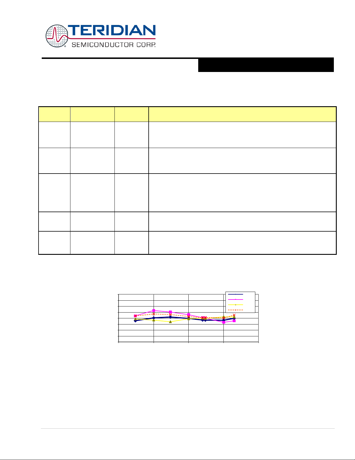
71M6513/71M6513H
3-Phase Energy Meter IC
DATA SHEET
A Maxim Integrated Products Brand
0 Deg
60 Deg
-60 Deg
180 Deg
SEPTEMBER 2011
Ot her CE Paramet ers
The t ab le b elo w sh ows C E par am et ers u sed for sup pr essi on o f noi se d ue t o sc ali ng and t run cat i on ef fec ts a s wel l a s sc ali ng
factors.
CE
Address
Name Default Description
0x2F QUANT 0
0x34 QUANT_VAR 0
0x35 QUANT_I 0
0x3B KVAR 6448
0x64 QUANT_V3 0
TYPICAL PERFORMANCE DATA
Wh Accuracy at Room Temperatu re
This parameter is added to the Watt calculation to compensate for input noise
and truncation.
LSB=(VMAX*IMAX / In_8) *1.04173*10
-9
W
This parameter is added to the VAR calculation to compensate for input noise
and truncation.
LSB = (VMAX*IMAX/In_8) * 1.04173*10
This parameter is added to compensate for input noise and truncation in the
squaring calculations for I
LSB=VMAX
LSB= ( IMAX
2
and V2.
2
*1.04173*10-9 V2
2
/In_82)*1.04173*10-9 A2
-9
W
Scale factor for the VAR calculation. The default value of KVAR sh ould never
need to be changed.
Offse t for low-current measurement on V3.
LSB = = 9.4045*10
-13
IMAX2 A2h
0.2
0.15
0.1
0.05
0
%Error
-0.05
-0.1
-0.15
-0.2
0.1 1 10 100 1000
© 2005-2011 Teridian Semiconductor Corporation Page: 77 of 104
1
0.3
3
10
30
25
A
100
Figure 24: Wh Accuracy, 0.3A - 200A/240V
VARh Accuracy at Room Temperature
200
Page 78
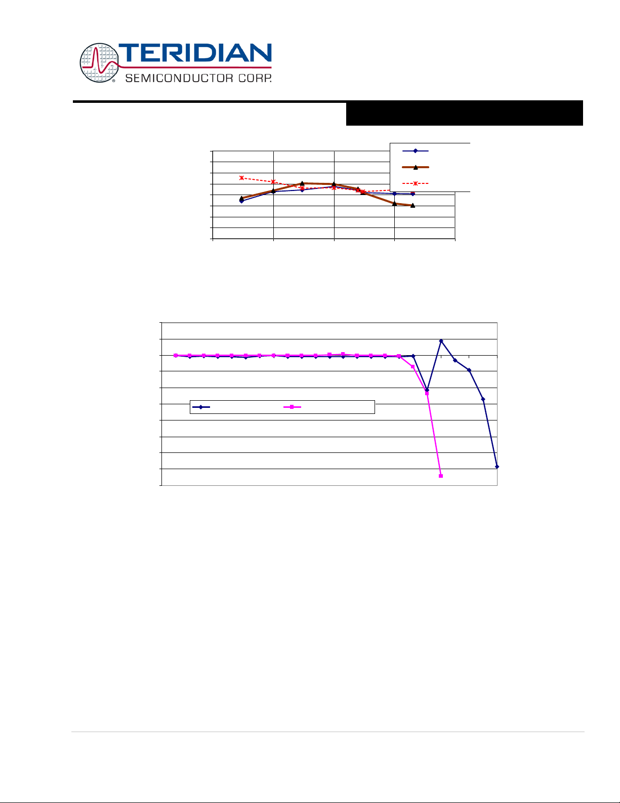
71M6513/71M6513H
3-Phase Energy Meter IC
DATA SHEET
A Maxim Integrated Products Brand
90 Deg
150 Deg
270 Deg
-8
-7
-6
-5
-4
-3
-2
-1
0
1
2
1 3 5 7 9 11 13 15 17 19 21 23 25
Harmonic
Error [ %]
50Hz Har monic Dat a 60Hz Harmonic Data
0.2
0.15
0.1
0.05
0
% Error
-0.05
-0.1
-0.15
-0.2
0.1 1 10 100 1000
0.3
Figure 25: VARh Accuracy for 0.3A to 200A/240V Performance
Harmonic Performan ce
3
1
10
25
30
100
200
A
AUGUST 2011
Test performed at current distortion amplitude of 40% and v olt ag e di stortion am pl i tu d e of 1 0% as p er IEC 62053, part 22 .
Figure 26: Meter Accuracy over Harmonics at 240V, 30A
Page: 78 of 104 © 2005-2011 Teridian Semiconductor Corporation
Page 79
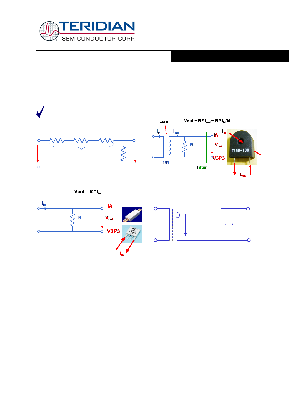
71M6513/71M6513H
3-Phase Energy Meter IC
DATA SHEET
A Maxim Integrated Products Brand
VA = Vin * R
out
/(R
out
+ Rin)
V
in
R
in
R
out
VA
Vout = dI
in
/dt
V
out
R
1/N
I
in
V
C
V3P3
IA
Vout = dI
in
/dt
V
out
R
SEPTEMBER 2011
APPLICATION IN F O R MATION
Connec tion of Sensors ( CT, Resistive Shunt, Rogo ws k i C oil)
Figures 27 through 30 show how resistive dividers, current transformers, restive shunts, and Rogowski coils are connected to
the voltage and current inputs of the 71M6513.
The analog input pins of the 71M6511 are designed for sensors with low source impedance. RC filters with resistance
values higher than those implemented in the Teridian Dem o Boards should be avoided.
Figure 27: Resistive Voltage Divider (left), Current Transformer (right)
Figure 28: Resistive Shunt (left), Rogowski Coil (right)
Distinction between 71M6513 and 71M6513H Parts
71M6513H parts go through a process of trimming and characterization during production that make them suitable to highaccuracy applications.
The first process applied to the 71M6513H is the trimming of the reference voltage, which is guaranteed to have accuracy over
tem perature of better that ±10PPM/°C.
The second process applied to the 71M6513H is the characterization of the reference voltage over temperature. The
coefficients for the reference voltage are stored in so-c al led tr im fu ses ( I/ O RA M r egi st ers TRIMBGA, TRIMBGB, TRIMM[2:0].
The MPU program can read these trim fuses and calculate the correction coefficients PPM1 and PPM2 per the formul ae given
in the Performa nce Specifications sec tion (VREF, V B IAS). S ee the Temper ature C ompensation section for details.
The fuse TRIMBGB is non-zero for the 71M6513H part and zero for the 71M6513 part.
Trim fuse information is not available for non-H parts . Thus , t he standard settings ar e to be ap plied . These s ettin gs are:
• PPMC = TC1 * 22.46 = –149
• PPMC2 = TC2 * 1150.1 = –392
© 2005-2011 Teridian Semiconductor Corporation Page: 79 of 104
Page 80
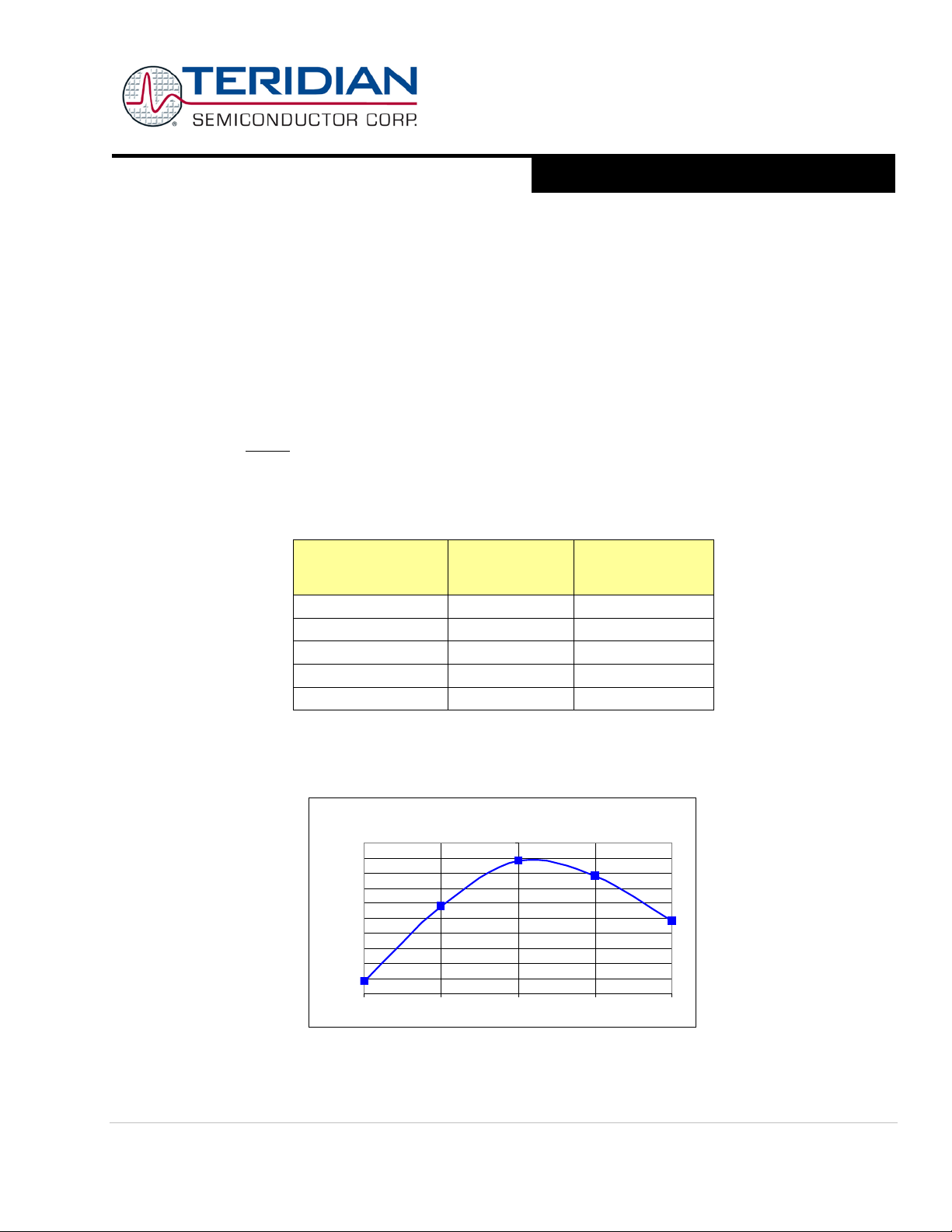
71M6513/71M6513H
3-Phase Energy Meter IC
DATA SHEET
A Maxim Integrated Products Brand
t
µs
f
6
10
32768=
+50
32767.98
-0.61
32767.5
32767.6
32767.7
32767.8
32767.9
32768
32768.1
32768.2
32768.3
32768.4
32768.5
-50 -25 0 25 50
AUGUST 2011
Temperature Compensation and Mains Frequency Stabilization for the RTC
The accuracy of the RTC depends on the stability of the external crystal. Crystals vary in terms of initial accuracy as well as in
terms of behavior over temperature. The flexibility provided by the MPU allows for compensation of the RTC using the substr ate t emp erat ure. To ac hiev e thi s, the cr yst al ha s to be characterized over temperature and the three coefficients Y_CAL,
Y_CALC, and Y_CAL_C2 h ave to be ca lcul ated . Pro vid ed the I C su bstr ate t emper at ures t rac ks th e crys tal temp erat ure, the
coefficients can be used in the MPU firmware to trigger occasional corrections of the RTC seconds count, using the
RTC_DEC_SEC or RTC_INC_SEC registers in I/O RAM.
It is not recommended to measure crystal frequency directly due to the error introduced by the measurement probes. A
practical method to measure the crystal frequency (when installed on the PCB with the 71M6513) is to have a DIO pin toggle
every second, based on the RTC interrupt, with all other interrupts disabled. When this signal is measured with a precision
timer, the crystal frequency can be obtained from the measured time period t (in µs):
Example: Let us assume a crystal characterized by the measurements shown in Table 61. The values show that even at
nominal temperature (the temperature at which the chip was calibrated for energy), the deviation from the ideal crystal
frequency is 11.6 PPM, resulting in about one second inaccuracy per day, i.e. more than some standards allow.
Deviation from
Nominal
Temperature [°C]
+25 32768.28 8.545
0 32768.38 11.597
-25 32768.08 2.441
-50 32767.58 -12.817
Table 61: Frequency over Temperature
As Figure 29 s hows, even a constant compensation would not bring much improvement, since the temperature characteristics
of the crystal are a mix of constant, linear, and quadratic effects (in commercially available crystals, the constant and quadratic
eff ects are dominant).
Measured
Frequency [Hz]
Deviation from
Nominal
Frequency [PPM]
The temperature characteristics of the crystal are obtained from t he curve in Figure 29 by curve-fitting the PPM deviations. A
fairly close curve fit is ac hieved w ith t he coeff ici ents a = 10 . 89, b = 0.122, a nd c = –0.00714 ( see Figure 30).
Page: 80 of 104 © 2005-2011 Teridian Semiconductor Corporation
Figure 29: Crystal Frequency over Temperature
Page 81
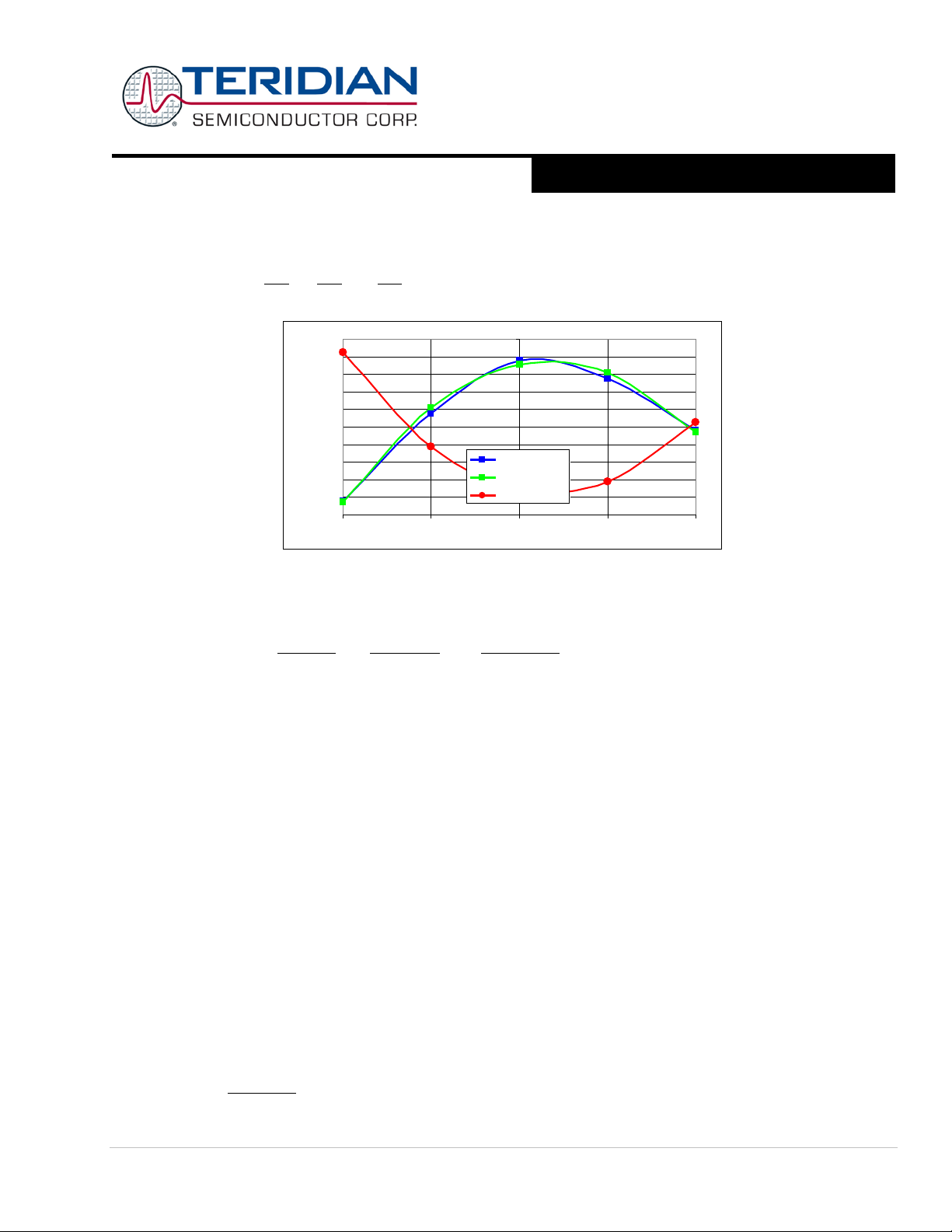
71M6513/71M6513H
3-Phase Energy Meter IC
DATA SHEET
A Maxim Integrated Products Brand
+++⋅=
6
2
66
101010
1
c
T
b
T
a
ff
nom
1000
2_
100
_
10
_
)(
2
CALCY
T
CALCY
T
CALY
ppmCORRECTION ⋅+⋅+=
32767.5
32767.6
32767.7
32767.8
32767.9
32768
32768.1
32768.2
32768.3
32768.4
32768.5
-50 -25 0 25 50
crystal
curve fit
inverse curve
10
_ XTEMP
TT
N
+=
SEPTEMBER 2011
When applying the inverted coefficients, a curve (see Figure 30) will result that effectively neutralizes the original crystal
characteristics. The frequencies were calculated using the fit coeffici ents as follows:
Figure 30: Crystal Compensation
The MPU Demo Code supplied with the Teridian Demo Kits has a direct interface for these coefficients and it directly controls
the RTC_DEC_SEC or RTC_INC_SEC registers. The Demo Code uses the coefficients in the following form:
Not e th at t he c oef fi cien ts are s cal ed by 10, 100, and 1000 to provide more resolution. For our example case, the coefficients
would th en become (after rounding , sinc e the Demo Code a ccepts only i ntegers):
Y_CAL = 109, Y_CALC = 12, Y_CALC2 = 7
Alternatively, the mains frequency may be used to stabilize or check the function of the RTC. For this purpose, the CE
provides a count of the zero crossings detected for the selected line voltage in t he MAIN_EDGE_X address. This count is
equivalent to twice the line frequency, and can be used to synchronize and/or correct the RTC.
In a production electricity meter, the 71M6513 or 71M6513H is not the only component contributing to temperature dependency. In fact, a whole range of components (e.g. current transformers, resistor dividers, power sources, filter capacitors)
will exhibit slight or pronounced temperature effects. Since the output of t he on-chip t emper at ure s ens or i s ac ces si bl e to th e
MPU, temperature-compen satio n m echani sms with great fl exibi lity, i .e. bey ond the capabilities implem ented in the CE, are
possible.
Temperature measurement can be implemented with the following steps:
1) At a known temperature T
2) Read the TEMP_X r egist er at th e known t emperature. The obtain ed value should be <±0.1°C.
3) The temperature T (in °C) at any environment can be obtained by reading TEMP_X and applying the following
formula:
© 2005-2011 Teridian Semiconductor Corporation Page: 81 of 104
, read the TEMP_RAW regist er of the CE and write the value into TEMP_NOM.
N
External Temperature Compensation
Temperature Measurement
Page 82
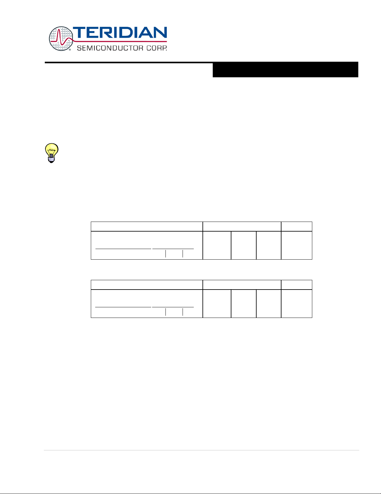
71M6513/71M6513H
3-Phase Energy Meter IC
DATA SHEET
A Maxim Integrated Products Brand
T
VREF(T) deviation from VNOM(T)
)40,22max(
10
)(
)()(
6
−−TTVNOM
TVNOMTVREF
Parameter
Min
Typ
)40,22max(
10
)(
)()(
6
−−TTVNOM
TVNOMTVREF
AUGUST 2011
Temperature Compensation
For the 71M6513 (regular accuracy parts), the temperature coefficients TC1 and TC2 are given as constants t hat represent
typical component behavior (in µV/°C
PPM/°C.
For the high-accuracy parts, individualized coefficients TC1 and TC2 can be retrieved from the on-chip fuses via TRIMBGA,
TRIMBGB, TRIMM[2:0] (see Section ‘Distinction between 71M6513 and 71M6513H Parts’). For the 71M6513H, TC1 and TC2
allow compensation for variations of the reference voltage to within ±10 PPM/°C
Since TC1 a nd TC2 are given in µV/°C and µV/°C
taken into account when transitioning to PPM/°C and PPM/°C
PPMC2 = 1374*TC2/1.195).
Close exam inat ion of t he electrical spec ific ation ( see Table 62) for the 71M6513 reveals t hat the achievable d eviat ion is not
strictly ±40 PPM/°C over the whole temperature range: Only for temperatures for which T-22 > 4 0 ( i.e. T > 62°C) or for whi ch
T-22 < -40 (i.e. T < -18°C), t he data s heet states ±40 PPM/° C. For temperatures between -18°C and +62°C, the error should
be considered constant at ±1,600 PPM, or ±0.16%.
Similar considerations apply to the high-accuracy part 71M6513H (see Table 63), where the err or aroun d the cal ibration
temperature should be considered constant at ±600 PPM, or ±0.06%.
Table 62: VREF Definition for the Re gular A ccura cy Part s 71M6513
2
). TC1 and TC2 allow compensation for variations of the reference voltage to withi n ±40
2
, respectively, the value of the VREF voltage (1.195V) has to be
2
. This means that PPMC = 26.84*TC1/1.195 and
Parameter Min
-40 +40 PPM/ºC
Table 63: VREF Definition for the High-Accuracy Parts 71M6513H
yp
VREF(T) deviation from VNOM(T)
-10 +10 PPM/ºC
Figure 31 and Figure 32 show this concept graphically. The “box” from -18°C to +62°C reflects the fact that it is impractical
to measure the temperature coefficient of high-quality refer ences at smal l temperature excu rsi ons. Fo r example, at +25°C,
the expected err or wou ld be ±3°C * 40 PPM/°C, or just 0.012% for the regular-accuracy parts.
The maximum deviation of ±2520 PPM (or 0.252%) for the regular-accuracy parts is reached at the temperature
extremes. If the reference voltage is used to measure both voltage and current, the identical errors of ±0.252% add up to
a maximum W h registration error of ±0.504%.
The maximum deviation of ±630 PPM (or 0.063%) for th e 71M6513H is reached at the temperature extremes. If the
reference voltage is used to measure both voltage and current, the identical errors of ±0.063% add up to a maximum Wh
registration error of ±0.126%.
Page: 82 of 104 © 2005-2011 Teridian Semiconductor Corporation
Page 83
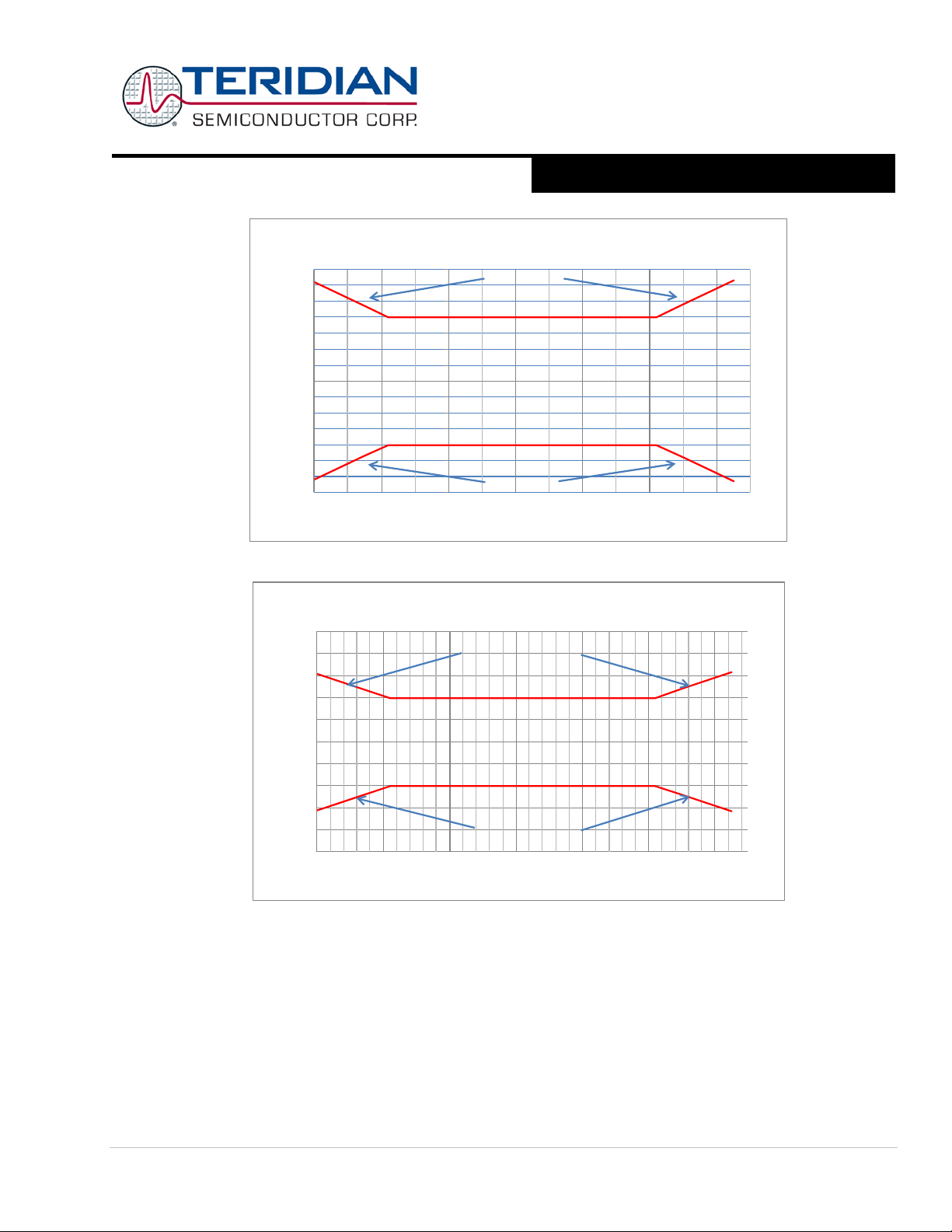
71M6513/71M6513H
3-Phase Energy Meter IC
DATA SHEET
A Maxim Integrated Products Brand
-2800
-2400
-2000
-1600
-1200
-800
-400
0
400
800
1200
1600
2000
2400
2800
-40 -20 0 20 40 60 80
Error Band (PPM) over Temperature (°C)
±40 PPM/°C
±40 PPM/°C
-1000
-800
-600
-400
-200
0
200
400
600
800
1000
-40 -20 0 20 40 60 80
Error Band (PPM) over Temperature (°C)
-10 PPM/°C
+10 PPM/°C
Figure 31: Error Band for VREF over Temperature (Regular-Accuracy Parts)
SEPTEMBER 2011
Figure 32: Error Band for VREF over Temperature (High-Accuracy Parts)
The oscillator drives a standard 32.768 kHz watch crystal. The oscillator has been designed specifically to handle t hese
crystal s a nd i s com pati ble with t h eir hi gh impedance a nd l im i ted p ow er ha ndlin g c apabi li ty. The oscillator power dissipation is
very low to maximize the lifetime of any battery backup device attached to VBAT.
Board layouts with minimum capacitance from XIN to XOUT will require less battery current. Good layouts will have XIN and
XOU T shiel ded from each other.
© 2005-2011 Teridian Semiconductor Corporation Page: 83 of 104
Crystal Oscillat or
Page 84
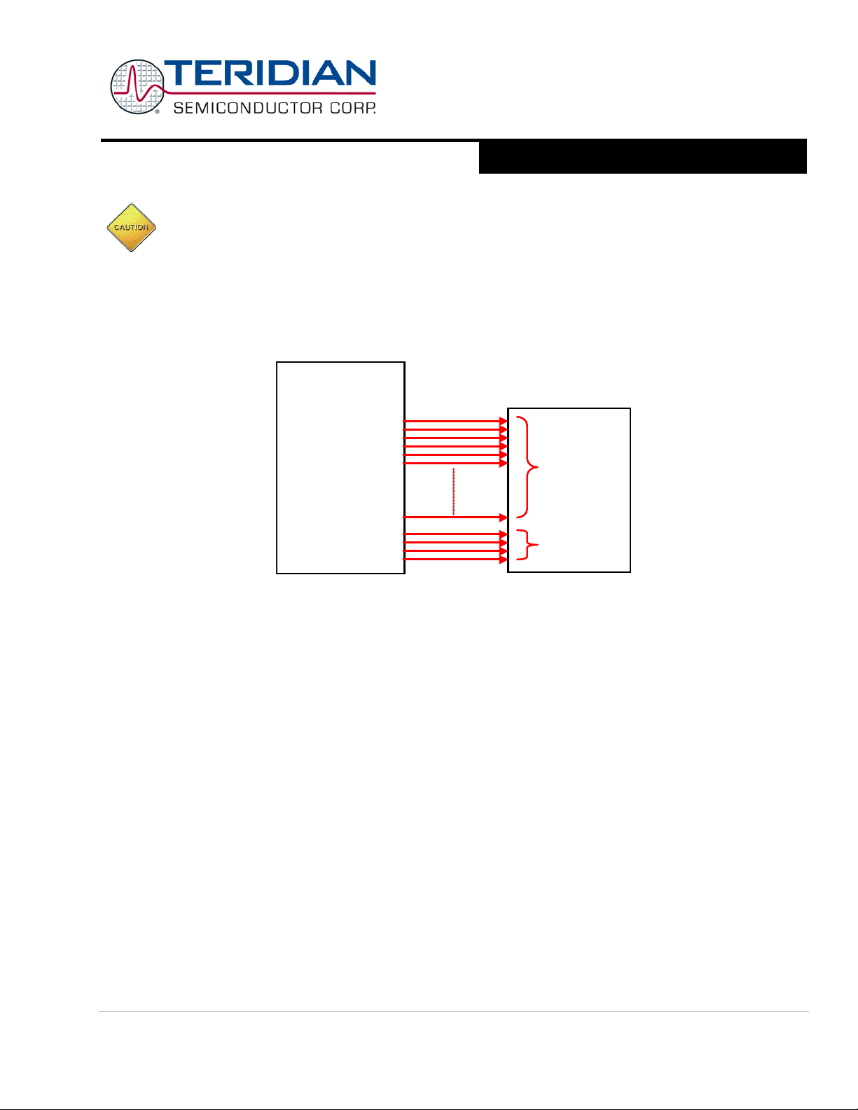
71M6513/71M6513H
3-Phase Energy Meter IC
DATA SHEET
A Maxim Integrated Products Brand
segments
71M6513
LCD
commons
segments
71M6513
LCD
commons
AUGUST 2011
For best rej ecti on of electromagnetic interference, connect the crystal body and the ground terminals of the two
crystal capacitors to GNDD through a ferrite bead. No external resistor should be connected across the crystal,
since the oscillator is self-biasing.
Connec ting LCDs
The 71M6513 has a LCD controller on-chip capable of controlling static or multiplexed LCDs. Figure 33 shows the basic
connection for a LCD.
Figure 33: Connecting LCDs
Figure 34 shows how 5V LCDs can be operated even when a 5V supply is not available. Setting the I/O RAM register
LCD_BSTEN t o 1 starts the on-chip boost circuitry that will output an AC frequency on the VDRV pin. Using a small coupling
capacitor, two general-purpose diodes and a reservoir capacitor, a 5VDC voltage is generated which can be fed back into the
VLCD pin of the 71M6513. The LCD drivers are enabled with the I/O register LCD_ON; I/O register LCD_FS is used to adjust
contrast, and LCD_MODE selects the operation mode (LCD type).
Page: 84 of 104 © 2005-2011 Teridian Semiconductor Corporation
Page 85
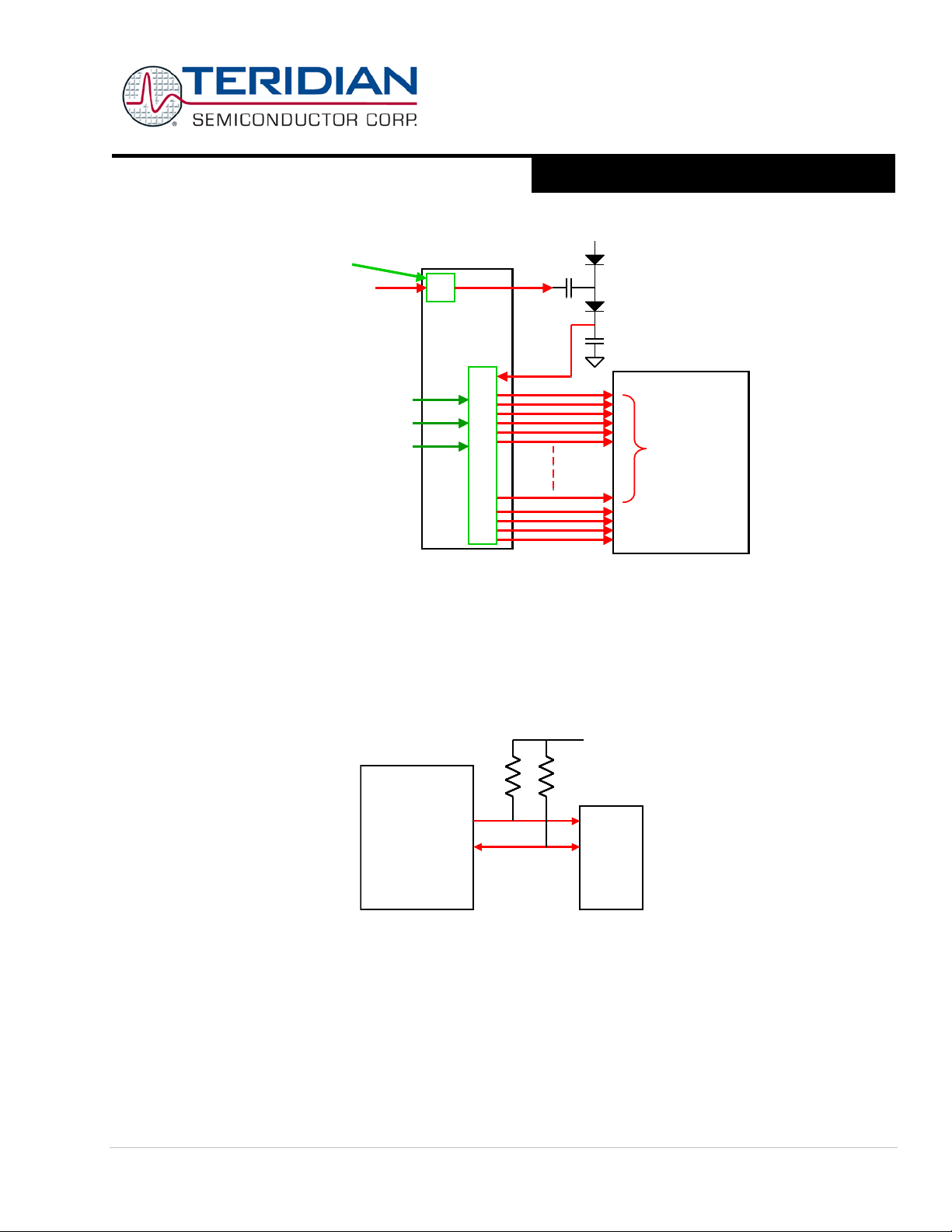
71M6513/71M6513H
3-Phase Energy Meter IC
DATA SHEET
A Maxim Integrated Products Brand
LCD_BSTEN
segments
71M6513
5V LCD
commons
VLCD
V3P3
5VDC
VDRV
V3P3
LCD_FS
LCD_EN
LCD_MODE
Contrast
ON/OFF
LCD type
LCD_BSTEN
segments
71M6513
5V LCD
commons
VLCD
V3P3
5VDC
VDRV
V3P3
LCD_FS
LCD_EN
LCD_MODE
Contrast
ON/OFF
LCD type
DIO4
DIO5
71M6513
EEPROM
SCL
SDA
V3P3
3kΩ
3kΩ
DIO4
DIO5
71M6513
EEPROM
SCL
SDA
V3P3
3kΩ
3kΩ
SEPTEMBER 2011
Figure 34: LCD Boost Circuit
I2C EEPROMs or other I2C compatible devices should be connected to the DIO pins DIO4 and DIO5, as shown in Figure 35.
Pull-up resistors of roughly 3kΩ t o V3P3 should be used for both SCL and SDA signals. The DIO_EEX register in I/O RAM
must be set to 1 in order to convert the DIO pins DIO4 and DIO5 to I2C pins SCL and SDA.
In general, all pins of the 71M6513 are compatible with external 5V devices. The exceptions are the power supply pins and the
RX pin of th e UART (see sect ion Electrical S pecificati ons).
© 2005-2011 Teridian Semiconductor Corporation Page: 85 of 104
Connecting I2C EEPROMs
Figure 35: EEPROM Connection
Connecting 5V Devices
Page 86
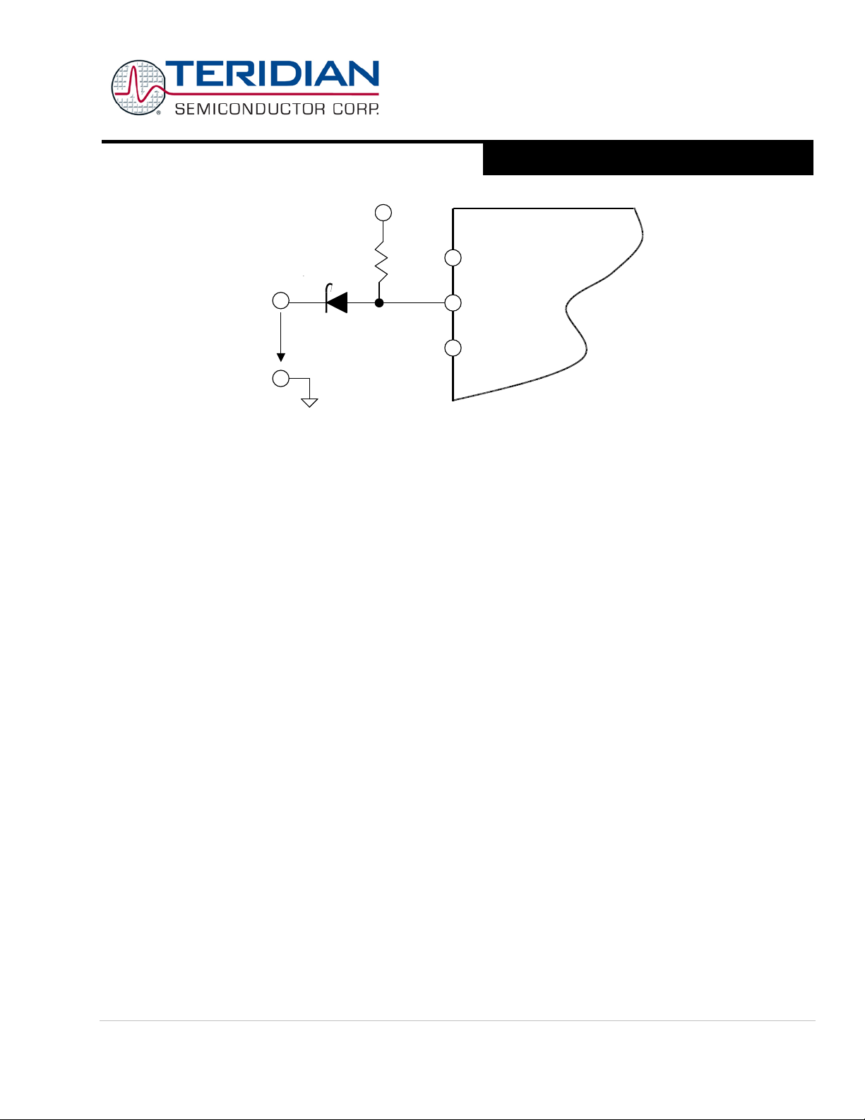
71M6513/71M6513H
3-Phase Energy Meter IC
DATA SHEET
A Maxim Integrated Products Brand
71M651X
VIN
RX
R1 = 100kΩ
V3P3
Figure 36: Interfacing RX to a 0-5V Signal
Figure 36 shows how a 5V signal from an external device can be safely interfaced to the RX pin.
AUGUST 2011
Page: 86 of 104 © 2005-2011 Teridian Semiconductor Corporation
Page 87
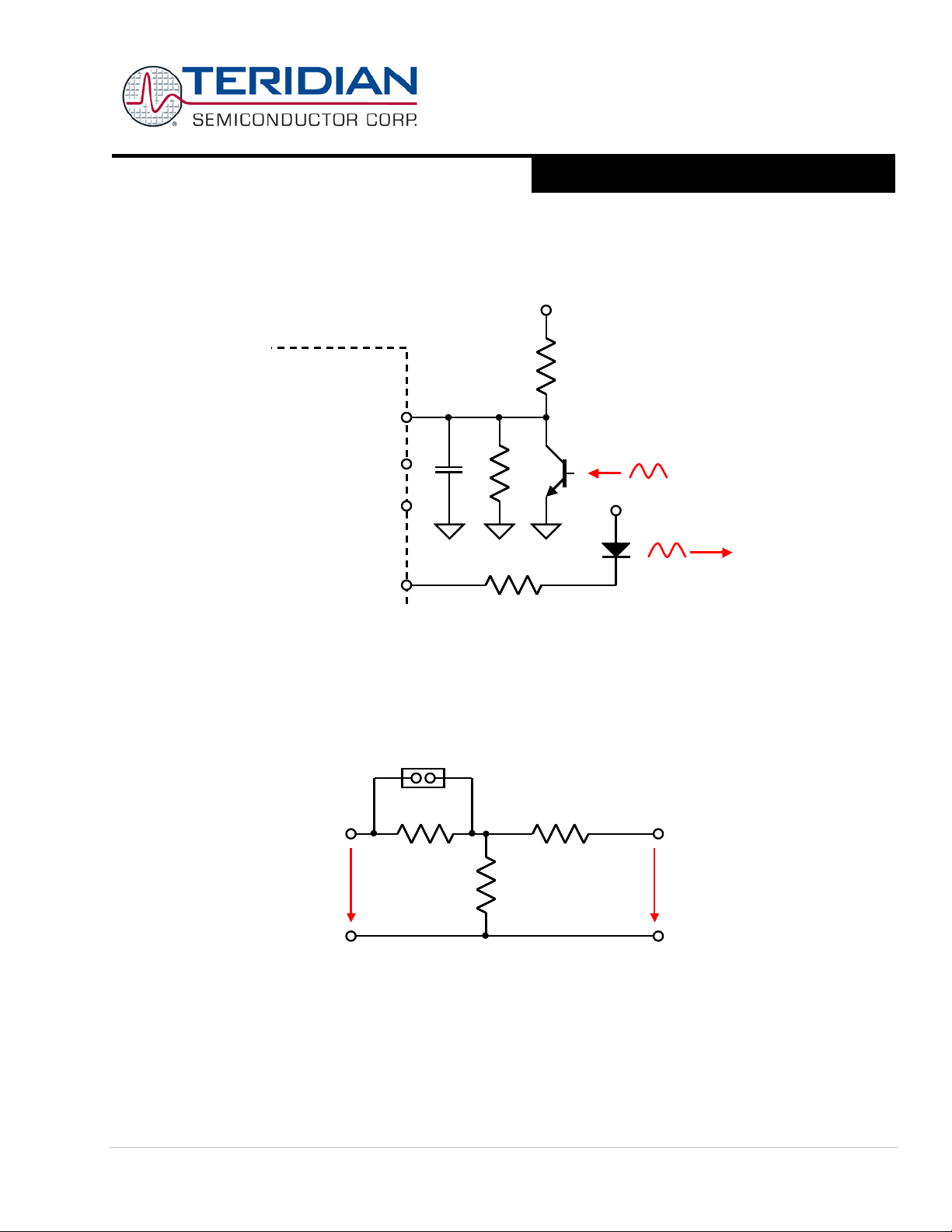
71M6513/71M6513H
3-Phase Energy Meter IC
DATA SHEET
A Maxim Integrated Products Brand
OPT_TX
R
2
R
1
OPT_RX
71M6513
V3P3SYS
Phototransistor
LED
100kΩ
100pF
V3P3SYS
OPT_TX
R
2
R
1
OPT_RX
71M6513
V3P3SYS
Phototransistor
LED
100kΩ
100pF
V3P3SYS
V
in
R
2
V1
R
1
R
3
10kΩ
V
in
R
2
V1
R
1
R
3
10kΩ
SEPTEMBER 2011
Optical Interface
The pins OPT_TX and OPT_RX can be used for a regular serial interface, e.g. by connecting a RS_232 transceiver, or they
can be used to directly operate optical components, e.g. an infrared diode and phototransistor implem enting a FLAG interface.
Figure 37 shows the basic connections. The OPT_TX pin becomes active when the I/O RAM register OPT_TXDIS is set to 0.
Figure 37: Con nection for Optical Components
Connecting V1 and Reset Pin s
A voltage divider should be used to establish that V1 is in a safe range when the meter is in mission mode (V1 must be lower
than 2.9V in all cases in order to keep the hardware watchdog timer enabled). For proper debugging or loading code into the
71M6513 mounted on a PCB, it is necessary to have a provision like the header shown above R1 in Figure 38. A shorting
jumper on this header pulls V1 up to V3P3 disabling the hardware watchdog timer.
Figure 38: Voltage Divider for V1
Even though a functional meter will not necessarily need a reset switc h, it is useful to have a reset pushbutton for prototyping.
When a circuit is used in an EMI environm ent, the RESETZ pin should be supported by the external components shown in
Figure 39. R
be mounted as close as possible to the IC. In cases where the trace from the pushbutton switch to the RESTZ pin poses a
problem, R
should be in the range of 200Ω, R2 should be around 10Ω. The capacitor C1 should be 1nF. R1 and C1 should
1
can be removed.
2
© 2005-2011 Teridian Semiconductor Corporation Page: 87 of 104
Page 88
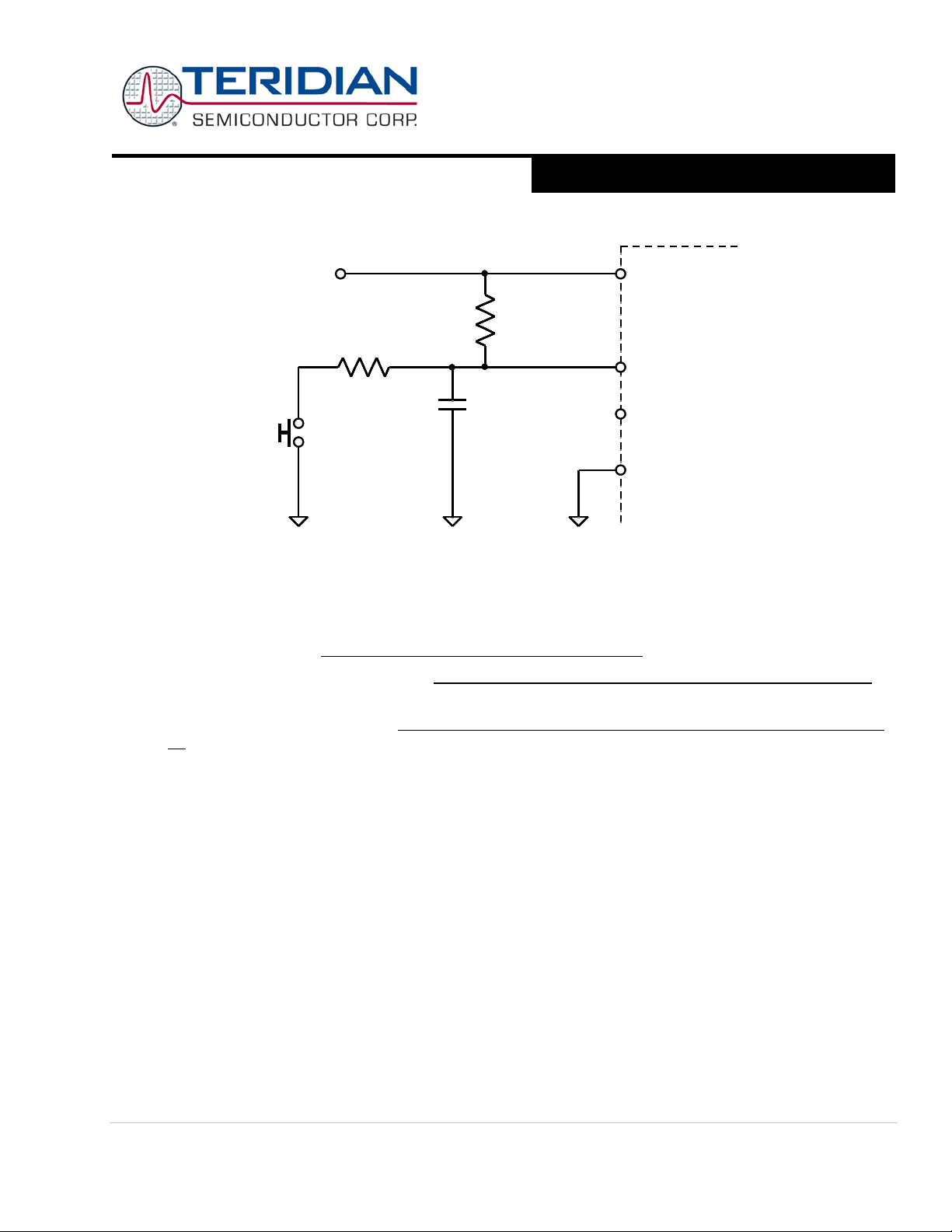
71M6513/71M6513H
3-Phase Energy Meter IC
DATA SHEET
A Maxim Integrated Products Brand
R
1
RESETZ
71M6513
DGND
V3P3
R
2
V3P3
Pushbutton
C
1
200Ω
1nF
10Ω
R
1
RESETZ
71M6513
DGND
V3P3
R
2
V3P3
Pushbutton
C
1
200Ω
1nF
10Ω
AUGUST 2011
Figure 39: External Components for RESETZ
Connecting the V3 Pin
The following should be noted when connecting the V3 pin:
1) If the V3 pin is un used it should be left floating or terminated to the VREF pin.
2) If the V3 pin is used as a comparator input the digital input voltage applied to V3 should be limited to VBIAS ±0.9V.
3) If the V3 pin is used either as an auxiliary analog input, and temperature measurements are made and evaluated
using the alternate multiplexer cycle, the V3 input voltage range must be restri cted to VB IA S ±0.9 V (i.e . 0 . 6 V to 2.4
Otherwise, the TEMP or V3 measurement could be inaccurate. This precaution is particularly important for
V).
customers who are using the TEMP samples for temperature compensation, especially with the 71M6513H devices.
Connecting a Battery
Many meter manufacturers assemble the meter PCB with the 71M6513 IC and the other electronic components first and then
join the meter PCB with the meter enclosure, sensors and other main components separately at a later production step.
Typ ically, pr ogramming, final t est (ATE), and calibration ar e perfor med after this seco nd step .
The following production sequence is strongly recommended:
1) During PCB assembly, when adding/inserting the battery, the board supply voltage (V3P3A, V3P3D) should be active
(i.e. at 3.3 VDC), which can be achieved by briefly connecting the battery to V3P3A/V3P3D through a jumper wire.
After the battery is inserted with the board power active, the jumper wire should be removed.
2) The battery should then remain connected throug h fact ory test (ATE), tim e on the sh elf and shipment.
In cases where it is not feasible to power V3P3A/V3P3D while inserting the battery, it is recommended to isolate the battery in
its holder using a removable piece of Kapton tape or other isolating m aterial. This isolation should then be removed once the
meter is fully p owered during the calibration and test proce ss.
Page: 88 of 104 © 2005-2011 Teridian Semiconductor Corporation
Page 89

71M6513/71M6513H
3-Phase Energy Meter IC
DATA SHEET
A Maxim Integrated Products Brand
SEPTEMBER 2011
Flash Programming
Operational or test code can be programmed into the flash m emory using either an in-circuit emulator or the Flash Download
Board Module (FDBM) available from Teridian. The flash programming procedure uses the E_RTS, E_RXTX, and E_TCLK
pins.
MPU Firmware Library
All application-specific MPU functions mentioned above under “Application Information” are available from Teridian as a
standard ANSI C library and as ANSI “C” source code. The code is available as part of the Demonstration Kit for the 71M6513
and 71M6513H ICs. The Demonstration Kits come with the 71M6513 or 71M6513H IC preprogramm ed with demo firmware
mounted on a functional sample meter PCB (Demo Board). The Demo Boards allow for quick and efficient evalu at ion of the IC
without having to write firmware or having to supply an in-circuit emula to r (ICE).
A reference guide for firmware development on the 71M6513 and 71M6513H is available as a separate docum ent ( Softw ar e
User’s Guide, “SUG”) . The User’s Manuals supplied with the Demo Kits contain MPU address maps for the demo code as well
as other us eful inform atio n, such as sample calibrat ion procedu res.
© 2005-2011 Teridian Semiconductor Corporation Page: 89 of 104
Page 90
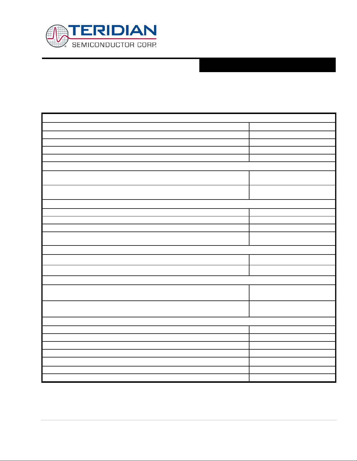
3-Phase Energy Meter IC
DATA SHEET
A Maxim Integrated Products Brand
SPECIFICATIONS
Supplies and Ground Pins:
V3P3D, V3P3A
0.5V to 4.6V
| V3P3D - V3P3A |
0V to 0.5V
VLCD
-0.5V to 7V
VBAT
-0.5V to 4.6V
GNDD
-0.5V to +0.5V
-1mA to 1mA,
-0.5 to V3P3A+0.5V
-1mA to 1mA,
-0.5V to 3.0V
IA, VA, IB, VB, IC, VC, V2, V3
-0.5V to V3P3A+0.5V
XIN, XOUT
-0.5V to 3.0V
RX
-0.5V to 3.6V
-1mA to 1mA
-0.5 to V3P3A+0.5V
Operating junction temperature (peak, 100ms)
140 °C
Operating junction temperature (continuous)
125 °C
Storage temperature
−45 °C to 165 °C
Solder temperature – 10 second duration
250 °C
Pins IA, VA, IB, VB, IC, VC, RX, TX, E_RST, E_TCLK, E_RXTX, E_TBUS[n]
4kV
All other pins
2kV
ABSOLUTE MAXIMUM RATINGS
Analog Output Pins:
VREF, VBIAS
V2P5
Analog Input Pins:
71M6513/71M6513H
AUGUST 2011
Electrical Specifications
−
OPT_RX
Digital Input Pins:
DIO0-21, E_RXTX, E_RST, E_ISYNC/BRKRQ -0.5 to 6V
TEST, RESETZ -0.5 to V3P3D+0.5V
All Oth er Pins:
Input pins
Output pins
Temperature:
ESD Stress:
Stress es b eyond Absolut e Maximum R atings may c ause permanent damage to the device. Thes e are stress ratings only and functional
operati on at thes e or any oth er conditi ons beyond t hose indic ated und er “ recommend ed operat ing conditi ons” is n ot implied. E xposur e to
absolute-maximum-rated conditions for extended periods may affect device reliability. All voltages are with resp ec t to GND A.
-5mA to 5mA
-0.5V to V3P3D+0.5V
-30mA to 30mA
-0.5 to V3P3D+0.5V
Page: 90 of 104 © 2005-2011 Teridian Semiconductor Corporation
Page 91
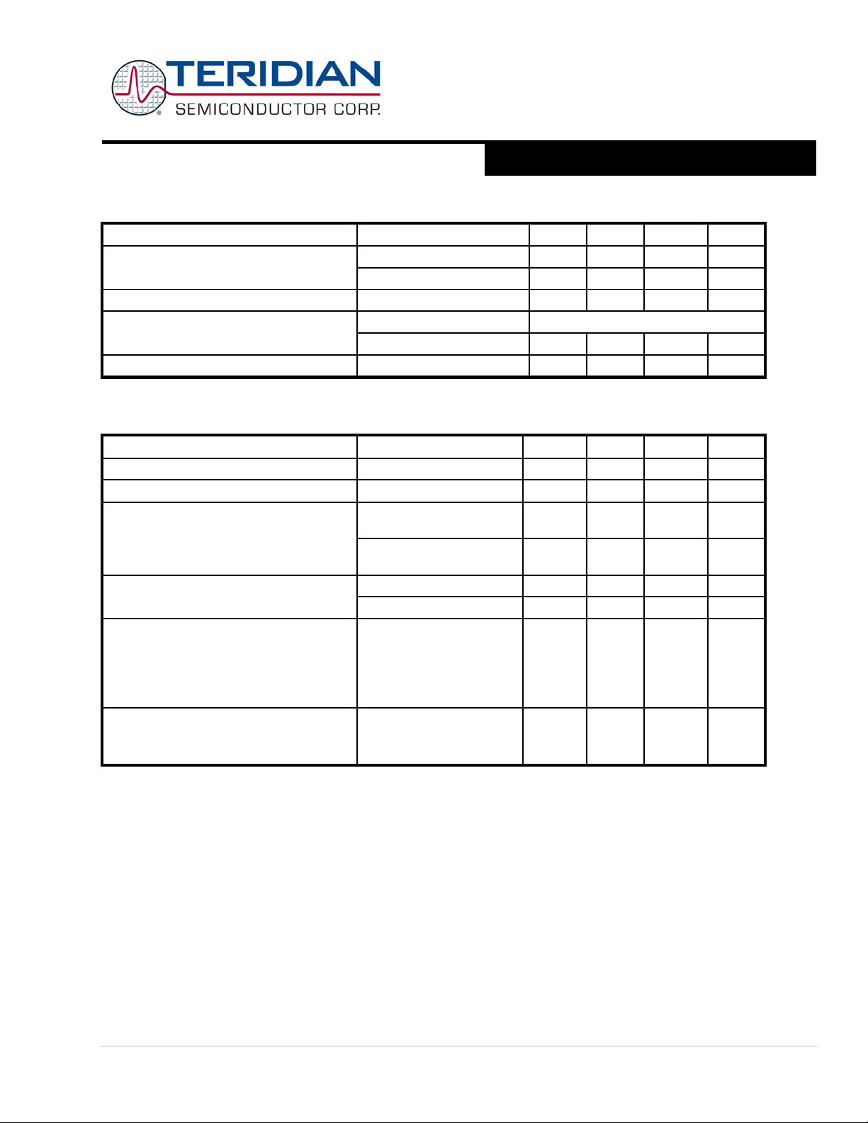
71M6513/71M6513H
3-Phase Energy Meter IC
DATA SHEET
A Maxim Integrated Products Brand
No Battery
Externally Connect to V3P3D
Input pull-up current, IIL
.......
VIN=0V
SEPTEMBER 2011
RECOMMENDED OPERATING CONDITIONS
PARAMETER CONDITION MIN TYP MAX UNIT
3.3V Supply Voltage
(V3P3A, V3P3D)
VLCD 2.9 5.5 V
†
Normal Operation 3.0 3.3 3.6 V
Battery Backup 0 3.45 V
VBAT
Operating Tem perature -40 85 ºC
†
V3P3A and V3P3D should be shorted together on the circuit board. GNDA and GNDD should also be shorted on the circuit board.
Battery Backup 2.0 3.8 V
LOGIC LEVELS
PARAMETER CONDITION MIN TYP MAX UNIT
Digit al high-l evel i nput voltage, VIH 2 V3P3D V
Digit al low-leve l input voltage, VIL
Digit al high-level output voltage VOH
Digit al low-level output volt age VOL
RESETZ
................................
Other digital inputs
Input pull down current, IIH
TEST
Other digital inputs
1
Guaranteed by design; not production tested.
−0.3
= 1mA
I
LOAD
I
= 15mA
LOAD
= 1mA 0 0.4 V
I
LOAD
I
= 15mA 0.81 V
LOAD
VIN=V3P3D
V3P3D
–0.4
V3P3D-
1
0.6
10
10
-1
10
-1
0.8 V
V3P3D V
V
100
100
1
100
1
μA
μA
μA
μA
μA
© 2005-2011 Teridian Semiconductor Corporation Page: 91 of 104
Page 92
71M6513/71M6513H
3-Phase Energy Meter IC
DATA SHEET
A Maxim Integrated Products Brand
VLCD current
0.2
0.4
mA
PARAMETER
CONDITION
MIN
TYP
MAX
UNIT
Reduce V3P3 until V2P5
drops 200mV
PSSR ∆V2P5/∆V3P3
RESETZ=1, iload=0
-3 +3
mV/V
SUPPLY CURRENT
PARAMETER CONDITION MIN TYP MAX UNIT
V3P3A + V3P3D + VLCD current
V3P3A current 3.7 4.3 mA
V3P3D current 2.5 4.8 mA
VBAT current -300 300 nA
V3P3D current
V3P3A + V3P3D current
V3P3D current, Write Flash
VBAT current,
VBAT=3.6V
1
Guaranteed by design; not production tested.
2.5V VOLTAGE REGULATOR
Unless ot herwise spec ified, load = 5mA
Normal Operation,
V3P3A=V3P3D=VLCD=3.3V
CKMPU=614kHz
VBAT=3.6V
No flash memory write
Normal Operation,
V3P3A=V3P3D=VLCD=3.3V
VBAT=3.6V, no flash memory
write
CKMPU=1,228kHz
CKMPU=2,456kHz
CKMPU=4,912kHz
Power save/sleep mode
V3P3A=V3P3D=VLCD=3.3V,
CE, ADC, E_TCLK, VREF disabled
CKMPU=153.5kHz
CKMPU=38.4kHz
Normal Operation as above,
except write Flash at maximum
rate.
Battery backup, ≤25°C
V3P3A=V3P3D=VLCD=0V
f
= 32kHz 85°C
OSC
6.4 9.5 mA
7 mA
2 4 μA
41 121 μA
2.9
3.6
5.1
6
4.9
7
mA
mA
mA
mA
mA
AUGUST 2011
Voltage overhead V3P3-V2P5
Page: 92 of 104 © 2005-2011 Teridian Semiconductor Corporation
440 mV
Page 93
3-Phase Energy Meter IC
DATA SHEET
A Maxim Integrated Products Brand
VREF, VBIAS
PARAMETER
CONDITION
MIN
TYP
MAX
UNIT
VREF output voltage, VNOM(25)
Ta = 22ºC
1.193
1.195
1.197
V
VREF chop step
40
mV
VREF_CAL =1,
ILOAD = 10µA, -10µA
VNOM definitionA
VNOM(T) = VREF(22) + (T–22)TC1 + (T–22)2TC2
V
-- If TRIMBGA and TRIMBGB ava ilable (6513H) --
VREF temperature c oefficients
900
370000_500
2
_
−−
=
BGATRIM
NOMTEMP
y
VREF(T) deviation from VNOM(T)
)40|,22max(|
10)()(
6
−−TVNOM
TVNOMTVREF
-- If TRIMBGA and TRIMBGB not avail able ( 6513) --
VREF temperature c oefficients
TC2 (quad ratic)
-0.341
µV/°C2
VREF(T) deviation from VNOM(T)
)40|,22max(|
10)()(
6
−−TVNOM
TVNOMTVREF
ppm/
year
Ta = 25ºC
Ta = -40ºC to 85ºC
(-1%)
(-2%)1
1.5
1.51
(+1%)
(+2%)1 V V
VBIAS output impedance
ILOAD = 1mA, -1mA
240
500
Ω
PARAMETER
CONDITION
MIN
TYP
MAX
UNIT
Maximum Output Power to Crystal4
Crystal connec ted
1
μW
Xin to Xout Capacitance1
3 pF
Capacitance to DGND1
Xout
5
pF
Watchdog RTC_OK threshold
25
kHz
Unless ot herwise spec ified, VREF_DIS=0
71M6513/71M6513H
SEPTEMBER 2011
VREF output impedance
TC1 (linear)
TC2 (quad ratic)
TRIMBGA, TRIMBGB, TRIMM[ 2:0]: See
x(33-0.28y) + 0.33y + 7.9
x(0.02-0.0002y) – 0.46
where x = 0.1TRIMBGB - 0.14(TRIMM[2:0]+0.5),
2.5 kΩ
TRIMSEL, TRIM registers
-10 10 ppm/ºC
TC1 (linear)
VREF aging Ta = 25ºC ±25
VBIAS output voltage
Ta = -40ºC to +85ºC -40
7.0
1
+401 ppm/ºC
µV/°C
µV/°C
µV/ºC
2
A
This relationship describes the nominal behavior of VREF at different temperatures.
1
Guaranteed by design; not production tested.
CRYSTAL OSCILLATOR
Crystal is disconnected. Test load is series 200pF, 100kΩ connected between DGND and XOUT.
Xin
© 2005-2011 Teridian Semiconductor Corporation Page: 93 of 104
5
pF
Page 94
3-Phase Energy Meter IC
DATA SHEET
A Maxim Integrated Products Brand
ADC CONVERTER, VDD REFERENCED
PARAMETER
CONDITION
MIN
TYP
MAX
UNIT
Recommended Input Range
(Vin-V3P3A)
mV
peak
Voltage to Current Crosstalk:
)cos(
*10
6
VcrosstalkVin
Vin
Vcrosstalk
∠−∠
Vin = 200mV peak, 65Hz,
IC
THD (First 10 harmonics)
20mV- peak
Vin=65Hz,
Harris window
-90
dB
Input Impedance
Vin=65Hz
40 90
kΩ
Temperature c oefficient of Input
Impedance
LSB size
FIR_LEN=0
355
nV/LSB
Digital Full Scal e
+884736
LSB
ADC Gain Error vs
3.3/33100
/35710
6
APV
VnVNout
INPK
∆
∆
Input O ffs et (Vin -V3P3A)
-10 10
mV
PARAMETER
CONDITION
MIN
TYP
MAX
UNIT
OPT_TX VOH (V3P3D-OPT_TX)
ISOURCE=1mA
0.4
V
OPT_TX VOL
ISINK=20mA
0.7
V
OPT_RX Vin Thres hold
(VinRISING+VinFALLING)/2
OPT_RX Vin Hyst eresi s
(VinRISING-VinFALLING)
OPT_RX input i mpedance
|Vin|≤300mV
1
MΩ
PARAMETER
CONDITION
MIN
TYP
MAX
UNIT
Nominal Sensiti v ity (Sn)2
TA=25ºC, TA=75ºC
N(T)= Sn*T+Nn
-900
LSB/ºC
40000
0
Temperature Er ror1
n
S
NTN
TERR
))25()((
)25(
−
−−=
FIR_LEN=0, VREF_DIS=0, VDDREFZ=0
71M6513/71M6513H
AUGUST 2011
-250 250
250mV- peak
%Po wer Supply Variation
1
Guaranteed by design; not production tested.
OPTICAL INTERFACE
on VA, VB, or VC
Vcrosstalk = largest
measurement on IA, IB, or
64kpts FFT, Blackman-
Vin=65Hz 1.7 Ω/°C
Vin=200mV peak, 65Hz
V3P3A=3.0V, 3.6V
200 250 300 mV
-101 101 μV/V
50 ppm/%
-75
dB
TEMPERATURE SENSOR
Nominal Offset (Nn) 2
1
Guaranteed by design; not production tested.
2
This parameter defi nes a nom i nal relationship rather than a meas ured parameter. Correct circu i t operatio n i s veri f ied with
other specs that use thi s nominal relationship as a reference.
Page: 94 of 104 © 2005-2011 Teridian Semiconductor Corporation
5 30 mV
Nominal relationship:
A = -40ºC to +85ºC -3
T
1
31 ºC
LSB
Page 95
3-Phase Energy Meter IC
DATA SHEET
A Maxim Integrated Products Brand
LCD BOOST
PARAMETER
CONDITION
MIN
TYP
MAX
UNIT
VDRV Frequency
OSC/2
Hz
VDRV Sink Current
Vol=1.5V
1.2 2.75
mA
VDRV Source Current
Voh=1.5V
1.2 2.6
mA
VLCD Target Voltage
4.5 5.5
V
VLCD=5.0V,
LCD_BSTEN=1
PARAMETER
CONDITION
MIN
TYP
MAX
UNIT
VLC0 Max Voltage (LCD_FS =1F)
Wi t h respect to VL CD
-0.2 0
V
VLC0 Min Voltage (LCD_FS =00)
Wi t h respect to VL CD*0. 7
-0.2 0.2
V
VLC1 Voltage,
½ bias
Wi t h respect to VL CD/2
-10
+10
%
VLC0 Voltage,
½ bias
Wi t h respect to VLCD/2
-10
+10
%
Output Impedance
∆ILOAD=10µA
30
kΩ
PARAMETER
CONDITION
MIN
TYP
MAX
UNIT
Range for date
2000
-
2255
year
PARAMETER
CONDITION
MIN
TYP
MAX
UNIT
Res et pulse width
5 µs
Res et pulse fall tim e
11
µs
71M6513/71M6513H
SEPTEMBER 2011
VLCD Input Current
LCD_FS=1F,
LCD_MODE=0,1,2,3
450 μA
LCD DRIVERS
App l ies t o all COM and SEG pins. Unless otherw ise st ated, VLCD=5 .0V, LCD_FS=1F
1/3 bias
1/3 bias
Wi t h respect to 2*VLCD/3
Wi t h respect to VL CD/3
-10
-15
RTC
RESETZ
+10
+15
%
%
1
Guaranteed by design; not production tested.
© 2005-2011 Teridian Semiconductor Corporation Page: 95 of 104
Page 96
3-Phase Energy Meter IC
DATA SHEET
A Maxim Integrated Products Brand
COMPARATORS
PARAMETER
CONDITION
MIN
TYP
MAX
UNIT
Offset Voltage
V3-VBIAS
-20
15
mV
Hys teresis Current
V3
0.8
1.2
μA
Response Time
V3
+100mV overdriv e
0.5
50
μs
WD Disabl e Thres hold ( V1-V3P3A)
-400 -10
mV
PARAMETER
CONDITION
MIN
TYP
MAX
UNIT
CKMPU = 4.9MHz
5
Cycles
CKMPU = 1.25MHz
2
Cycles
Flash write cycles
-40°C to +85°C
20,000
Cycles
Flash data reten tion
25°C
100
Years
Flash data reten tion
85°C
10
Years
Flash byte writes between pa ge or mass
erase operations
PARAMETER
CONDITION
MIN
TYP
MAX
UNIT
Write Time per Byte
42
µs
Pag e E rase (512 by tes)
20
ms
Mass Erase
200
ms
PARAMETER
CONDITION
MIN
TYP
MAX
UNIT
CKMPU=4.9MHz, Usin g
interrupts
CKMPU=4.9MHz, “ bitbanging” DIO4/5
71M6513/71M6513H
AUGUST 2011
V1-VBIAS
V2-VBIAS
V1
V2
V1
V2
RAM AND FLASH MEMORY
CE RAM wait states
FLASH MEMORY TIMIN G
Vin = VBIAS - 100mV
2 Cycles
-20
-20
0.8
0.8
2
0.5
15
15
1.2
1.2
15
50
mV
mV
μA
μA
μs
μs
EEPROM INTERFACE
Write Clock frequency
Page: 96 of 104 © 2005-2011 Teridian Semiconductor Corporation
78 kHz
150 kHz
Page 97
71M6513/71M6513H
3-Phase Energy Meter IC
DATA SHEET
A Maxim Integrated Products Brand
Recommended Extern al Co mponents
NAME FROM TO FUNCTION VALUE UNIT
C1 V3P3A AGND Bypass capacitor for 3.3V supply
C2 V3P3D DGND Bypass capacitor for 3.3V supply
XTAL XIN XOUT
CXS XIN AGND
CXL XOUT AGND
CV1 V1 AGND Bypass capacitor for V1
CBIAS VBIAS AGND Bypass capacitor for VBIAS
CBST1 VDRV external Boost charging capacitor
CBST2 VLCD DGND Boost bypass capacitor
C2P5 V2P5 DGND Bypass capacitor for V2P5
RTST TEST DGND Resistor for TEST
32.768kHz crystal. Electrically simila r to ECS
ECX-3TA series
Load capacitor for crystal (depends on crystal
specs and board parasitics).
≥0.1±20% µF
≥0.1±20% µF
32.768 kHz
22±10%
22±10%
≥0.1±20% µF
≥1000±20%
33±20%
≥0.22±20% µF
≥0.1±20% µF
10kΩ±10% µF
SEPTEMBER 2011
pF
pF
pF
nF
© 2005-2011 Teridian Semiconductor Corporation Page: 97 of 104
Page 98
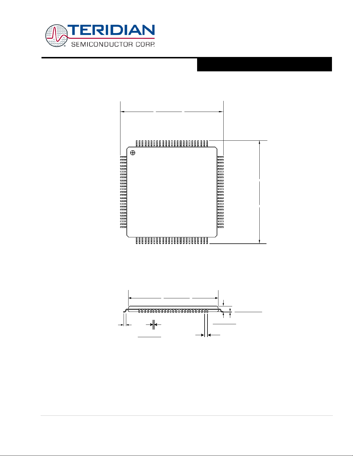
3-Phase Energy Meter IC
DATA SHEET
A Maxim Integrated Products Brand
1
0.50(0.0197)TYP.
0.05(0.002)
0.15(0.006)
0.18(0.007)
0.27(0.011)
0.60(0.024) TYP.
13.8(0.543)
14.2(0.559)
15.7(0.618)
16.3(0.641)
15.7(0.618)
16.3(0.641)
1.40(0.055)
1.60(0.063)
Top View
Side View
Packaging Information
100-Pin LQFP PACKAGE OUTLINE (Bottom View)
71M6513/71M6513H
AUGUST 2011
Notes: Controlling dimensions are in mm.
Page: 98 of 104 © 2005-2011 Teridian Semiconductor Corporation
Page 99
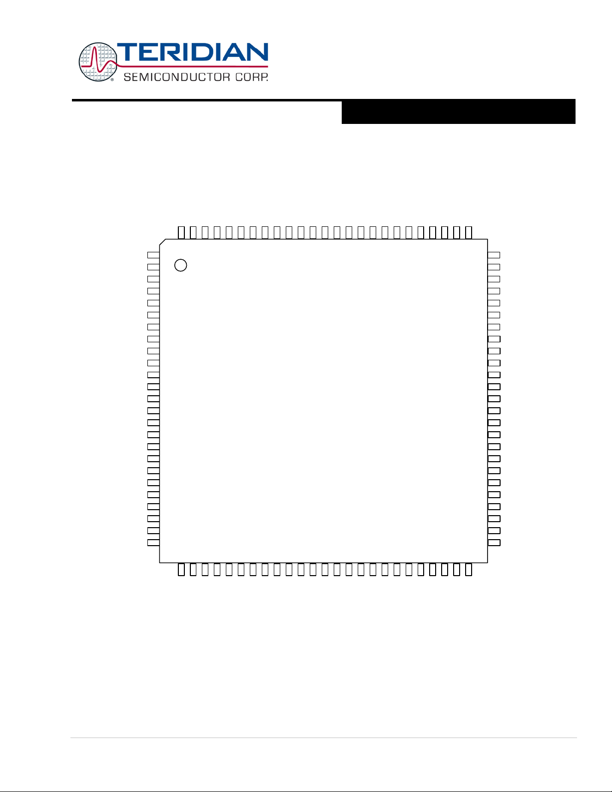
71M6513/71M6513H
3-Phase Energy Meter IC
DATA SHEET
A Maxim Integrated Products Brand
1
2
3
4
5
6
7
8
9
10
11
12
13
14
15
16
17
18
19
20
21
22
23
24
25
2627282930
313233343536373839
4041424344454647484950
63
62
61
60
59
58
57
56
55
54
53
52
51
64
65
66
67
68
69
70
71
72
73
74
75
76
77
78
79
80
81
82
83
84
85
86
87
88
89
90
91
92
93
94
95
96
97
98
99
100
VBIAS
E_TCLK
SEG33/DIO13
SEG32/DIO12
E_RST
VLCDNCXOUT
TEST
XIN
GNDANCOPT_RXV1V2
V3
VREFIAIB
VAVBVC
V3P3A
GNDA
IC
GNDD
SEG14
SEG13
NC
SEG12
SEG11
NC
NC
NC
NC
SEG10
SEG9
SEG7/MUX_SYNC
SEG8
NC
SEG6/SRDY
SEG36/DIO16
NC
SEG35/DIO15
SEG34/DIO14
E_ISYNC/BRKRQ
SEG2
SEG1
SEG15
SEG0
GNDD
E_RXTX
OPT_TX
TMUXOUT
SEG37/DIO17
V3P3D
DIO_3
COM1
COM2
COM3
TX
SEG3/SCLK
VDRV
CKTEST
COM0
SEG4/SSDATA
SEG5/SFR
E_TBUS[3]
E_TBUS[2]
DIO_0
SEG38/DIO18
DIO_1
DIO_2
E_TBUS[0]
E_TBUS[1]
SEG27/DIO7
SEG39/DIO19
SEG26/DIO6
SEG25/DIO5
SEG29/DIO9
RX
SEG31/DIO11
GNDD
RESETZ
V2P5
VBAT
SEG24/DIO4
SEG23
SEG22
SEG28/DIO8
SEG41/DIO21
SEG40/DIO20
NC
SEG19
SEG18
SEG17
SEG16
SEG30/DIO10
SEG20
SEG21
TERIDIAN
71M6513-IGT/71M6513H-IGT
SEPTEMBER 2011
Pinout (Top View)
© 2005-2011 Teridian Semiconductor Corporation Page: 99 of 104
Page 100
71M6513/71M6513H
3-Phase Energy Meter IC
DATA SHEET
A Maxim Integrated Products Brand
Name
Pin #
Type
Description
GNDA
GNDD
V3P3A
V3P3D
Battery backup power supply. A battery or super-capacitor is to be connected between
VBAT and GNDD. If no battery is used, connect VBAT to V3P3D .
32,33,36,
47,55,90,95
Name
Pin #
Type
Circuit
Description
IA
IC
84
82
Line Current Sense Inputs: These pins are voltage inputs to the internal A/D conpins must be connected to V3P3A.
VA
VC
80
78
Line Voltage Sense Inputs: These pins are voltage inputs to the internal A/D conmust be connected to V3P3A.
Comparator Inputs - voltage inputs to the internal comparator: The voltages applied
88.
Reference voltage used by the power fault detection circuit. A 1,000pF capacitor to
GND should be connected to this pin.
Voltage Reference for the ADC. A 0.1µF capacitor to GNDA should be connected to
this pin.
Crystal Inputs: A 32kHz style crystal should be connected across these pins.
manufacturer datasheet for details.
AUGUST 2011
Pin Descriptions
Power/Ground Pins
76,91 P Analog ground: This pin should be connected directly to the analog ground plane.
1, 40, 75 P Digital ground: This pin should be connected directly to the digital ground plane.
77 P Analog power supply: A 3.3V analog power supply should be connected to this pin.
9 P Digital power supply: A 3.3V digital power supply should be connected to this pin.
VBAT 72 P
V2P5 73 O Output of the 2.5V regulato r . A 0.1µF capacitor to GNDA should be connected t o this pin.
VLCD 96 P LCD power supply.
NC
Analog Pins
IB
VB
V1
V2
V3
VBIAS 81 O 9
42,43,44,
83
79
88
87
86
-- No Connect
I 6
I 6
I 7
verter. Typically, they are connected to the output of a current transformer. Unused
verter. Typically, they are con nected t o the output of a resi stor divider. Unused pins
to t hese pins are c ompared to VBIAS . If the volt age is above VBIAS, the corresponding comparator output will be high (1). The outputs are maintained in the
COMP_STAT register. A typical application is to sense the voltage on the DC supply
using an ex ternal resistor divider to scale the power supply voltage to a level that
trigger s the comparator at t he desired vo l tage drop.
V1: This pin is par t of th e reset c i rcui t ry. It also controls the ha rdware watchdog
timer. A 0.1µF capacitor to GNDA should be connected to this pin.
V2: Comparator input. If unused, this pin must be connected to V3P3A or
ground.
V3: Comparator input, also available to the ADC during alternative multiplexer
cycles. If not used for measuring or sensing purposes, the V3 pin should either
be left unconnected or be connected to the VREF pin. See precautions on page
VREF 85 I/O 9
XIN,
XOUT
VDRV 7 O 4 Voltage boost output.
Pin typ es: P = Power, O = Output , I = I npu t, I/O = Input/Output
The circuit number denotes the equivalent circuit, as specified under “I/O Equivalent Circuits”.
Page: 100 of 104 © 2005-2011 Teridian Semiconductor Corporation
92
94
I 8
Typicall y, a 22-27pF cap acit or is also connected from each pin to GNDA. See cry s tal
 Loading...