

Page 1
Rad hard low voltage CMOS 16-bit bus buffer transceiver
(3-state) with 3.6 V tolerant inputs and outputs
Features
■ 1.65 to 3.6 V inputs and outputs
■ High speed A outputs:
–t
= 3.4 ns at V
PD
–t
= 4.3 ns at V
PD
■ Symmetrical impedance A output:
–|I
–|I
■ High speed B outputs:
–t
–t
■ Symmetrical impedance A output:
–|I
–|I
■ Power down protection on inputs and outputs
■ 26 Ω serie resistors in A port output
■ Operating voltage range:
–V
■ Pin and function compatible with 54 series
| = IOL = 12 mA (Min.) at VCC = 3.0 V
OH
| = IOL = 8 mA (Min.) at VCC = 2.3 V
OH
= 2.5 ns (Max.) at V
PD
= 3.2 ns (Max.) at V
PD
| = IOL = 24 mA (Min.) at VCC = 3.0 V
OH
| = IOL = 18 mA (Min.) at VCC = 2.3 V
OH
(Opr) = 1.65 V to 3.6 V
CC
H162245
■ Bus hold provided on both sides
■ Cold spare function
■ Latch-up performance exceeds
300 mA (JESD 17)
■ ESD performance:
– HBM > 2000 V
(MIL STD 883 method 3015); MM > 200 V
■ 300 krad Mil1019.6 condition A, (RHA QML
qualification extension undergone)
■ No SEL, no SEU and no SET under 110
Mev/cm2/mg LET heavy ions irradiation
■ QML qualified product
■ Device fully compliant with
DSCC SMD 5962-02508
■ 100 mV typical Input hysteresis
= 3.0 to 3.6 V
CC
= 2.3 to 2.7 V
CC
CC
CC
= 3.0 to 3.6 V
= 2.3 to 2.7 V
54VCXH162245
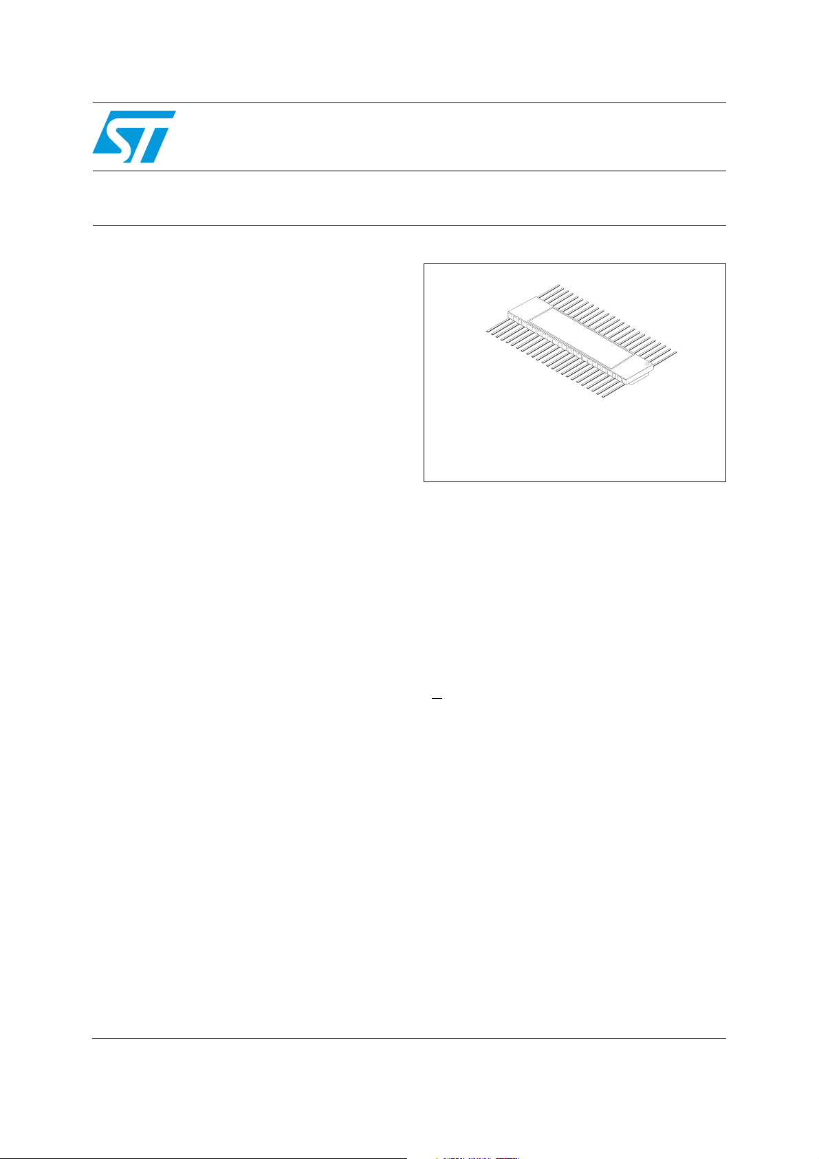
Flat-48
The upper metallic lid is not electrically connected to any
pins, nor to the IC die inside the package.
Description
The 54VCXH162245 is a low voltage CMOS 16
bit bus transceiver (3-state) fabricated with submicron silicon gate and five-layer metal wiring
C²MOS technology. It is ideal for low power and
very high speed 1.65 to 3.6 V applications; it can
be interfaced to 3.6 V signal environment for both
inputs and outputs. This IC is intended for twoway asynchronous communication between data
buses; the direction of data transmission is
determined by DIR input. The two enable inputs
nG
can be used to disable the device so that the
buses are effectively isolated. The device circuits
is including 26 Ω series resistance in the A port
outputs. These resistors permit to reduce line
noise in high speed applications. Bus hold on
data inputs is provided in order to eliminate the
need for external pull-up or pull-down resistor. All
inputs and outputs are equipped with protection
circuits against static discharge, giving them 2 kV
ESD immunity and transient excess voltage. All
floating bus terminals during high Z state must be
held HIGH or LOW.
July 2011 Doc ID 10632 Rev 9 1/19
www.st.com
19
Page 2

Contents 54VCXH162245
Contents
1 Logic symbols and I/O equivalent circuit . . . . . . . . . . . . . . . . . . . . . . . . 3
2 Pin settings . . . . . . . . . . . . . . . . . . . . . . . . . . . . . . . . . . . . . . . . . . . . . . . . 4
2.1 Pin connection . . . . . . . . . . . . . . . . . . . . . . . . . . . . . . . . . . . . . . . . . . . . . . 4
2.2 Pin description . . . . . . . . . . . . . . . . . . . . . . . . . . . . . . . . . . . . . . . . . . . . . . 5
2.3 Truth table . . . . . . . . . . . . . . . . . . . . . . . . . . . . . . . . . . . . . . . . . . . . . . . . . . 5
3 Maximum rating . . . . . . . . . . . . . . . . . . . . . . . . . . . . . . . . . . . . . . . . . . . . . 6
3.1 Recommended operating conditions . . . . . . . . . . . . . . . . . . . . . . . . . . . . . 7
4 Electrical characteristics . . . . . . . . . . . . . . . . . . . . . . . . . . . . . . . . . . . . . 8
5 Test circuit . . . . . . . . . . . . . . . . . . . . . . . . . . . . . . . . . . . . . . . . . . . . . . . . 12
6 Waveforms . . . . . . . . . . . . . . . . . . . . . . . . . . . . . . . . . . . . . . . . . . . . . . . . 13
7 Package mechanical data . . . . . . . . . . . . . . . . . . . . . . . . . . . . . . . . . . . . 15
8 Order codes . . . . . . . . . . . . . . . . . . . . . . . . . . . . . . . . . . . . . . . . . . . . . . . 17
9 Revision history . . . . . . . . . . . . . . . . . . . . . . . . . . . . . . . . . . . . . . . . . . . 18
2/19 Doc ID 10632 Rev 9
Page 3
54VCXH162245 Logic symbols and I/O equivalent circuit
1 Logic symbols and I/O equivalent circuit
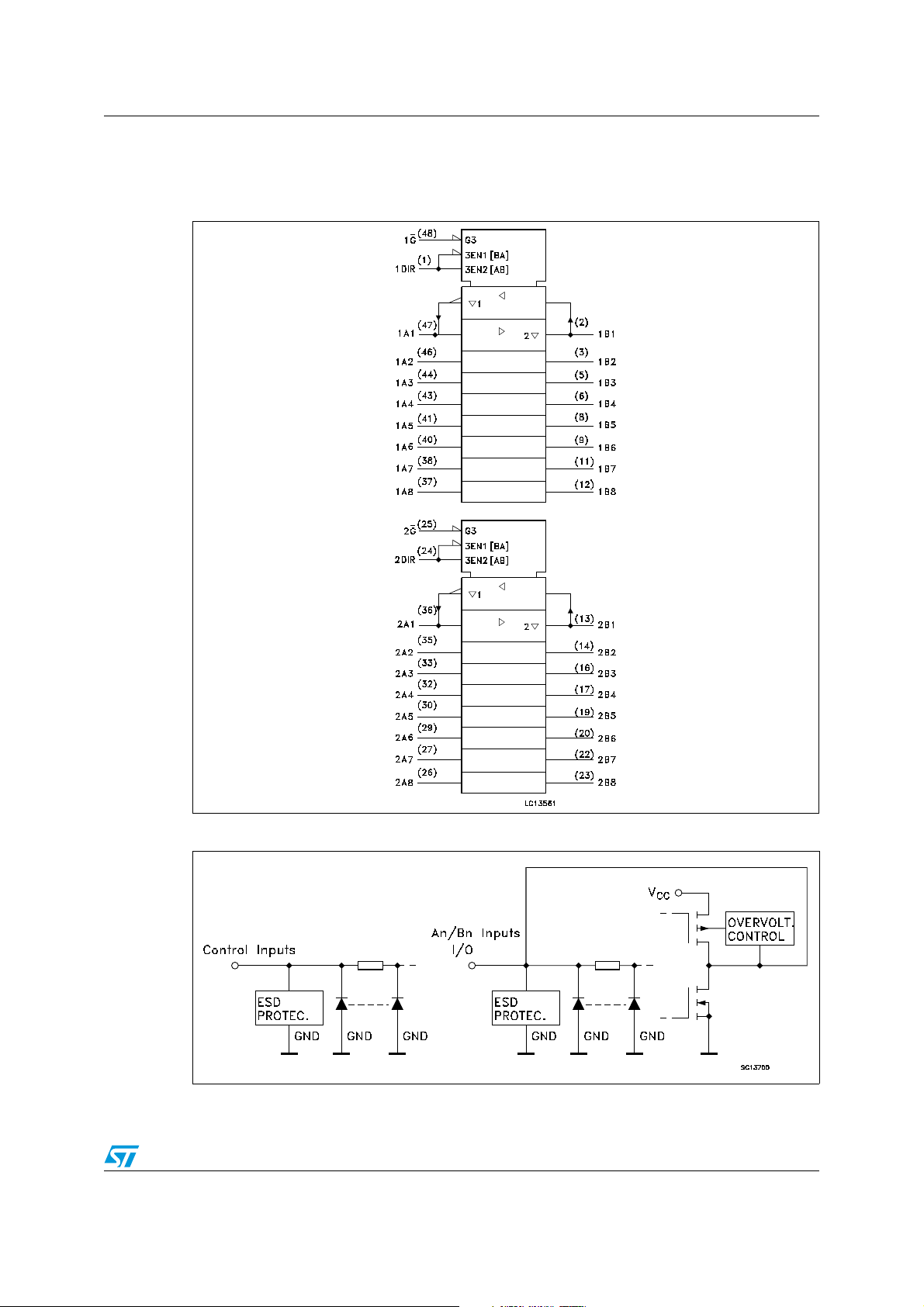
Figure 1. IEC logic symbols
Figure 2. Input and output equivalent circuit
Doc ID 10632 Rev 9 3/19
Page 4
Pin settings 54VCXH162245
2 Pin settings
2.1 Pin connection
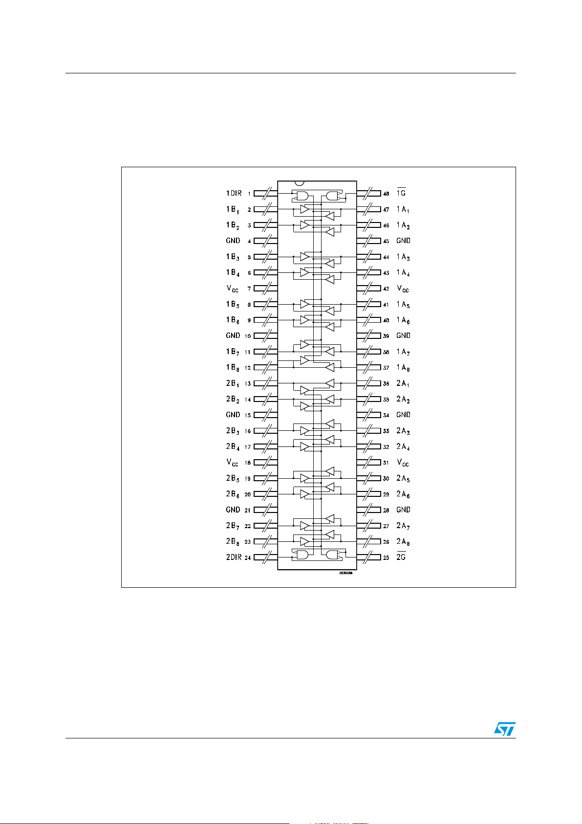
Figure 3. Pin connection (top through view)
4/19 Doc ID 10632 Rev 9
Page 5
54VCXH162245 Pin settings
2.2 Pin description
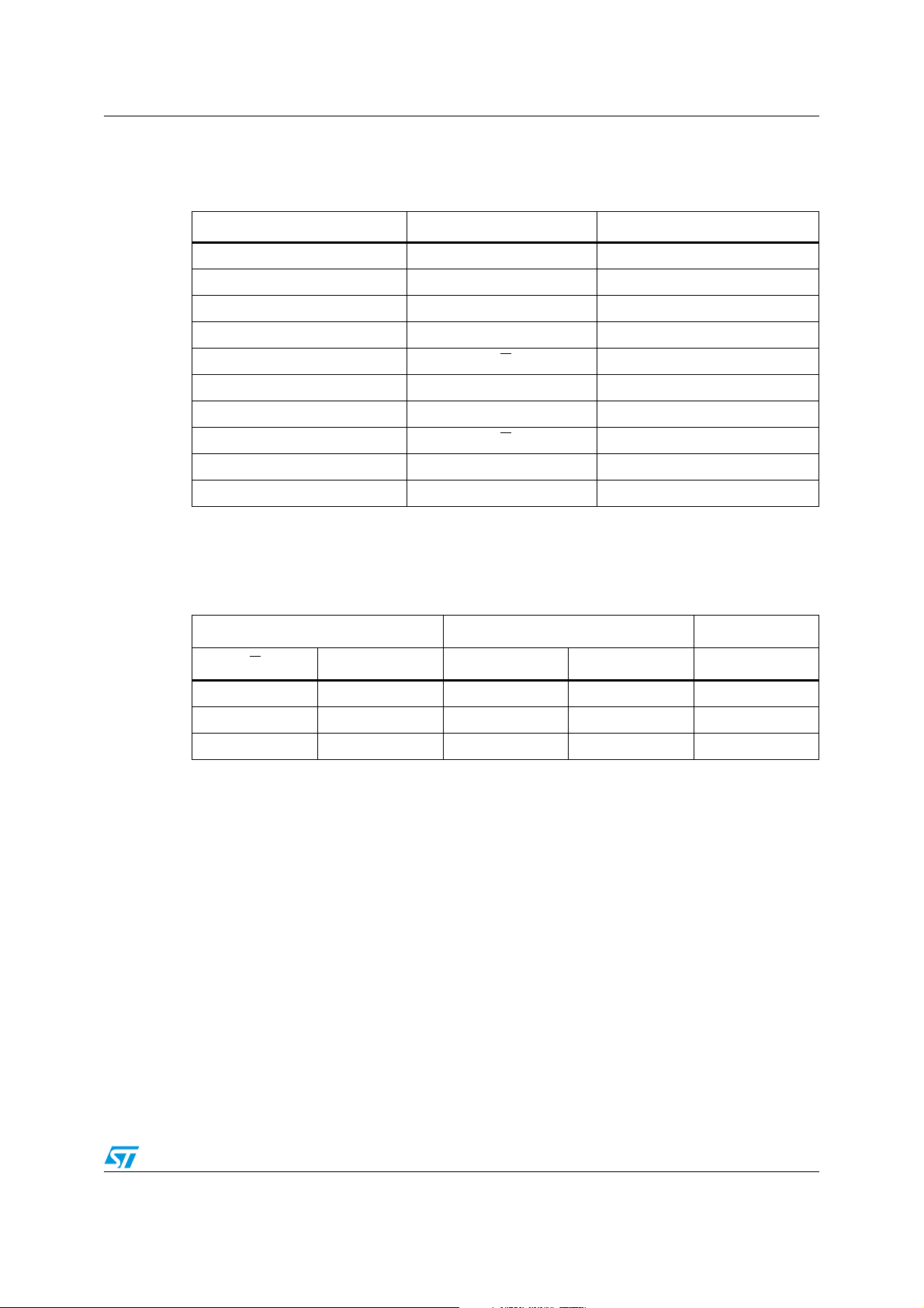
Table 1. Pin description
Pin n° Symbol Name and function
1 1DIR Directional control
2, 3, 5, 6, 8, 9, 11, 12 1B1 to 1B8 Data inputs/outputs
13, 14, 16, 17, 19, 20, 22, 23 2B1 to 2B8 Data inputs/outputs
24 2DIR Directional control
25 2G
36, 35, 33, 32, 30, 29, 27, 26 2A1 to 2A8 Data inputs/outputs
47, 46, 44, 43, 41, 40, 38, 38 1A1 to 1A8 Data inputs/outputs
Output enable input
48 1G
4, 10, 15, 21, 28, 34, 39, 45 GND Ground (0 V)
7, 18, 31, 42 V
2.3 Truth table
Table 2. Truth table
Inputs Function Output
G
L L output input A = B
L H input output B = A
HXZ Z Z
Note: X = Do not care; Z = High Impedance
DIR A bus B bus Yn
CC
Output enable input
Positive supply voltage
Doc ID 10632 Rev 9 5/19
Page 6
Maximum rating 54VCXH162245
3 Maximum rating
Stressing the device above the rating listed in the “absolute maximum ratings” table may
cause permanent damage to the device. These are stress ratings only and operation of the
device at these or any other conditions above those indicated in the operating sections of
this specification is not implied. Exposure to absolute maximum rating conditions for
extended periods may affect device reliability.
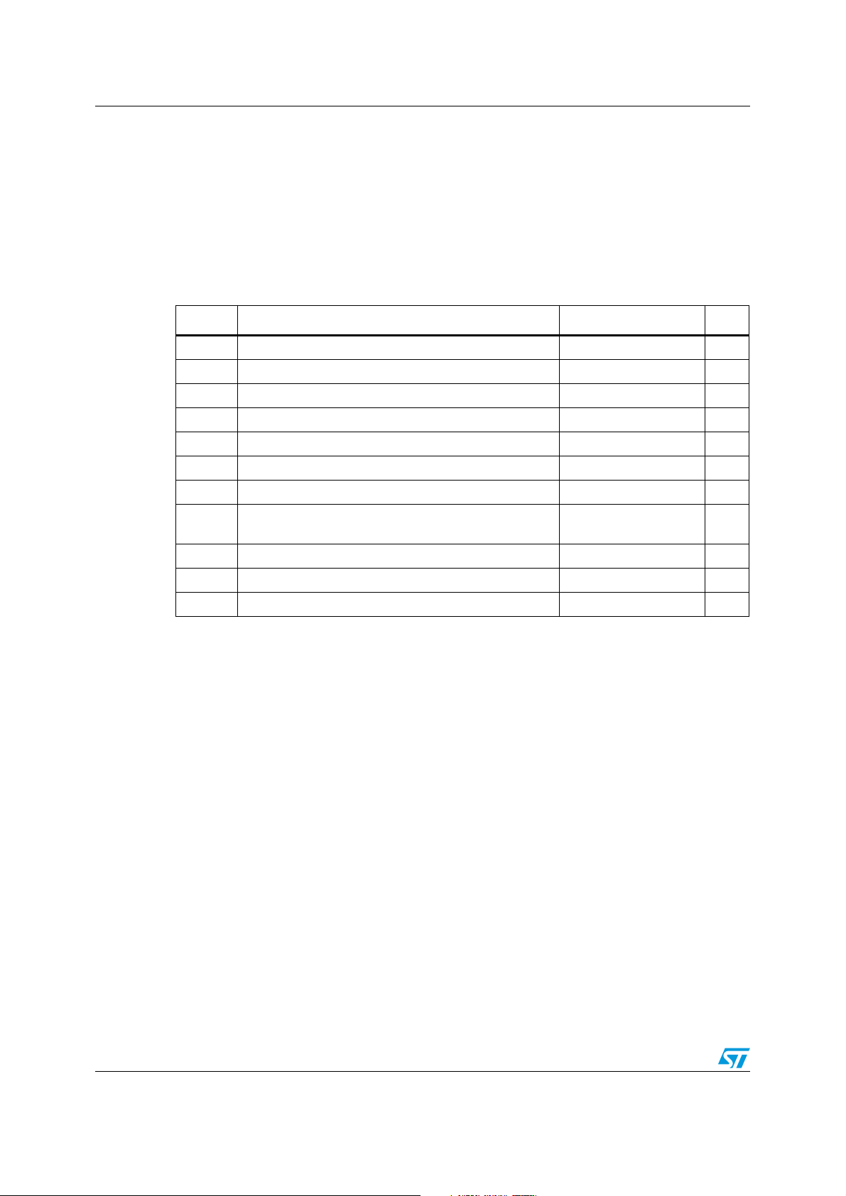
Table 3. Absolute maximum ratings
Symbol Parameter Value Unit
I
CC
I
V
I
GND
T
Supply voltage -0.5 to +4.6 V
CC
DC input voltage -0.5 to +4.6 V
V
I
V
DC output voltage (OFF state) -0.5 to +4.6 V
O
DC output voltage (high or low state)
V
O
I
DC input diode current - 50 mA
IK
DC output diode current
OK
DC output current ± 50 mA
I
O
or
DC VCC or ground current per supply pin ± 100 mA
P
Power dissipation 400 mW
D
Storage temperature -65 to +150 °C
stg
Lead temperature (10 sec) 260 °C
T
L
(2)
1. IO absolute maximum rating must be observed
2. VO < GND, VO > V
CC
(1)
-0.5 to VCC + 0.5 V
- 50 mA
6/19 Doc ID 10632 Rev 9
Page 7
54VCXH162245 Maximum rating
3.1 Recommended operating conditions
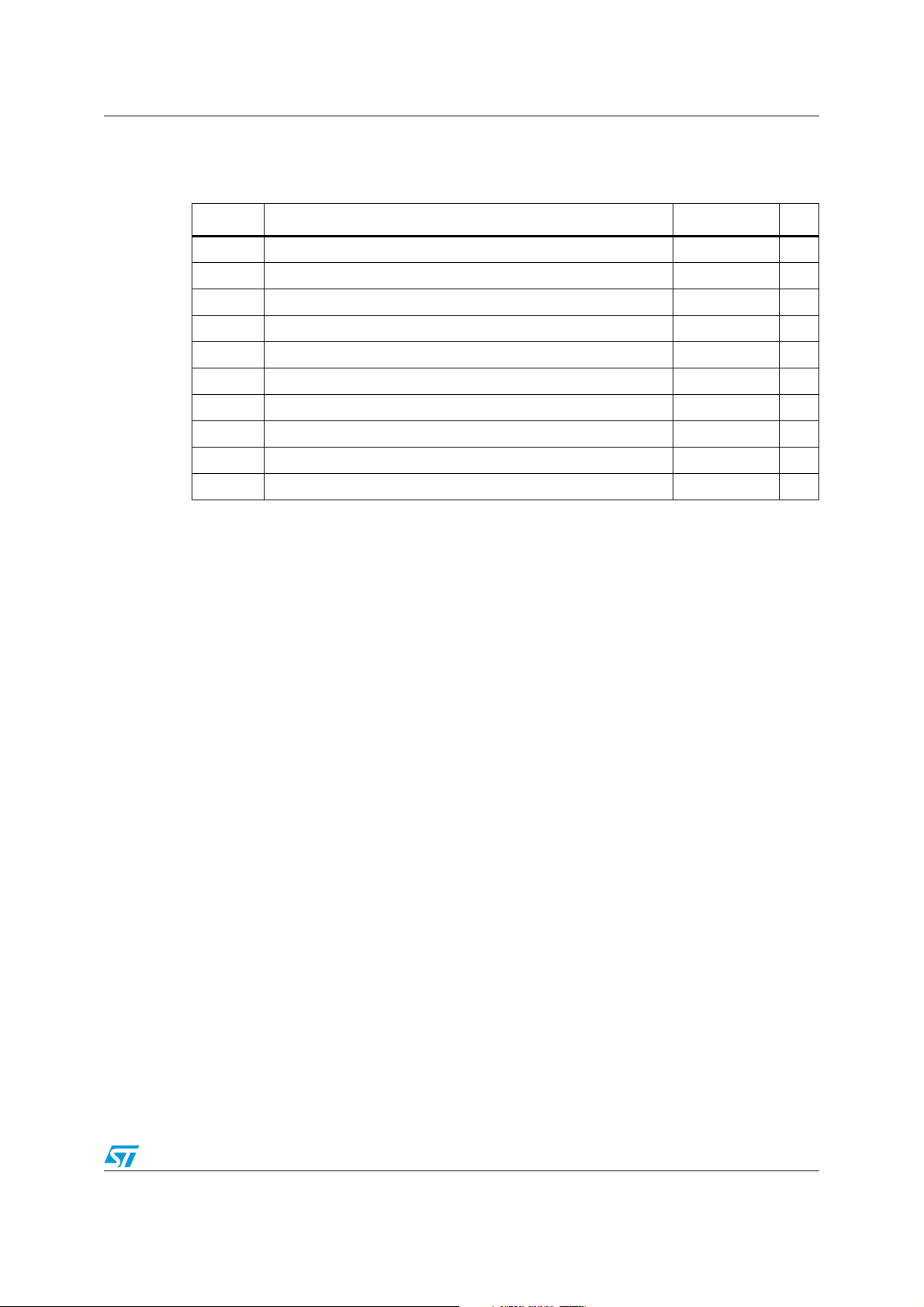
Table 4. Recommended operating conditions
Symbol Parameter Value Unit
I
I
I
I
V
V
V
OH
OH
OH
OH
T
Supply voltage 1.8 to 3.6 V
CC
Input voltage -0.3 to 3.6 V
V
I
Output voltage (OFF state) 0 to 3.6 V
O
Output voltage (high or low state) 0 to V
O
, I
High or low level output current - A side (VCC = 3.0 to 3.6 V) ± 12 mA
OL
, I
High or low level output current - A side (VCC = 2.3 to 2.7 V) ± 8mA
OL
, I
High or low level output current - B side (VCC = 3.0 to 3.6 V) ± 24 mA
OL
, I
High or low level output current - B side (VCC = 2.3 to 2.7 V) ± 18 mA
OL
Operating temperature -55 to 125 °C
op
dt/dv Input rise and fall time
1. VIN from 0.8 V to 2 V at VCC = 3.0 V
(1)
CC
V
0 to 10 ns/V
Doc ID 10632 Rev 9 7/19
Page 8
Electrical characteristics 54VCXH162245
4 Electrical characteristics
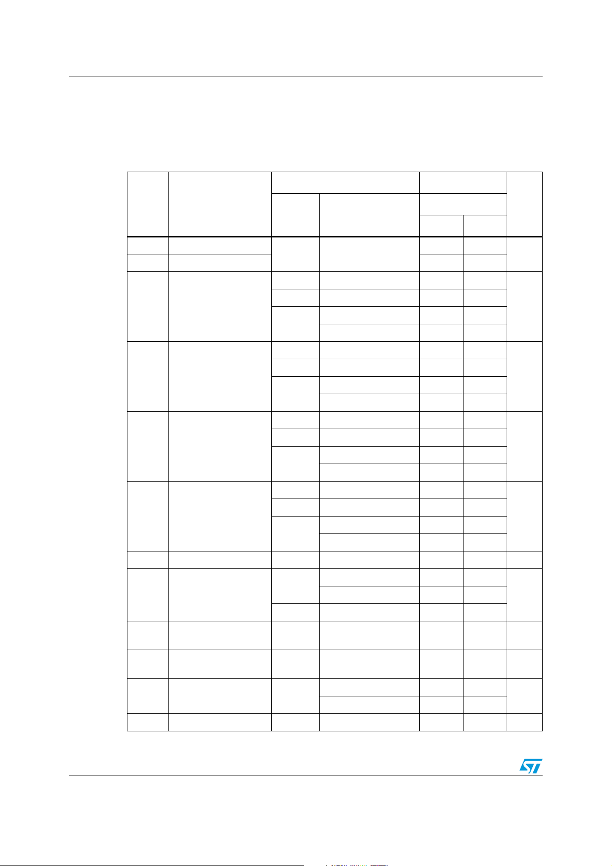
2.7 V < VCC < 3.6 V unless otherwise specified.
Table 5. DC specifications
Test condition Value
Symbol Parameter
V
CC
(V)
V
High level input voltage
IH
Low level input voltage 0.8
V
IL
High level output
V
OH
voltage
(A outputs)
High level output
V
OH
voltage
(B outputs)
Low level output
V
OL
voltage
(A outputs)
Low level output
OL
voltage
V
(B outputs)
Input leakage current 2.7 to 3.6 VI = 0 to 3.6 V ± 5 μA
I
I
I
I(HOLD)
ΔI
Input hold current
Power off leakage
I
off
current
High impedance output
I
OZ
leakage current
Quiescent supply
I
CC
current
CCICC
incr. per input 2.7 to 3.6 VIH = VCC - 0.6 V 750 μA
2.7 to 3.6
2.7 to 3.6 I
2.7 I
3.0
2.7 to 3.6 I
2.7 I
3.0
2.7 to 3.6 I
2.7 I
3.0
2.7 to 3.6 I
2.7 I
3.0
3.0
3.6 V
0V
2.7 to 3.6
2.7 to 3.6
or VO = 0 to 3.6 V 10 μA
I
V
VO = 0 to 3.6 V
V
I
or VO = VCC to 3.6 V ± 20
V
I
=-100 μAV
O
=-6 mA 2.2
O
I
=-8 mA 2.4
O
I
=-12 mA 2.2
O
=-100 μAV
O
=-12 mA 2.2
O
I
=-18 mA 2.4
O
=-24 mA 2.2
I
O
=100 μA0.2
O
=6 mA 0.4
O
I
=8 mA 0.55
O
I
=12 mA 0.8
O
=100 μA0.2
O
=12 mA 0.4
O
I
=18 mA 0.4
O
=24 mA 0.55
I
O
V
= 0.8 V 75
I
= 2 V -75
I
= 0 to 3.6 V ± 500
I
= VIH or V
I
IL
= VCC or GND 20
-55 to 125 °C
Min. Max.
2.0
-0.2
CC
-0.2
CC
± 10 μA
Unit
V
V
V
V
V
μAV
μA
8/19 Doc ID 10632 Rev 9
Page 9
54VCXH162245 Electrical characteristics
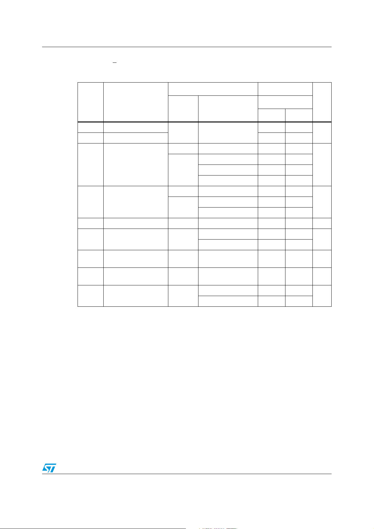
2.3 V < VCC < 2.7 V unless otherwise specified.
Table 6. DC specifications
Test condition Value
Symbol Parameter
V
High level input voltage
IH
Low level input voltage 0.7
V
IL
V
V
I
I(HOLD)
High level output voltage
OH
Low level output voltage
OL
Input leakage current 2.3 to 2.7 VI = VCC or GND ± 5 μA
I
I
Input hold current 2.3
Power off leakage
I
off
current
High impedance output
I
OZ
leakage current
V
CC
(V)
2.3 to 2.7
2.3 to 2.7 I
2.3
2.3 to 2.7 I
2.3
0V
2.3 to 2.7
or VO = 0 to 3.6 V 10 μA
I
VI = VIH or V
VO = 0 to 3.6 V
-55 to 125 °C
Unit
Min. Max.
1.6
V
=-100 μAVCC-0.2
O
I
=-4 mA 2.0
O
=-6 mA 1.8
I
O
I
=-8 mA 1.7
O
=100 μA0.2
O
I
=6 mA 0.4
O
=8 mA 0.6
I
O
V
V
VI = 0.7 V 45
μA
= 1.7 V -45
V
I
IL
± 10 μA
= VCC or GND 20
V
Quiescent supply
I
CC
current
2.3 to 2.7
I
or VO = VCC to 3.6V ± 20
V
I
μA
Doc ID 10632 Rev 9 9/19
Page 10
Electrical characteristics 54VCXH162245
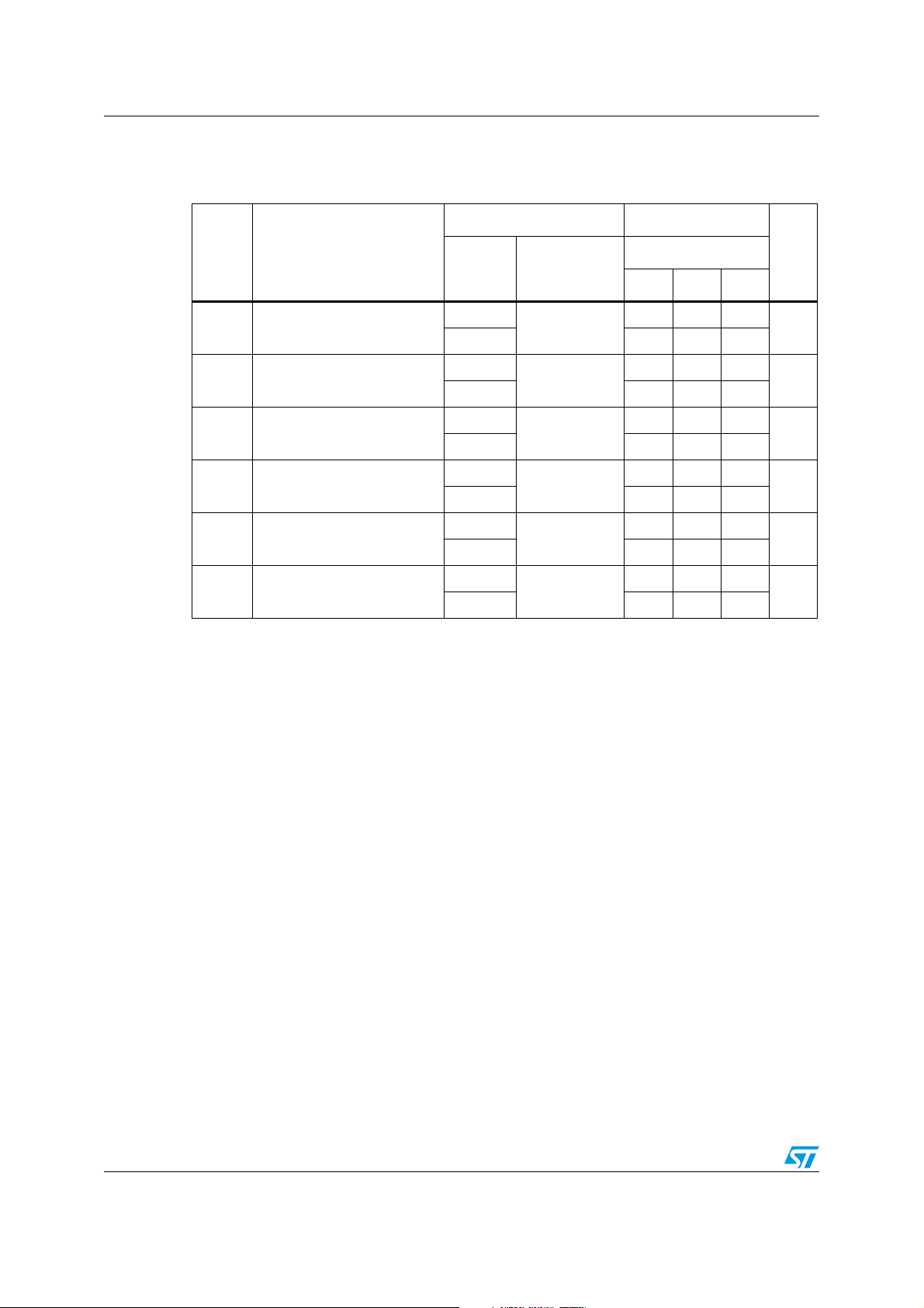
TA = 25 °C, Input tr = tf = 2.0 ns, CL = 30 pF, RL = 500 Ω
Table 7. Dynamic switching characteristics
Test condition Value
Symbol Parameter
V
CC
(V)
V
V
V
V
V
V
1. Number of outputs defined as “n”. Measured with “n-1” outputs switching from HIGH to LOW or LOW to
2. Parameters guaranteed by design.
3. Number of outputs defined as “n”. Measured with “n-1” outputs switching from HIGH to LOW or LOW to
Dynamic peak low voltage
OLP
quiet output
Dynamic peak low voltage
OLP
quiet output
Dynamic valley low voltage
OLV
quiet output
Dynamic valley low voltage
OLV
quiet output
Dynamic valley high voltage
OHV
quiet output
Dynamic valley high voltage
OHV
quiet output
HIGH. The remaining output is measured in the LOW state.
HIGH. The remaining output is measured in the HIGH state.
(1) (2)
(1) (2)
(1) (2)
(1) (2)
(2) (3)
(2) (3)
(A to B)
(B to A)
(A to B)
(B to A)
(A to B)
(B to A)
2.5
3.3 - 0.8 -
2.5
3.3 - 0.35 -
2.5
3.3 - -0.8 -
2.5
3.3 - -0.35 -
2.5
3.3 - 2.2 -
2.5
3.3 - 2.65 -
V
= 0V
IL
VIH = V
VIL = 0V
VIH = V
V
= 0V
IL
= V
V
IH
V
= 0V
IL
= V
V
IH
V
= 0V
IL
VIH = V
VIL = 0V
VIH = V
CC
CC
CC
CC
CC
CC
TA = 25 °C
Min. Typ. Max.
-0.6-
-0.25-
--0.6-
- -0.25 -
-1.9-
-2.05-
Unit
V
V
V
V
V
V
10/19 Doc ID 10632 Rev 9
Page 11
54VCXH162245 Electrical characteristics
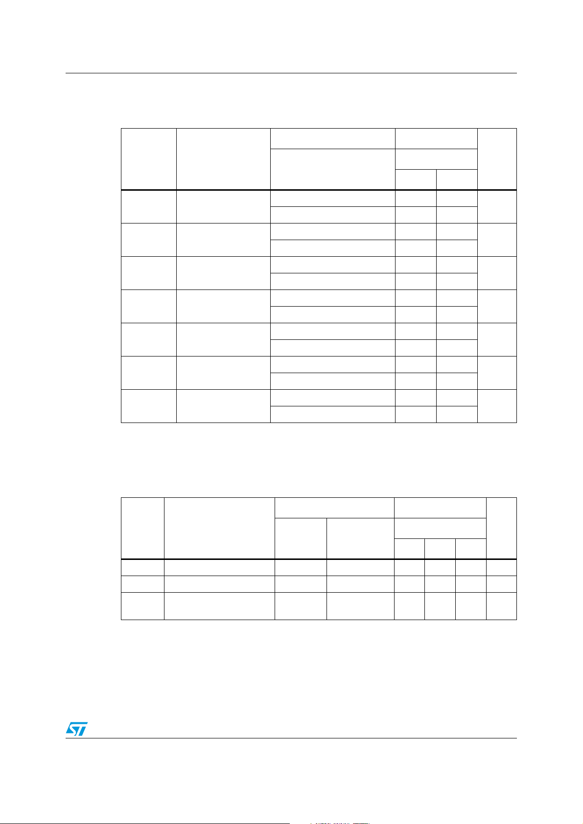
CL = 30 pF, RL = 500 Ω, Input tr = tf = 2.0 ns
Table 8. AC electrical characteristics
Test condition Value
Symbol Parameter
V
CC
(V)
t
PLH tPHL
t
PLH tPHL
t
PZL tPZH
t
PZL tPZH
t
PLZ tPHZ
t
PLZ tPHZ
t
OSLH tOSHL
1. Skew is defined as the absolute value of the difference between the actual propagation delay for any two
outputs of the same device switching in the same direction, either HIGH or LOW (t
t
OSHL
2. Parameter guaranteed by design
Propagation delay
time (A to B)
Propagation delay
time (B to A)
Output enable time
(A to B)
Output enable time
(B to A)
Output disable time
(A to B)
Output disable time (B
to A)
Output to output skew
(1) (2)
time
= | t
PHLm
- t
PHLn
|)
2.3 to 2.7 1.0 4.0
3.0 to 3.6 0.8 3.6
2.3 to 2.7 1.0 4.9
3.0 to 3.6 0.8 4.0
2.3 to 2.7 1.0 5.8
3.0 to 3.6 0.8 4.3
2.3 to 2.7 1.0 6.8
3.0 to 3.6 0.8 4.8
2.3 to 2.7 1.0 4.8
3.0 to 3.6 0.8 5.6
2.3 to 2.7 1.0 5.7
3.0 to 3.6 0.8 7.0
2.3 to 2.7 0.5
3.0 to 3.6 0.5
-55 to 125 °C
Min. Max.
= | t
OSLH
PLHm
- t
Unit
PLHn
ns
ns
ns
ns
ns
ns
ns
|,
Table 9. Capacitive characteristics
Test condition Value
Symbol Parameter
V
CC
(V)
C
C
C
1. CPD is defined as the value of the IC’s internal equivalent capacitance which is calculated from the
operating current consumption without load. (Refer to test circuit). Average operating current can be
obtained by the following equation. I
Input capacitance 2.5 or 3.3 VIN = 0 or V
IN
Output capacitance 2.5 or 3.3 VIN = 0 or V
OUT
Power dissipation
PD
capacitance
(1)
2.5 or 3.3
= CPD x VCC x fIN + ICC/16 (per circuit)
CC(opr)
= 10 MHz
f
IN
VIN = 0 or V
CC
CC
CC
= 25 °C
T
A
Min. Typ. Max.
-4-pF
-8-pF
-28-pF
Doc ID 10632 Rev 9 11/19
Unit
Page 12
Test circuit 54VCXH162245
5 Test circuit
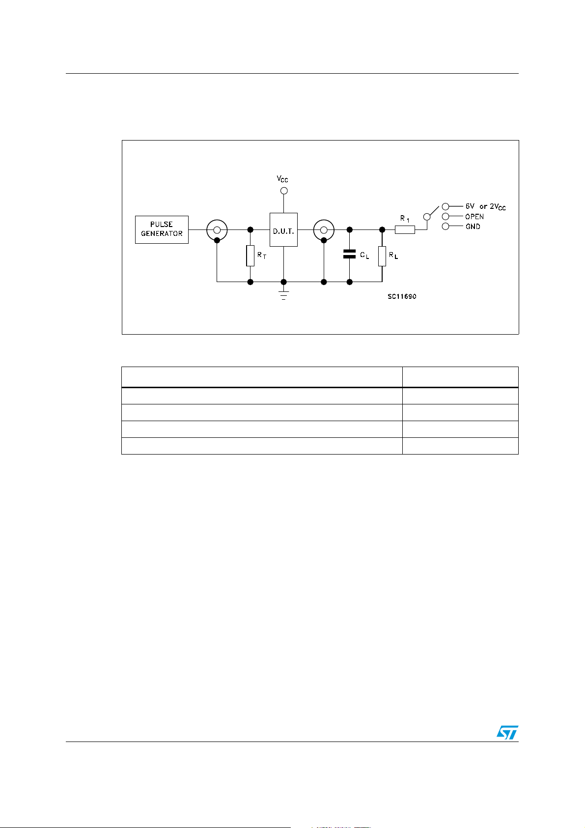
Figure 4. Test circuit
Table 10. Test circuit
Tes t Sw itch
t
, t
PLH
PHL
, t
t
PZL
PLZ (VCC
, t
t
PZL
PLZ (VCC
t
, t
PZH
PHZ
C
= 30 pF or equivalent (includes jig and probe capacitance)
L
R
= R1 = 500 Ω or equivalent
L
R
= Z
T
OUT
= 3.0 to 3.6 V) 6V
= 2.3 to 2.7 V) 2V
of pulse generator (typically 50 Ω)
Open
CC
GND
12/19 Doc ID 10632 Rev 9
Page 13
54VCXH162245 Waveforms
6 Waveforms
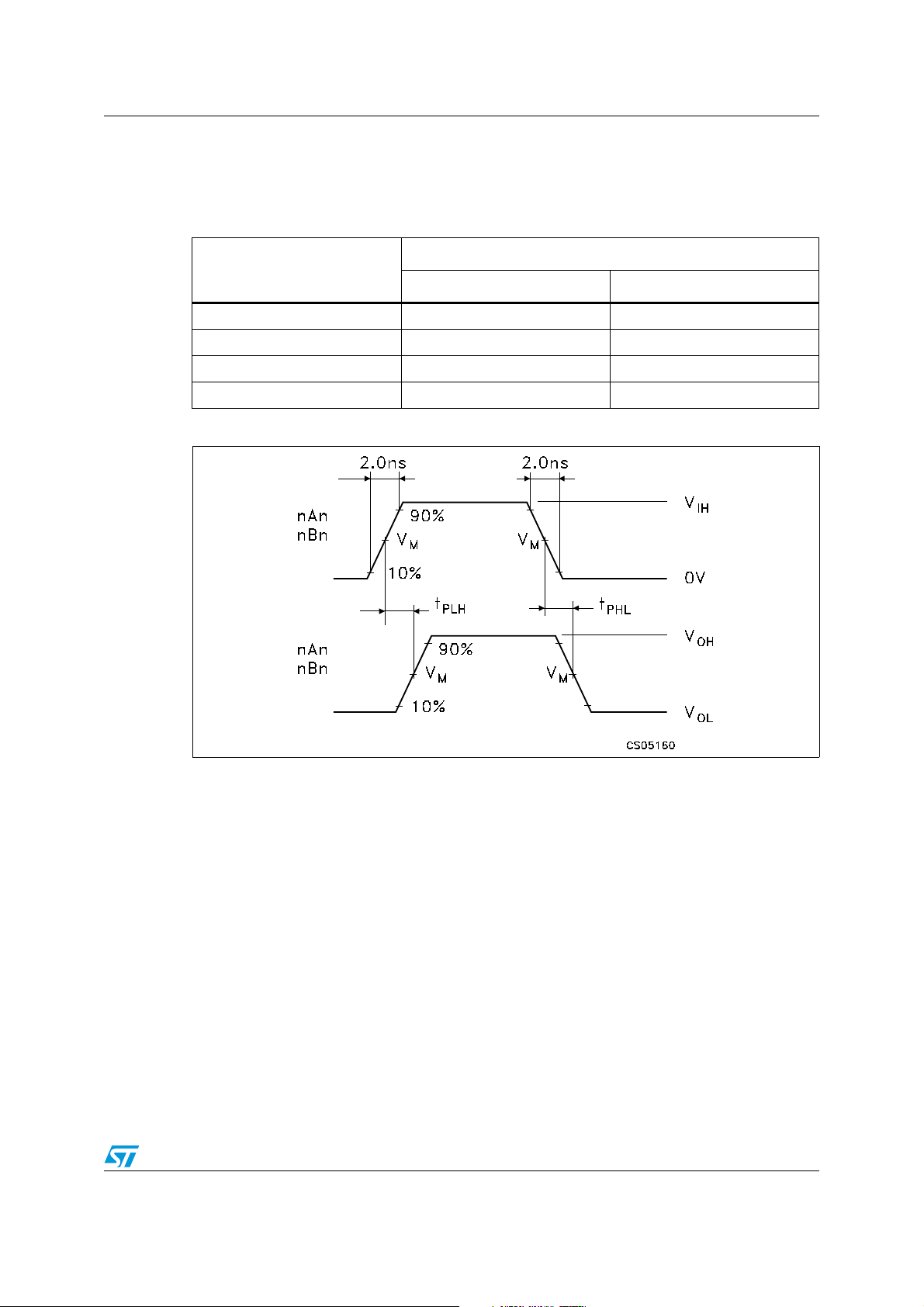
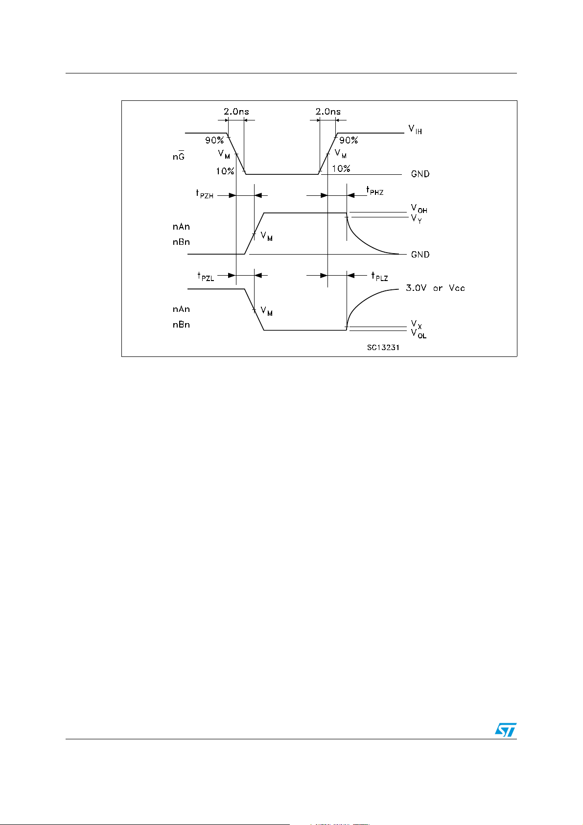
Table 11. Waveform symbol value
V
Symbol
3.0 to 3.6 V 2.3 to 2.7 V
CC
V
IH
V
M
V
X
V
Y
2.7V V
1.5V VCC/2
VOL +0.3V VOL +0.15V
VOH -0.3V VOH -0.15V
Figure 5. Waveform - propagation delay (f = 1 MHz; 50% duty cycle)
CC
Doc ID 10632 Rev 9 13/19
Page 14
Waveforms 54VCXH162245
Figure 6. Waveform - output enable and disable time (f = 1 MHz; 50% duty cycle)
14/19 Doc ID 10632 Rev 9
Page 15
54VCXH162245 Package mechanical data
7 Package mechanical data
54VCXH162245 Products are supplied into ceramic body / metal lid hermetic Flat 48-pin
space package
In order to meet environmental requirements, ST offers these devices in different grades of
ECOPACK
specifications, grade definitions and product status are available at: www.st.com.
ECOPACK
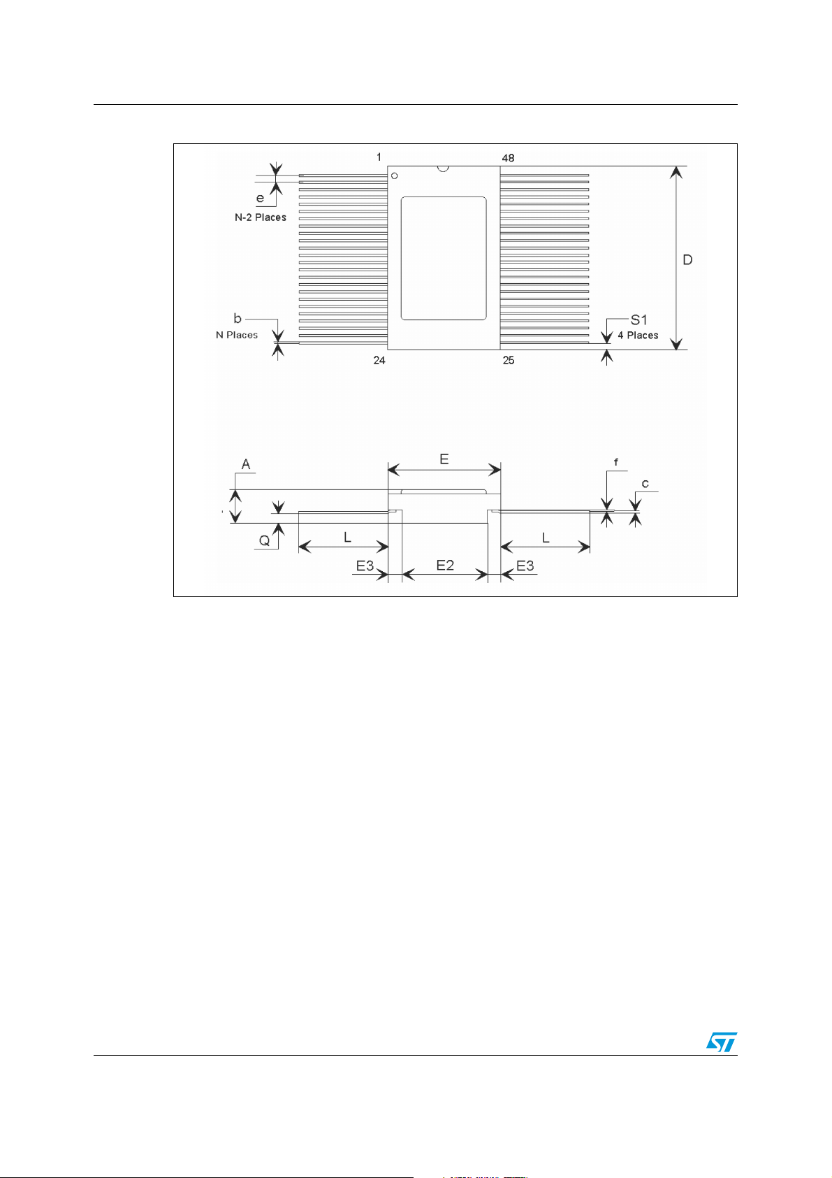
Table 12. Flat-48 (MIL-STD-1835) mechanical data
®
packages, depending on their level of environmental compliance. ECOPACK®
®
is an ST trademark.
mm inch
Dim.
Min. Typ. Max. Min. Typ. Max.
A 2.18 2.47 2.72 0.086 0.097 0.107
b 0.20 0.254 0.30 0.008 0.010 0.012
c 0.12 0.15 0.18 0.005 0.006 0.007
D 15.57 15.75 15.92 0.613 0.620 0.627
E 9.52 9.65 9.78 0.375 0.380 0.385
E2 6.22 6.35 6.48 0.245 0.250 0.255
E3 1.52 1.65 1.78 0.060 0.065 0.070
e 0.635 0.025
f 0.20 0.008
L 6.85 8.38 9.40 0.270 0.330 0.370
Q 0.66 0.79 0.92 0.026 0.031 0.036
S1 0.25 0.43 0.61 0.010 0.017 0.024
Doc ID 10632 Rev 9 15/19
Page 16
Package mechanical data 54VCXH162245
Figure 7. Package dimension
Note: The upper metallic lid is not electrically connected to any pins, nor to the IC die inside the
package. Connecting unused pins or metal lid to ground or to the power supply will not affect
the electrical characteristics.
7330585B
16/19 Doc ID 10632 Rev 9
Page 17

54VCXH162245 Order codes
8 Order codes
Table 13. Ordering information
Package
Min op.
voltage
48-pin flat 1.8 V
Lead
finish
gold
plated
Radiation
level
Flight models
Engineering model Packing
QML-V
300 krad RHFXH162245K03V RHRXH162245K1 Conductive strip pack
Doc ID 10632 Rev 9 17/19
Page 18
Revision history 54VCXH162245
9 Revision history
Table 14. Document revision history
Date Revision Changes
06-Jul-2004 1 First release
19-Jul-2004 2 Data on range -40 to 85°C removed on Tables 6, 7, 8, 9
17-May-2005 3 Mechanical data has been updated
19-Jun-2006 4 300 Krad bullet updated, new template, mechanical data updated
11-Apr-2007 5 Updated coverpage features
27-Jul-2007 6 Typo in Table 12 on page 15
17-Sep-2008 7 Updated cover page
23-Sep-2009 8 Updated Table 13 on page 17
29-Jul-2011 9
Added Note: on page 16 and in the "Pin connections" diagram on the
coverpage
18/19 Doc ID 10632 Rev 9
Page 19

54VCXH162245
Please Read Carefully:
Information in this document is provided solely in connection with ST products. STMicroelectronics NV and its subsidiaries (“ST”) reserve the
right to make changes, corrections, modifications or improvements, to this document, and the products and services described herein at any
time, without notice.
All ST products are sold pursuant to ST’s terms and conditions of sale.
Purchasers are solely responsible for the choice, selection and use of the ST products and services described herein, and ST assumes no
liability whatsoever relating to the choice, selection or use of the ST products and services described herein.
No license, express or implied, by estoppel or otherwise, to any intellectual property rights is granted under this document. If any part of this
document refers to any third party products or services it shall not be deemed a license grant by ST for the use of such third party products
or services, or any intellectual property contained therein or considered as a warranty covering the use in any manner whatsoever of such
third party products or services or any intellectual property contained therein.
UNLESS OTHERWISE SET FORTH IN ST’S TERMS AND CONDITIONS OF SALE ST DISCLAIMS ANY EXPRESS OR IMPLIED
WARRANTY WITH RESPECT TO THE USE AND/OR SALE OF ST PRODUCTS INCLUDING WITHOUT LIMITATION IMPLIED
WARRANTIES OF MERCHANTABILITY, FITNESS FOR A PARTICULAR PURPOSE (AND THEIR EQUIVALENTS UNDER THE LAWS
OF ANY JURISDICTION), OR INFRINGEMENT OF ANY PATENT, COPYRIGHT OR OTHER INTELLECTUAL PROPERTY RIGHT.
UNLESS EXPRESSLY APPROVED IN WRITING BY TWO AUTHORIZED ST REPRESENTATIVES, ST PRODUCTS ARE NOT
RECOMMENDED, AUTHORIZED OR WARRANTED FOR USE IN MILITARY, AIR CRAFT, SPACE, LIFE SAVING, OR LIFE SUSTAINING
APPLICATIONS, NOR IN PRODUCTS OR SYSTEMS WHERE FAILURE OR MALFUNCTION MAY RESULT IN PERSONAL INJURY,
DEATH, OR SEVERE PROPERTY OR ENVIRONMENTAL DAMAGE. ST PRODUCTS WHICH ARE NOT SPECIFIED AS "AUTOMOTIVE
GRADE" MAY ONLY BE USED IN AUTOMOTIVE APPLICATIONS AT USER’S OWN RISK.
Resale of ST products with provisions different from the statements and/or technical features set forth in this document shall immediately void
any warranty granted by ST for the ST product or service described herein and shall not create or extend in any manner whatsoever, any
liability of ST.
ST and the ST logo are trademarks or registered trademarks of ST in various countries.
Information in this document supersedes and replaces all information previously supplied.
The ST logo is a registered trademark of STMicroelectronics. All other names are the property of their respective owners.
© 2011 STMicroelectronics - All rights reserved
Australia - Belgium - Brazil - Canada - China - Czech Republic - Finland - France - Germany - Hong Kong - India - Israel - Italy - Japan -
STMicroelectronics group of companies
Malaysia - Malta - Morocco - Philippines - Singapore - Spain - Sweden - Switzerland - United Kingdom - United States of America
www.st.com
Doc ID 10632 Rev 9 19/19
 Loading...