

Page 1
512Mb: x4, x8, x16 DDR2 SDRAM
DDR2 SDRAM
MT47H128M4 – 32 Meg x 4 x 4 banks
MT47H64M8 – 16 Meg x 8 x 4 banks
MT47H32M16 – 8 Meg x 16 x 4 banks
For the latest data sheet, refer to Micron’s Web site: http://www.micron.com/ddr2
Features
Features
•RoHS compliant
•V
DD = +1.8V ±0.1V, VDDQ = +1.8V ±0.1V
• JEDEC standard 1.8V I/O (SSTL_18-compatible)
• Differential data strobe (DQS, DQS#) option
• 4-bit prefetch architecture
• Duplicate output strobe (RDQS) option for x8
• DLL to align DQ and DQS transitions with CK
• 4 internal banks for concurrent operation
• Programmable CAS latency (CL)
• Posted CAS additive latency (AL)
• WRITE latency = READ latency – 1
• Programmable burst lengths: 4 or 8
• Adjustable data-output drive strength
• 64ms, 8,192-cycle refresh
• On-die termination (ODT)
• Industrial temperature (IT) option
• Supports JEDEC clock jitter specification
t
CK
Options Marking
• Configuration
128 Meg x 4 (32 Meg x 4 x 4 banks) 128M4
64 Meg x 8 (16 Meg x 8 x 4 banks) 64M8
32 Meg x 16 (8 Meg x 16 x 4 banks) 32M16
• FBGA package (lead-free)
84-ball FBGA (12mm x 12.5mm) (:B)
(10mm x 12.5mm) (:D)
60-ball FBGA (12mm x 10mm) (:B)
(10mm x 10mm) (:D)
• Timing – cycle time
5.0ns @ CL = 3 (DDR2-400) -5E
3.75ns @ CL = 4 (DDR2-533) -37E
3.0ns @ CL = 5 (DDR2-667) -3
3.0ns @ CL = 4 (DDR2-667) -3E
2.5ns @ CL = 6 (DDR2-800) -25
2.5ns @ CL = 5 (DDR2-800) -25E
• Self refresh
Standard None
Low-power L
• Operating temperature
Commercial
Industrial
(0°C ≤ TC ≤ 85°C)
(–40°C ≤ TC ≤ 95°C; –40°C ≤ TA ≤ 85°C)
• Revision :A/:B/:D
CC
BN
CB
B6
None
IT
Table 1: Configuration Addressing
Architecture
Configuration
Refresh Count
Row Addr .
Bank Addr.
Column Addr.
PDF: 09005aef8117c18e/Source: 09005aef8211b2e6 Micron Technology, Inc., reserves the right to change products or specifications without notice.
512MbDDR2_1.fm - Rev. K 8/06 EN
128 Meg x 4 64 Meg x 8
32 Meg x 4 x 4
banks
8K 8K 8K
16K (A0–A13)
4 (BA0–BA1) 4 (BA0–BA1) 4 (BA0–BA1)
2K (A0–A9, A11)
Products and specifications discussed herein are subject to change by Micron without notice.
16 Meg x 8 x
4 banks
16K (A0–A13)
1K (A0–A9) 1K (A0–A9)
32 Meg x 16
8 Meg x 16 x
4 banks
8K (A0–A12)
Table 2: Key Timing Parameters
Speed
Grade
-5E 400 400 N/A N/A 15 15 55
-37E 400 533 N/A N/A 15 15 55
-3 400 533 667 N/A 15 15 55
-3EN/A667667N/A121254
-25 N/A N/A 667 800 15 15 55
-25E N/A 533 800 N/A 12.5 12.5 55
Note: CL = CAS latency.
Data Rate (MHz)
t
RCD
(ns)
t
RP
(ns)
t
RC
(ns)CL = 3 CL = 4 CL = 5 CL = 6
1 ©2004 Micron Technology, Inc. All rights reserved.
Page 2

512Mb: x4, x8, x16 DDR2 SDRAM
Table of Contents
Table of Contents
Features. . . . . . . . . . . . . . . . . . . . . . . . . . . . . . . . . . . . . . . . . . . . . . . . . . . . . . . . . . . . . . . . . . . . . . . . . . . . . . . . . . . . . . . . . . . . . .1
Part Numbers. . . . . . . . . . . . . . . . . . . . . . . . . . . . . . . . . . . . . . . . . . . . . . . . . . . . . . . . . . . . . . . . . . . . . . . . . . . . . . . . . . . . . . . . .7
FBGA Part Marking Decoder. . . . . . . . . . . . . . . . . . . . . . . . . . . . . . . . . . . . . . . . . . . . . . . . . . . . . . . . . . . . . . . . . . . . . . . . . . . .7
General Description . . . . . . . . . . . . . . . . . . . . . . . . . . . . . . . . . . . . . . . . . . . . . . . . . . . . . . . . . . . . . . . . . . . . . . . . . . . . . . . . . . .7
Industrial Temperature. . . . . . . . . . . . . . . . . . . . . . . . . . . . . . . . . . . . . . . . . . . . . . . . . . . . . . . . . . . . . . . . . . . . . . . . . . . . . .8
General Notes . . . . . . . . . . . . . . . . . . . . . . . . . . . . . . . . . . . . . . . . . . . . . . . . . . . . . . . . . . . . . . . . . . . . . . . . . . . . . . . . . . . . . .8
Ball Assignment and Description . . . . . . . . . . . . . . . . . . . . . . . . . . . . . . . . . . . . . . . . . . . . . . . . . . . . . . . . . . . . . . . . . . . . . . .9
Functional Description . . . . . . . . . . . . . . . . . . . . . . . . . . . . . . . . . . . . . . . . . . . . . . . . . . . . . . . . . . . . . . . . . . . . . . . . . . . . . . .14
Initialization. . . . . . . . . . . . . . . . . . . . . . . . . . . . . . . . . . . . . . . . . . . . . . . . . . . . . . . . . . . . . . . . . . . . . . . . . . . . . . . . . . . . . . . . .16
Mode Register (MR) . . . . . . . . . . . . . . . . . . . . . . . . . . . . . . . . . . . . . . . . . . . . . . . . . . . . . . . . . . . . . . . . . . . . . . . . . . . . . . . . . .19
Burst Length . . . . . . . . . . . . . . . . . . . . . . . . . . . . . . . . . . . . . . . . . . . . . . . . . . . . . . . . . . . . . . . . . . . . . . . . . . . . . . . . . . . . . .19
Burst Type . . . . . . . . . . . . . . . . . . . . . . . . . . . . . . . . . . . . . . . . . . . . . . . . . . . . . . . . . . . . . . . . . . . . . . . . . . . . . . . . . . . . . . . .20
Operating Mode . . . . . . . . . . . . . . . . . . . . . . . . . . . . . . . . . . . . . . . . . . . . . . . . . . . . . . . . . . . . . . . . . . . . . . . . . . . . . . . . . . .21
DLL RESET. . . . . . . . . . . . . . . . . . . . . . . . . . . . . . . . . . . . . . . . . . . . . . . . . . . . . . . . . . . . . . . . . . . . . . . . . . . . . . . . . . . . . . . .21
Write Recovery . . . . . . . . . . . . . . . . . . . . . . . . . . . . . . . . . . . . . . . . . . . . . . . . . . . . . . . . . . . . . . . . . . . . . . . . . . . . . . . . . . . .21
Power-Down Mode . . . . . . . . . . . . . . . . . . . . . . . . . . . . . . . . . . . . . . . . . . . . . . . . . . . . . . . . . . . . . . . . . . . . . . . . . . . . . . . .22
CAS Latency (CL) . . . . . . . . . . . . . . . . . . . . . . . . . . . . . . . . . . . . . . . . . . . . . . . . . . . . . . . . . . . . . . . . . . . . . . . . . . . . . . . . . .22
Extended Mode Register (EMR). . . . . . . . . . . . . . . . . . . . . . . . . . . . . . . . . . . . . . . . . . . . . . . . . . . . . . . . . . . . . . . . . . . . . . . .23
DLL Enable/Disable . . . . . . . . . . . . . . . . . . . . . . . . . . . . . . . . . . . . . . . . . . . . . . . . . . . . . . . . . . . . . . . . . . . . . . . . . . . . . . . . . .24
Output Drive Strength . . . . . . . . . . . . . . . . . . . . . . . . . . . . . . . . . . . . . . . . . . . . . . . . . . . . . . . . . . . . . . . . . . . . . . . . . . . . . . . .25
DQS# Enable/Disable. . . . . . . . . . . . . . . . . . . . . . . . . . . . . . . . . . . . . . . . . . . . . . . . . . . . . . . . . . . . . . . . . . . . . . . . . . . . . . . . .25
RDQS Enable/Disable . . . . . . . . . . . . . . . . . . . . . . . . . . . . . . . . . . . . . . . . . . . . . . . . . . . . . . . . . . . . . . . . . . . . . . . . . . . . . . . .25
Output Enable/Disable . . . . . . . . . . . . . . . . . . . . . . . . . . . . . . . . . . . . . . . . . . . . . . . . . . . . . . . . . . . . . . . . . . . . . . . . . . . . . . .25
On-Die Termination (ODT) . . . . . . . . . . . . . . . . . . . . . . . . . . . . . . . . . . . . . . . . . . . . . . . . . . . . . . . . . . . . . . . . . . . . . . . . . . .25
Off-Chip Driver (OCD) Impedance Calibration . . . . . . . . . . . . . . . . . . . . . . . . . . . . . . . . . . . . . . . . . . . . . . . . . . . . . . . . . .26
Posted CAS Additive Latency (AL). . . . . . . . . . . . . . . . . . . . . . . . . . . . . . . . . . . . . . . . . . . . . . . . . . . . . . . . . . . . . . . . . . . . . .26
Extended Mode Register 2. . . . . . . . . . . . . . . . . . . . . . . . . . . . . . . . . . . . . . . . . . . . . . . . . . . . . . . . . . . . . . . . . . . . . . . . . . . . .27
Extended Mode Register 3. . . . . . . . . . . . . . . . . . . . . . . . . . . . . . . . . . . . . . . . . . . . . . . . . . . . . . . . . . . . . . . . . . . . . . . . . . . . .28
Command Truth Tables. . . . . . . . . . . . . . . . . . . . . . . . . . . . . . . . . . . . . . . . . . . . . . . . . . . . . . . . . . . . . . . . . . . . . . . . . . . . . . .29
DESELECT, NOP, and LM Commands. . . . . . . . . . . . . . . . . . . . . . . . . . . . . . . . . . . . . . . . . . . . . . . . . . . . . . . . . . . . . . . . . .34
DESELECT . . . . . . . . . . . . . . . . . . . . . . . . . . . . . . . . . . . . . . . . . . . . . . . . . . . . . . . . . . . . . . . . . . . . . . . . . . . . . . . . . . . . . . . .34
NO OPERATION (NOP). . . . . . . . . . . . . . . . . . . . . . . . . . . . . . . . . . . . . . . . . . . . . . . . . . . . . . . . . . . . . . . . . . . . . . . . . . . . .34
LOAD MODE (LM) . . . . . . . . . . . . . . . . . . . . . . . . . . . . . . . . . . . . . . . . . . . . . . . . . . . . . . . . . . . . . . . . . . . . . . . . . . . . . . . . .34
Bank/Row Activation . . . . . . . . . . . . . . . . . . . . . . . . . . . . . . . . . . . . . . . . . . . . . . . . . . . . . . . . . . . . . . . . . . . . . . . . . . . . . . . . .34
ACTIVE Command. . . . . . . . . . . . . . . . . . . . . . . . . . . . . . . . . . . . . . . . . . . . . . . . . . . . . . . . . . . . . . . . . . . . . . . . . . . . . . . . .34
ACTIVE Operation . . . . . . . . . . . . . . . . . . . . . . . . . . . . . . . . . . . . . . . . . . . . . . . . . . . . . . . . . . . . . . . . . . . . . . . . . . . . . . . . .34
READs . . . . . . . . . . . . . . . . . . . . . . . . . . . . . . . . . . . . . . . . . . . . . . . . . . . . . . . . . . . . . . . . . . . . . . . . . . . . . . . . . . . . . . . . . . . . . .36
READ Command . . . . . . . . . . . . . . . . . . . . . . . . . . . . . . . . . . . . . . . . . . . . . . . . . . . . . . . . . . . . . . . . . . . . . . . . . . . . . . . . . .36
READ Operation. . . . . . . . . . . . . . . . . . . . . . . . . . . . . . . . . . . . . . . . . . . . . . . . . . . . . . . . . . . . . . . . . . . . . . . . . . . . . . . . . . .36
WRITEs . . . . . . . . . . . . . . . . . . . . . . . . . . . . . . . . . . . . . . . . . . . . . . . . . . . . . . . . . . . . . . . . . . . . . . . . . . . . . . . . . . . . . . . . . . . . .49
WRITE Command . . . . . . . . . . . . . . . . . . . . . . . . . . . . . . . . . . . . . . . . . . . . . . . . . . . . . . . . . . . . . . . . . . . . . . . . . . . . . . . . .49
WRITE Operation. . . . . . . . . . . . . . . . . . . . . . . . . . . . . . . . . . . . . . . . . . . . . . . . . . . . . . . . . . . . . . . . . . . . . . . . . . . . . . . . . .49
Precharge . . . . . . . . . . . . . . . . . . . . . . . . . . . . . . . . . . . . . . . . . . . . . . . . . . . . . . . . . . . . . . . . . . . . . . . . . . . . . . . . . . . . . . . . . . .60
PRECHARGE Command. . . . . . . . . . . . . . . . . . . . . . . . . . . . . . . . . . . . . . . . . . . . . . . . . . . . . . . . . . . . . . . . . . . . . . . . . . . .60
PRECHARGE Operation . . . . . . . . . . . . . . . . . . . . . . . . . . . . . . . . . . . . . . . . . . . . . . . . . . . . . . . . . . . . . . . . . . . . . . . . . . . .60
Self Refresh. . . . . . . . . . . . . . . . . . . . . . . . . . . . . . . . . . . . . . . . . . . . . . . . . . . . . . . . . . . . . . . . . . . . . . . . . . . . . . . . . . . . . . . . . .61
SELF REFRESH Command. . . . . . . . . . . . . . . . . . . . . . . . . . . . . . . . . . . . . . . . . . . . . . . . . . . . . . . . . . . . . . . . . . . . . . . . . .61
REFRESH. . . . . . . . . . . . . . . . . . . . . . . . . . . . . . . . . . . . . . . . . . . . . . . . . . . . . . . . . . . . . . . . . . . . . . . . . . . . . . . . . . . . . . . . . . . .63
REFRESH Command. . . . . . . . . . . . . . . . . . . . . . . . . . . . . . . . . . . . . . . . . . . . . . . . . . . . . . . . . . . . . . . . . . . . . . . . . . . . . . .63
Power-Down Mode. . . . . . . . . . . . . . . . . . . . . . . . . . . . . . . . . . . . . . . . . . . . . . . . . . . . . . . . . . . . . . . . . . . . . . . . . . . . . . . . . . .64
Precharge Power-Down Clock Frequency Change . . . . . . . . . . . . . . . . . . . . . . . . . . . . . . . . . . . . . . . . . . . . . . . . . . . . . . .71
PDF: 09005aef8117c18e/Source: 09005aef8211b2e6 Micron Technology, Inc., reserves the right to change products or specifications without notice.
512MbDDR2TOC.fm - Rev. K 8/06 EN
2 ©2004 Micron Technology, Inc. All rights reserved.
Page 3

512Mb: x4, x8, x16 DDR2 SDRAM
Table of Contents
RESET Function. . . . . . . . . . . . . . . . . . . . . . . . . . . . . . . . . . . . . . . . . . . . . . . . . . . . . . . . . . . . . . . . . . . . . . . . . . . . . . . . . . . . . .72
(CKE LOW Anytime) . . . . . . . . . . . . . . . . . . . . . . . . . . . . . . . . . . . . . . . . . . . . . . . . . . . . . . . . . . . . . . . . . . . . . . . . . . . . . . .72
ODT Timing . . . . . . . . . . . . . . . . . . . . . . . . . . . . . . . . . . . . . . . . . . . . . . . . . . . . . . . . . . . . . . . . . . . . . . . . . . . . . . . . . . . . . . . . .74
MRS Command to ODT Update Delay . . . . . . . . . . . . . . . . . . . . . . . . . . . . . . . . . . . . . . . . . . . . . . . . . . . . . . . . . . . . . . .75
Absolute Maximum Ratings . . . . . . . . . . . . . . . . . . . . . . . . . . . . . . . . . . . . . . . . . . . . . . . . . . . . . . . . . . . . . . . . . . . . . . . . . . .82
Temperature and Thermal Impedance . . . . . . . . . . . . . . . . . . . . . . . . . . . . . . . . . . . . . . . . . . . . . . . . . . . . . . . . . . . . . . . . .82
AC and DC Operating Conditions . . . . . . . . . . . . . . . . . . . . . . . . . . . . . . . . . . . . . . . . . . . . . . . . . . . . . . . . . . . . . . . . . . . . . .84
Input Electrical Characteristics and Operating Conditions. . . . . . . . . . . . . . . . . . . . . . . . . . . . . . . . . . . . . . . . . . . . . . . .85
Input Slew Rate Derating. . . . . . . . . . . . . . . . . . . . . . . . . . . . . . . . . . . . . . . . . . . . . . . . . . . . . . . . . . . . . . . . . . . . . . . . . . . . . .88
Power and Ground Clamp Characteristics . . . . . . . . . . . . . . . . . . . . . . . . . . . . . . . . . . . . . . . . . . . . . . . . . . . . . . . . . . . . 104
AC Overshoot/Undershoot Specification . . . . . . . . . . . . . . . . . . . . . . . . . . . . . . . . . . . . . . . . . . . . . . . . . . . . . . . . . . . . . 105
Output Electrical Characteristics and Operating Conditions . . . . . . . . . . . . . . . . . . . . . . . . . . . . . . . . . . . . . . . . . . . . 106
Full Strength Pull-Down Driver Characteristics. . . . . . . . . . . . . . . . . . . . . . . . . . . . . . . . . . . . . . . . . . . . . . . . . . . . . . . . 108
Full Strength Pull-Up Driver Characteristics . . . . . . . . . . . . . . . . . . . . . . . . . . . . . . . . . . . . . . . . . . . . . . . . . . . . . . . . . . 1 09
Reduced Strength Pull-Down Driver Characteristics . . . . . . . . . . . . . . . . . . . . . . . . . . . . . . . . . . . . . . . . . . . . . . . . . . . 110
Reduced Strength Pull-Up Driver Characteristics . . . . . . . . . . . . . . . . . . . . . . . . . . . . . . . . . . . . . . . . . . . . . . . . . . . . . . 111
FBGA Package Capacitance . . . . . . . . . . . . . . . . . . . . . . . . . . . . . . . . . . . . . . . . . . . . . . . . . . . . . . . . . . . . . . . . . . . . . . . . . 112
I
DD Specifications and Conditions . . . . . . . . . . . . . . . . . . . . . . . . . . . . . . . . . . . . . . . . . . . . . . . . . . . . . . . . . . . . . . . . . . . 113
I
DD7 Conditions. . . . . . . . . . . . . . . . . . . . . . . . . . . . . . . . . . . . . . . . . . . . . . . . . . . . . . . . . . . . . . . . . . . . . . . . . . . . . . . . . . . . 115
AC Operating Specifications. . . . . . . . . . . . . . . . . . . . . . . . . . . . . . . . . . . . . . . . . . . . . . . . . . . . . . . . . . . . . . . . . . . . . . . . . 116
Notes . . . . . . . . . . . . . . . . . . . . . . . . . . . . . . . . . . . . . . . . . . . . . . . . . . . . . . . . . . . . . . . . . . . . . . . . . . . . . . . . . . . . . . . . . . . . . 126
Package Dimensions . . . . . . . . . . . . . . . . . . . . . . . . . . . . . . . . . . . . . . . . . . . . . . . . . . . . . . . . . . . . . . . . . . . . . . . . . . . . . . . 130
PDF: 09005aef8117c18e/Source: 09005aef8211b2e6 Micron Technology, Inc., reserves the right to change products or specifications without notice.
512MbDDR2TOC.fm - Rev. K 8/06 EN
3 ©2004 Micron Technology, Inc. All rights reserved.
Page 4

512Mb: x4, x8, x16 DDR2 SDRAM
List of Figures
List of Figures
Figure 1: 512Mb DDR2 Part Numbers . . . . . . . . . . . . . . . . . . . . . . . . . . . . . . . . . . . . . . . . . . . . . . . . . . . . . . . . . . . . . . .7
Figure 2: 84-Ball FBGA (x16) . . . . . . . . . . . . . . . . . . . . . . . . . . . . . . . . . . . . . . . . . . . . . . . . . . . . . . . . . . . . . . . . . . . . . . . .9
Figure 3: 60-Ball FBGA (x4, x8) . . . . . . . . . . . . . . . . . . . . . . . . . . . . . . . . . . . . . . . . . . . . . . . . . . . . . . . . . . . . . . . . . . . . .10
Figure 4: Functional Block Diagram – 32 Meg x 16 . . . . . . . . . . . . . . . . . . . . . . . . . . . . . . . . . . . . . . . . . . . . . . . . . . .14
Figure 5: Functional Block Diagram – 64 Meg x 8 . . . . . . . . . . . . . . . . . . . . . . . . . . . . . . . . . . . . . . . . . . . . . . . . . . . .15
Figure 6: Functional Block Diagram – 128 Meg x 4 . . . . . . . . . . . . . . . . . . . . . . . . . . . . . . . . . . . . . . . . . . . . . . . . . . .15
Figure 7: DDR2 Power-up and Initialization . . . . . . . . . . . . . . . . . . . . . . . . . . . . . . . . . . . . . . . . . . . . . . . . . . . . . . . . .16
Figure 8: Mode Register (MR) Definition . . . . . . . . . . . . . . . . . . . . . . . . . . . . . . . . . . . . . . . . . . . . . . . . . . . . . . . . . . . .20
Figure 9: CAS Latency (CL) . . . . . . . . . . . . . . . . . . . . . . . . . . . . . . . . . . . . . . . . . . . . . . . . . . . . . . . . . . . . . . . . . . . . . . . .23
Figure 10: Extended Mode Register Definition . . . . . . . . . . . . . . . . . . . . . . . . . . . . . . . . . . . . . . . . . . . . . . . . . . . . . . . .24
Figure 11: READ Latency . . . . . . . . . . . . . . . . . . . . . . . . . . . . . . . . . . . . . . . . . . . . . . . . . . . . . . . . . . . . . . . . . . . . . . . . . . .26
Figure 12: WRITE Latency . . . . . . . . . . . . . . . . . . . . . . . . . . . . . . . . . . . . . . . . . . . . . . . . . . . . . . . . . . . . . . . . . . . . . . . . . .27
Figure 13: Extended Mode Register 2 (EMR2) Definition . . . . . . . . . . . . . . . . . . . . . . . . . . . . . . . . . . . . . . . . . . . . . . .27
Figure 14: Extended Mode Register 3 (EMR3) Definition . . . . . . . . . . . . . . . . . . . . . . . . . . . . . . . . . . . . . . . . . . . . . . .28
Figure 15: ACTIVE Command . . . . . . . . . . . . . . . . . . . . . . . . . . . . . . . . . . . . . . . . . . . . . . . . . . . . . . . . . . . . . . . . . . . . . .35
Figure 16: READ Command . . . . . . . . . . . . . . . . . . . . . . . . . . . . . . . . . . . . . . . . . . . . . . . . . . . . . . . . . . . . . . . . . . . . . . . .37
Figure 17: Example: Meeting
Figure 18: READ Latency . . . . . . . . . . . . . . . . . . . . . . . . . . . . . . . . . . . . . . . . . . . . . . . . . . . . . . . . . . . . . . . . . . . . . . . . . . .38
Figure 19: Consecutive READ Bursts . . . . . . . . . . . . . . . . . . . . . . . . . . . . . . . . . . . . . . . . . . . . . . . . . . . . . . . . . . . . . . . .39
Figure 20: Nonconsecutive READ Bursts . . . . . . . . . . . . . . . . . . . . . . . . . . . . . . . . . . . . . . . . . . . . . . . . . . . . . . . . . . . . .40
Figure 21: READ Interrupted by READ . . . . . . . . . . . . . . . . . . . . . . . . . . . . . . . . . . . . . . . . . . . . . . . . . . . . . . . . . . . . . . .40
Figure 22: READ-to-PRECHARGE – BL = 4 . . . . . . . . . . . . . . . . . . . . . . . . . . . . . . . . . . . . . . . . . . . . . . . . . . . . . . . . . . .42
Figure 23: READ-to-PRECHARGE – BL = 8 . . . . . . . . . . . . . . . . . . . . . . . . . . . . . . . . . . . . . . . . . . . . . . . . . . . . . . . . . . .42
Figure 24: READ-to-WRITE . . . . . . . . . . . . . . . . . . . . . . . . . . . . . . . . . . . . . . . . . . . . . . . . . . . . . . . . . . . . . . . . . . . . . . . . .43
Figure 25: Bank Read – Without Auto Precharge . . . . . . . . . . . . . . . . . . . . . . . . . . . . . . . . . . . . . . . . . . . . . . . . . . . . . .44
Figure 26: Bank Read – With Auto Precharge . . . . . . . . . . . . . . . . . . . . . . . . . . . . . . . . . . . . . . . . . . . . . . . . . . . . . . . . .45
Figure 27: x4, x8 Data Output Timing –
Figure 28: x16 Data Output Timing –
Figure 29: Data Output Timing –
Figure 30: WRITE Command . . . . . . . . . . . . . . . . . . . . . . . . . . . . . . . . . . . . . . . . . . . . . . . . . . . . . . . . . . . . . . . . . . . . . . .49
Figure 31: WRITE Burst . . . . . . . . . . . . . . . . . . . . . . . . . . . . . . . . . . . . . . . . . . . . . . . . . . . . . . . . . . . . . . . . . . . . . . . . . . . .51
Figure 32: Consecutive WRITE-to-WRITE . . . . . . . . . . . . . . . . . . . . . . . . . . . . . . . . . . . . . . . . . . . . . . . . . . . . . . . . . . . .52
Figure 33: Nonconsecutive WRITE-to-WRITE . . . . . . . . . . . . . . . . . . . . . . . . . . . . . . . . . . . . . . . . . . . . . . . . . . . . . . . .52
Figure 34: Random WRITE Cycles . . . . . . . . . . . . . . . . . . . . . . . . . . . . . . . . . . . . . . . . . . . . . . . . . . . . . . . . . . . . . . . . . . .53
Figure 35: WRITE Interrupted by WRITE . . . . . . . . . . . . . . . . . . . . . . . . . . . . . . . . . . . . . . . . . . . . . . . . . . . . . . . . . . . . .53
Figure 36: WRITE-to-READ . . . . . . . . . . . . . . . . . . . . . . . . . . . . . . . . . . . . . . . . . . . . . . . . . . . . . . . . . . . . . . . . . . . . . . . . .54
Figure 37: WRITE-to-PRECHARGE . . . . . . . . . . . . . . . . . . . . . . . . . . . . . . . . . . . . . . . . . . . . . . . . . . . . . . . . . . . . . . . . . .55
Figure 38: Bank Write – without Auto Precharge . . . . . . . . . . . . . . . . . . . . . . . . . . . . . . . . . . . . . . . . . . . . . . . . . . . . . .56
Figure 39: Bank Write – with Auto Precharge . . . . . . . . . . . . . . . . . . . . . . . . . . . . . . . . . . . . . . . . . . . . . . . . . . . . . . . . .57
Figure 40: WRITE – DM Operation . . . . . . . . . . . . . . . . . . . . . . . . . . . . . . . . . . . . . . . . . . . . . . . . . . . . . . . . . . . . . . . . . .58
Figure 41: Data Input Timing . . . . . . . . . . . . . . . . . . . . . . . . . . . . . . . . . . . . . . . . . . . . . . . . . . . . . . . . . . . . . . . . . . . . . . .59
Figure 42: PRECHARGE Command . . . . . . . . . . . . . . . . . . . . . . . . . . . . . . . . . . . . . . . . . . . . . . . . . . . . . . . . . . . . . . . . .60
Figure 43: Self Refresh. . . . . . . . . . . . . . . . . . . . . . . . . . . . . . . . . . . . . . . . . . . . . . . . . . . . . . . . . . . . . . . . . . . . . . . . . . . . . .62
Figure 44: Refresh Mode . . . . . . . . . . . . . . . . . . . . . . . . . . . . . . . . . . . . . . . . . . . . . . . . . . . . . . . . . . . . . . . . . . . . . . . . . . .63
Figure 45: Power-Down . . . . . . . . . . . . . . . . . . . . . . . . . . . . . . . . . . . . . . . . . . . . . . . . . . . . . . . . . . . . . . . . . . . . . . . . . . . .65
Figure 46: READ to Power-Down or Self Refresh Entry . . . . . . . . . . . . . . . . . . . . . . . . . . . . . . . . . . . . . . . . . . . . . . . .67
Figure 47: READ with Auto Precharge to Power-Down or Self Refresh Entry . . . . . . . . . . . . . . . . . . . . . . . . . . . . .67
Figure 48: WRITE to Power-Down or Self-Refresh Entry . . . . . . . . . . . . . . . . . . . . . . . . . . . . . . . . . . . . . . . . . . . . . . .68
Figure 49: WRITE with Auto Precharge to Power-Down or Self Refresh Entry . . . . . . . . . . . . . . . . . . . . . . . . . . . .68
Figure 50: REFRESH Command to Power-Down Entry . . . . . . . . . . . . . . . . . . . . . . . . . . . . . . . . . . . . . . . . . . . . . . . .69
Figure 51: ACTIVE Command to Power-Down Entry . . . . . . . . . . . . . . . . . . . . . . . . . . . . . . . . . . . . . . . . . . . . . . . . . .69
Figure 52: PRECHARGE Command to Power-Down Entry . . . . . . . . . . . . . . . . . . . . . . . . . . . . . . . . . . . . . . . . . . . . .70
Figure 53: LOAD MODE Command to Power-Down Entry . . . . . . . . . . . . . . . . . . . . . . . . . . . . . . . . . . . . . . . . . . . . .70
Figure 54: Inp ut Clock Frequency Change During Precharge Power-Down Mode . . . . . . . . . . . . . . . . . . . . . . . .71
Figure 55: RESET Function . . . . . . . . . . . . . . . . . . . . . . . . . . . . . . . . . . . . . . . . . . . . . . . . . . . . . . . . . . . . . . . . . . . . . . . . .73
Figure 56: ODT Timing for Entering and Exiting Power-Down Mode . . . . . . . . . . . . . . . . . . . . . . . . . . . . . . . . . . . .75
t
RRD (MIN) and tRCD (MIN) . . . . . . . . . . . . . . . . . . . . . . . . . . . . . . . . . . . . . . . . . . . .37
t
DQSQ, tQH, and Data Valid Window . . . . . . . . . . . . . . . . . . . . . . . . . . . .46
t
DQSQ, tQH, and Data Valid Window . . . . . . . . . . . . . . . . . . . . . . . . . . . . . .47
t
AC and tDQSCK . . . . . . . . . . . . . . . . . . . . . . . . . . . . . . . . . . . . . . . . . . . . . . . . . . . .48
PDF: 09005aef8117c18e/Source: 09005aef8211b2e6 Micron Technology, Inc., reserves the right to change products or specifications without notice.
512MbDDR2LOF.fm - Rev. K 8/06 EN
4 ©2004 Micron Technology, Inc. All rights reserved.
Page 5

512Mb: x4, x8, x16 DDR2 SDRAM
List of Figures
Figure 57: Timing for MRS Command to ODT Update Delay . . . . . . . . . . . . . . . . . . . . . . . . . . . . . . . . . . . . . . . . . . .75
Figure 58: ODT Timing for Active or Fast-Exit Power-Down Mode . . . . . . . . . . . . . . . . . . . . . . . . . . . . . . . . . . . . . .76
Figure 59: ODT Timing for Slow-Exit or Precharge Power-Down Modes . . . . . . . . . . . . . . . . . . . . . . . . . . . . . . . . .77
Figure 60: ODT Turn-off Timings when Entering Power-Down Mode . . . . . . . . . . . . . . . . . . . . . . . . . . . . . . . . . . .78
Figure 61: ODT Turn-On Timing when Entering Power-Down Mode . . . . . . . . . . . . . . . . . . . . . . . . . . . . . . . . . . .79
Figure 62: ODT Turn-Off Timing when Exiting Power-Down Mode . . . . . . . . . . . . . . . . . . . . . . . . . . . . . . . . . . . . .80
Figure 63: ODT Turn-on Timing when Exiting Power-Down Mode . . . . . . . . . . . . . . . . . . . . . . . . . . . . . . . . . . . . .81
Figure 64: Example Temperature Test Point Location . . . . . . . . . . . . . . . . . . . . . . . . . . . . . . . . . . . . . . . . . . . . . . . . .83
Figure 65: Single-Ended Input Signal Levels . . . . . . . . . . . . . . . . . . . . . . . . . . . . . . . . . . . . . . . . . . . . . . . . . . . . . . . . . .85
Figure 66: Differential Input Signal Levels . . . . . . . . . . . . . . . . . . . . . . . . . . . . . . . . . . . . . . . . . . . . . . . . . . . . . . . . . . .86
Figure 67: Nominal Slew Rate for
Figure 68: Tangent Line for
Figure 69: Nominal Slew Rate for
Figure 70: Tangent Line for
Figure 71: Nominal Slew Rate for
Figure 72: Tangent Line for
Figure 73: Nominal Slew Rate for
Figure 74: Tangent Line for
Figure 75: AC Input Test Signal Waveform Command/Address Balls . . . . . . . . . . . . . . . . . . . . . . . . . . . . . . . . . . 102
Figure 76: AC Input Test Signal Waveform for Data with DQS, DQS# (Differential) . . . . . . . . . . . . . . . . . . . . . 102
Figure 77: AC Input Test Signal Waveform for Data with DQS (single-ended) . . . . . . . . . . . . . . . . . . . . . . . . . . 103
Figure 78: AC Input Test Signal Waveform (differential) . . . . . . . . . . . . . . . . . . . . . . . . . . . . . . . . . . . . . . . . . . . . . 103
Figure 79: Input Clamp Characteristics . . . . . . . . . . . . . . . . . . . . . . . . . . . . . . . . . . . . . . . . . . . . . . . . . . . . . . . . . . . . 104
Figure 80: Overshoot . . . . . . . . . . . . . . . . . . . . . . . . . . . . . . . . . . . . . . . . . . . . . . . . . . . . . . . . . . . . . . . . . . . . . . . . . . . . 105
Figure 81: Undershoot . . . . . . . . . . . . . . . . . . . . . . . . . . . . . . . . . . . . . . . . . . . . . . . . . . . . . . . . . . . . . . . . . . . . . . . . . . . 105
Figure 82: Differential Output Signal Levels . . . . . . . . . . . . . . . . . . . . . . . . . . . . . . . . . . . . . . . . . . . . . . . . . . . . . . . . 106
Figure 83: Output Slew Rate Load . . . . . . . . . . . . . . . . . . . . . . . . . . . . . . . . . . . . . . . . . . . . . . . . . . . . . . . . . . . . . . . . . 107
Figure 84: Full Strength Pull-Down Characteristics . . . . . . . . . . . . . . . . . . . . . . . . . . . . . . . . . . . . . . . . . . . . . . . . . 108
Figure 85: Full Strength Pull-up Characteristics . . . . . . . . . . . . . . . . . . . . . . . . . . . . . . . . . . . . . . . . . . . . . . . . . . . . 109
Figure 86: Reduced Streng th Pull-Down Characteristics . . . . . . . . . . . . . . . . . . . . . . . . . . . . . . . . . . . . . . . . . . . . . 110
Figure 87: Reduced Strength Pull-up Characteristics . . . . . . . . . . . . . . . . . . . . . . . . . . . . . . . . . . . . . . . . . . . . . . . . 111
Figure 88: 84-Ball FBGA Package – 12mm x 12.5mm (x16) . . . . . . . . . . . . . . . . . . . . . . . . . . . . . . . . . . . . . . . . . . . 130
Figure 89: 84-Ball FBGA Package – 10mm x 12.5mm (x16) . . . . . . . . . . . . . . . . . . . . . . . . . . . . . . . . . . . . . . . . . . . 131
Figure 90: 60-Ball FBGA Package – 12mm x 10mm (x4, x8) . . . . . . . . . . . . . . . . . . . . . . . . . . . . . . . . . . . . . . . . . . . 132
Figure 91: 60-Ball FBGA Package – 10mm x 10mm (x4, x8) . . . . . . . . . . . . . . . . . . . . . . . . . . . . . . . . . . . . . . . . . . . 133
t
IS . . . . . . . . . . . . . . . . . . . . . . . . . . . . . . . . . . . . . . . . . . . . . . . . . . . . . . . . . . . . . . . . .90
t
IS . . . . . . . . . . . . . . . . . . . . . . . . . . . . . . . . . . . . . . . . . . . . . . . . . . . . . . . . . . . . . . . . . . . . . .91
t
IH . . . . . . . . . . . . . . . . . . . . . . . . . . . . . . . . . . . . . . . . . . . . . . . . . . . . . . . . . . . . . . . .92
t
IH . . . . . . . . . . . . . . . . . . . . . . . . . . . . . . . . . . . . . . . . . . . . . . . . . . . . . . . . . . . . . . . . . . . . .93
t
DS . . . . . . . . . . . . . . . . . . . . . . . . . . . . . . . . . . . . . . . . . . . . . . . . . . . . . . . . . . . . . . . .98
t
DS . . . . . . . . . . . . . . . . . . . . . . . . . . . . . . . . . . . . . . . . . . . . . . . . . . . . . . . . . . . . . . . . . . . . .99
t
DH . . . . . . . . . . . . . . . . . . . . . . . . . . . . . . . . . . . . . . . . . . . . . . . . . . . . . . . . . . . . . 100
t
DH . . . . . . . . . . . . . . . . . . . . . . . . . . . . . . . . . . . . . . . . . . . . . . . . . . . . . . . . . . . . . . . . . . 101
PDF: 09005aef8117c18e/Source: 09005aef8211b2e6 Micron Technology, Inc., reserves the right to change products or specifications without notice.
512MbDDR2LOF.fm - Rev. K 8/06 EN
5 ©2004 Micron Technology, Inc. All rights reserved.
Page 6

512Mb: x4, x8, x16 DDR2 SDRAM
List of Tables
List of Tables
Table 1: Configuration Addressing. . . . . . . . . . . . . . . . . . . . . . . . . . . . . . . . . . . . . . . . . . . . . . . . . . . . . . . . . . . . . . . . . .1
Table 2: Key Timing Parameters. . . . . . . . . . . . . . . . . . . . . . . . . . . . . . . . . . . . . . . . . . . . . . . . . . . . . . . . . . . . . . . . . . . .1
Table 3: FBGA 84-/60-Ball Descriptions – 128 Meg x 4, 64 Meg x 8, 32 Meg x 16 . . . . . . . . . . . . . . . . . . . . . . . . .11
Table 4: Burst Definition. . . . . . . . . . . . . . . . . . . . . . . . . . . . . . . . . . . . . . . . . . . . . . . . . . . . . . . . . . . . . . . . . . . . . . . . . .21
Table 5: Truth Table – DDR2 Commands. . . . . . . . . . . . . . . . . . . . . . . . . . . . . . . . . . . . . . . . . . . . . . . . . . . . . . . . . . .29
Table 6: Truth Table – Current State Bank n - Command to Bank n. . . . . . . . . . . . . . . . . . . . . . . . . . . . . . . . . . . .30
Table 7: Truth Table – Current State Bank n - Command to Bank m . . . . . . . . . . . . . . . . . . . . . . . . . . . . . . . . . . .32
Table 8: Minimum Delay with Auto Precharge Enabled . . . . . . . . . . . . . . . . . . . . . . . . . . . . . . . . . . . . . . . . . . . . . .33
Table 9: READ Using Concurrent Auto Precharge . . . . . . . . . . . . . . . . . . . . . . . . . . . . . . . . . . . . . . . . . . . . . . . . . . .41
Table 10: WRITE Using Concurrent Auto Precha rge . . . . . . . . . . . . . . . . . . . . . . . . . . . . . . . . . . . . . . . . . . . . . . . . . .50
Table 11: CKE Truth Table . . . . . . . . . . . . . . . . . . . . . . . . . . . . . . . . . . . . . . . . . . . . . . . . . . . . . . . . . . . . . . . . . . . . . . . . .66
Table 12: DDR2-400/533 ODT Timing for Active and Fast-Exit Power-Down Modes . . . . . . . . . . . . . . . . . . . . .76
Table 13: DDR2-400/533 ODT Timing for Slow-Exit and Precharge Power-Down Modes . . . . . . . . . . . . . . . . .77
Table 14: DDR2-400/533 ODT Turn-off Timings when Entering Power-Down Mode . . . . . . . . . . . . . . . . . . . . .78
Table 15: DDR2-400/533 ODT Turn-on Timing when Entering Power-Down Mode. . . . . . . . . . . . . . . . . . . . . .79
Table 16: DDR2-400/533 ODT Turn-off Timing wh en Exit ing Power-Down Mode . . . . . . . . . . . . . . . . . . . . . . .80
Table 17: DDR2-400/533 ODT Turn-On Timing when Exiting Power- Down Mode . . . . . . . . . . . . . . . . . . . . . . .81
Table 17: Absolute Maximum DC Ratings . . . . . . . . . . . . . . . . . . . . . . . . . . . . . . . . . . . . . . . . . . . . . . . . . . . . . . . . . . .82
Table 18: Temperature Limits . . . . . . . . . . . . . . . . . . . . . . . . . . . . . . . . . . . . . . . . . . . . . . . . . . . . . . . . . . . . . . . . . . . . . .83
Table 19: Thermal Impedance. . . . . . . . . . . . . . . . . . . . . . . . . . . . . . . . . . . . . . . . . . . . . . . . . . . . . . . . . . . . . . . . . . . . . .83
Table 20: Recommended DC Operating Conditions (SSTL_18). . . . . . . . . . . . . . . . . . . . . . . . . . . . . . . . . . . . . . . . .84
Table 21: ODT DC Electrical Characteristics . . . . . . . . . . . . . . . . . . . . . . . . . . . . . . . . . . . . . . . . . . . . . . . . . . . . . . . . .84
Table 22: Input DC Logic Levels . . . . . . . . . . . . . . . . . . . . . . . . . . . . . . . . . . . . . . . . . . . . . . . . . . . . . . . . . . . . . . . . . . . .85
Table 23: Input AC Logic Levels . . . . . . . . . . . . . . . . . . . . . . . . . . . . . . . . . . . . . . . . . . . . . . . . . . . . . . . . . . . . . . . . . . . .85
Table 24: Differential Input Logic Levels. . . . . . . . . . . . . . . . . . . . . . . . . . . . . . . . . . . . . . . . . . . . . . . . . . . . . . . . . . . . .86
Table 25: AC Input Test Conditions . . . . . . . . . . . . . . . . . . . . . . . . . . . . . . . . . . . . . . . . . . . . . . . . . . . . . . . . . . . . . . . . .87
Table 26: DDR2-400/533 Setup and Hold Time Derating Values (
Table 27: DDR2-667 Setup and Hold Time Derating Values (
Table 28: DDR2-400/533
Table 29: DDR2-667
t
DS, tDH Derating Values with Differential Strobe . . . . . . . . . . . . . . . . . . . . . . . . . . . . .94
t
DS, tDH Derating Values with Differential Strobe . . . . . . . . . . . . . . . . . . . . . . . . . . . . . . . . .95
Table 30: Single-Ended DQS Slew Rate Derating Values Using
Table 31: Single-Ended DQS Slew Rate Fully Derated (DQS, DQ at VREF) at DDR2-667 . . . . . . . . . . . . . . . . . . .96
Table 32: Single-Ended DQS Slew Rate Fully Derated (DQS, DQ at V
Table 33: Single-Ended DQS Slew Rate Fully Derated (DQS, DQ at V
Table 34: Input Clamp Characteristics . . . . . . . . . . . . . . . . . . . . . . . . . . . . . . . . . . . . . . . . . . . . . . . . . . . . . . . . . . . . 104
Table 35: Address and Control Balls. . . . . . . . . . . . . . . . . . . . . . . . . . . . . . . . . . . . . . . . . . . . . . . . . . . . . . . . . . . . . . . 1 05
Table 36: Clock, Data, Strobe, and Mask Balls . . . . . . . . . . . . . . . . . . . . . . . . . . . . . . . . . . . . . . . . . . . . . . . . . . . . . . 105
Table 37: Differential AC Output Parameters. . . . . . . . . . . . . . . . . . . . . . . . . . . . . . . . . . . . . . . . . . . . . . . . . . . . . . . 106
Table 38: Output DC Current Drive . . . . . . . . . . . . . . . . . . . . . . . . . . . . . . . . . . . . . . . . . . . . . . . . . . . . . . . . . . . . . . . 107
Table 39: Output Characteristics. . . . . . . . . . . . . . . . . . . . . . . . . . . . . . . . . . . . . . . . . . . . . . . . . . . . . . . . . . . . . . . . . . 107
Table 40: Full Strength Pull-Down Current (mA) . . . . . . . . . . . . . . . . . . . . . . . . . . . . . . . . . . . . . . . . . . . . . . . . . . . 108
Table 41: Full Strength Pull-Up Current (mA) . . . . . . . . . . . . . . . . . . . . . . . . . . . . . . . . . . . . . . . . . . . . . . . . . . . . . . 109
Table 42: Reduced Strength Pull-Down Current (mA). . . . . . . . . . . . . . . . . . . . . . . . . . . . . . . . . . . . . . . . . . . . . . . 110
Table 43: Reduced Strength Pull-Up Current (mA) . . . . . . . . . . . . . . . . . . . . . . . . . . . . . . . . . . . . . . . . . . . . . . . . . 111
Table 44: Input Capacitance . . . . . . . . . . . . . . . . . . . . . . . . . . . . . . . . . . . . . . . . . . . . . . . . . . . . . . . . . . . . . . . . . . . . . 112
Table 45: DDR2 I
Table 46: General I
Table 47: I
DD Specifications and Conditions . . . . . . . . . . . . . . . . . . . . . . . . . . . . . . . . . . . . . . . . . . . . . . . . . 113
DD Parameters . . . . . . . . . . . . . . . . . . . . . . . . . . . . . . . . . . . . . . . . . . . . . . . . . . . . . . . . . . . . . . . . 115
DD7 Timing Patterns (4-bank) . . . . . . . . . . . . . . . . . . . . . . . . . . . . . . . . . . . . . . . . . . . . . . . . . . . . . . . . . . 115
Table 48: AC Operating Conditions for -3E, -3, -37E, and -5E Speeds . . . . . . . . . . . . . . . . . . . . . . . . . . . . . . . . . 116
Table 49: AC Operating Conditions for -25E and -25 Speeds . . . . . . . . . . . . . . . . . . . . . . . . . . . . . . . . . . . . . . . . . 122
t
IS and tIH). . . . . . . . . . . . . . . . . . . . . . . . . . . .89
t
IS and tIH) . . . . . . . . . . . . . . . . . . . . . . . . . . . . . . . .89
t
DSb and tDH
REF) at DDR2-533 . . . . . . . . . . . . . . . . . . .97
REF) at DDR2-400 . . . . . . . . . . . . . . . . . . .97
b . . . . . . . . . . . . . . . . . . . . . . . . . . . . . . . . . .96
PDF: 09005aef8117c18e/Source: 09005aef8211b2e6 Micron Technology, Inc., reserves the right to change products or specifications without notice.
512MbDDR2LOT.fm - Rev. K 8/06 EN
6 ©2004 Micron Technology, Inc. All rights reserved.
Page 7
Part Numbers
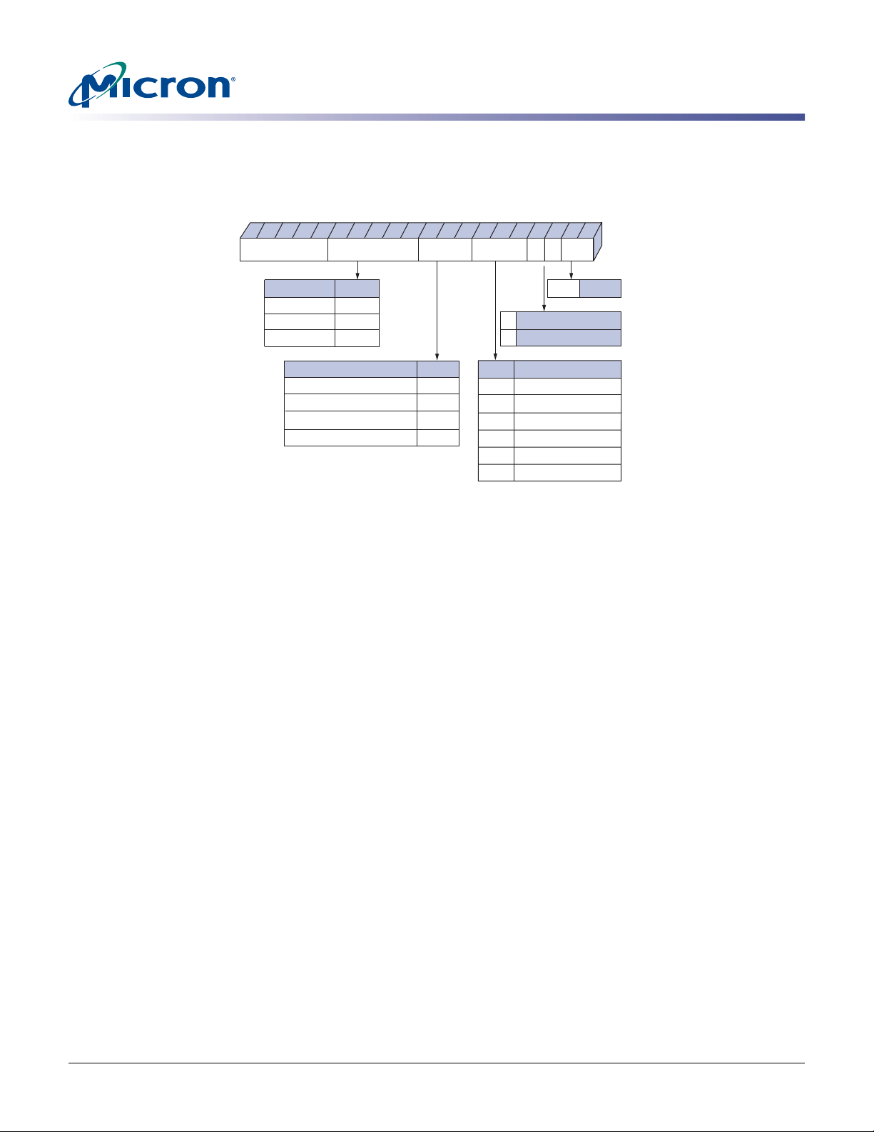
Figure 1: 512Mb DDR2 Part Numbers
Example Part Number: MT47H64M8BT-37E :A
MT47H Package Speed
Configuration
128 Meg x 4
64 Meg x 8
32 Meg x 16
Configuration
128M4
64M8
32M16
512Mb: x4, x8, x16 DDR2 SDRAM
Part Numbers
-
:
Revision
{
:A/:B/:D
L
Low-Power
IT
Industrial Temperature
Revision
Package
84-Ball 12 x 12.5 FBGA
84-Ball 10 x 12.5 FBGA
60-Ball 12 x 10 FBGA
60-Ball 10 x 10 FBGA
Note: Not all speeds and configurations are available. Contact Micron sales for current revision.
FBGA Part Marking Decoder
Due to space limitations, FBGA-packaged components have an abbreviated part
marking that is different from the part number. Micron’s FBGA Part Marking Decoder is
available at www.micron.com/decoder.
General Description
The 512Mb DDR2 SDRAM is a high-speed CMOS, dynamic random access memory
containing 536,870,912 bits. It is internally configured as a 4-bank DRAM. The functional
block diagrams of the all device configurations are shown in “Func ti onal Description”
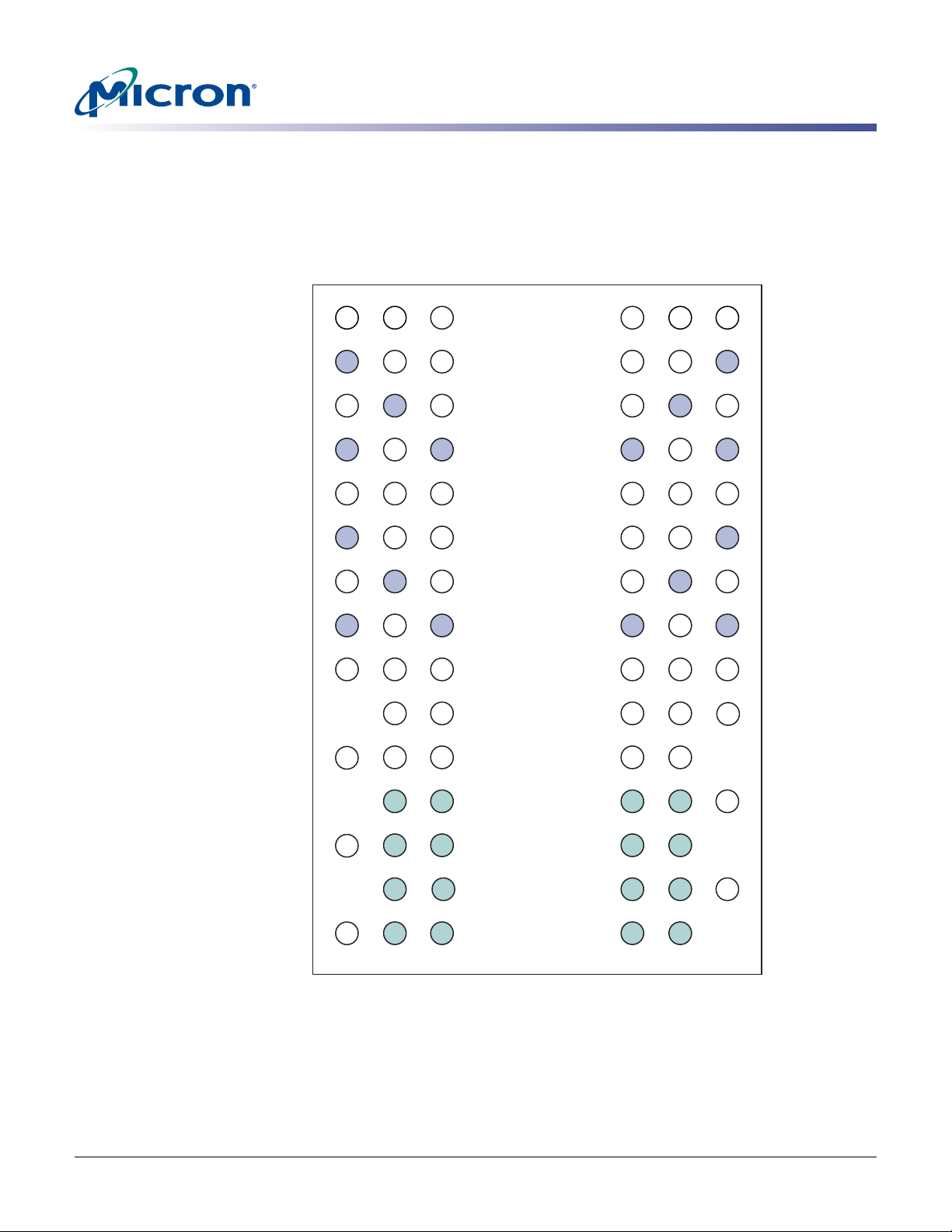
on page 14. Ball assignments and signal de sc riptions are shown in “ B al l A ssignme nt and
Description” on page 9.
CC
BN
CB
B6
Speed Grade
t
CK = 5ns, CL = 3
-5E
t
CK = 3.75ns, CL = 4
-37E
t
CK = 3ns, CL = 5
-3
t
CK = 3ns, CL = 4
-3E
t
CK = 2.5ns, CL = 6
-25
t
CK = 2.5ns, CL = 5
-25E
The 512Mb DDR2 SDRAM uses a double data rate architecture to achieve high-speed
operation. The double data rate architecture is essentially a 4n-prefetch architecture,
with an interface designed to transfer two data words per clock cycle at the I/O balls. A
single read or write access for the 512Mb DDR2 SDRAM effectively consists of a single
4n-bit-wide, one-clock-cycle data transfer at the internal DRAM core and four corresponding n-bit-wide, one-half-clock-cycle data transfers at the I/O balls.
A bidirectional data strobe (DQS, DQS#) is transmitted externally, along with data, for
use in data capture at the receiver. DQS is a strobe transmitted by the DDR2 SDRAM
during READs and by the memory controller during WRITEs. DQS is edge-aligned with
data for READs and center-aligned with data for WRITEs. The x16 offering has two data
strobes, one for the lower byte (LDQS, LDQS#) and one for the upper byte (UDQS,
UDQS#).
PDF: 09005aef8117c18e, Source: 09005aef8211b2e6 Micron Technology, Inc., reserves the right to change products or specifications without notice.
512MbDDR2_2.fm - R ev. K 8/06 EN
7 ©2004 Micron Technology, Inc. All rights reserved.
Page 8

512Mb: x4, x8, x16 DDR2 SDRAM
General Description
The 512Mb DDR2 SDRAM operates from a differential clock (CK and CK#); the crossing
of CK going HIGH and CK# going LOW will be referred to as the positive edge of CK.
Commands (address and control signals) are registered at every positive edge of CK.
Input data is registered on both edges of DQS, and output data is referenced to both
edges of DQS as well as to both edges of CK.
Read and write accesses to the DDR2 SDRAM are burst-oriented; accesses start at a
selected location and continue for a programmed number of locat ions in a programme d
sequence. Accesses begin with the registration of an ACTIVE command, which is then
followed by a READ or WRITE command. The address bits registered coincident with the
ACTIVE command are used to select the bank and row to be accessed. The address bits
registered coinci dent with the READ or WR ITE command are us ed to select the bank and
the starting column location for the burst access.
The DDR2 SDRAM provides for programmable read or write burst lengths of four or
eight locations. DDR2 SDRAM supports interrupting a burst read of eight with another
read or a burst write of eight with another write. An au to precharge function may be
enabled to provide a self-timed row precharge that is initiated at the end of the burst
access.
As with standard DDR SDRAMs, the pipeline d, multibank ar chitectur e of DDR2 SDRAMs
allows for concurrent operation, thereby providing high, effective bandwidth by hiding
row precharge and activation time.
A self refresh mode is provided, along with a power-saving, power-down mode.
All inputs are compatible with the JEDEC standard for SSTL_18. All full drive-strength
outputs are SSTL_18-compatible.
Industrial Temperature
The industrial temperature (IT) device has two simultaneous requirements: ambient
temperature surrounding the device cannot exceed –40°C or +85°C, and the case
temperature cannot exceed –40°C or 95°C. JEDEC specifications require the refresh rate
to double when T
refresh option. Additionally, ODT resistance and the input/output impedance must be
derated when the T
General Notes
• The functionality and the timing specifications discussed in this data sheet are for the
DLL-enabled mode of operation.
• Throughout the data sheet, the various figures and text refer to DQs as “DQ.” The DQ
term is to be interpreted as any and all DQ collectively, unless specifically stated
otherwise. Additionally, the x16 is divided into 2 bytes, the lower byte and upper byte.
For the lower byte (DQ0–DQ7), DM refers to LDM and DQS refers to LDQS. For the
upper byte (DQ8–DQ15), DM refers to UDM and DQS refers to UDQS.
• Complete functionality is described throughout the document, and any page or
diagram may have been simplified to convey a topic and may not be inclusive of all
requirements.
• Any specific requirement takes precedence over a general statement.
exceeds 85°C; this also requires use of the high-temperature self
C
is < 0°C or > 85°C.
C
PDF: 09005aef8117c18e, Source: 09005aef8211b2e6 Micron Technology, Inc., reserves the right to change products or specifications without notice.
512MbDDR2_2.fm - R ev. K 8/06 EN
8 ©2004 Micron Technology, Inc. All rights reserved.
Page 9
Ball Assignment and Description
Figure 2: 84-Ball FBGA (x16)
12mm x 12.5mm and 10mm x 12.5mm (top view)
1234 67895
A
B
C
D
E
F
G
H
K
L
M
N
P
R
VDD
DQ14
DDQ
V
DQ12
V
DQ6
V
DDQ
DQ4
J
V
RFU
V
VDD
DD
DDL
SS
NC
V
SSQ
DQ9
V
SSQ
NC
V
SSQ
DQ1
V
SSQ
REF
V
CKE
BA0
A10
A3
A7
A12
UDM
V
DQ11
LDM
V
DQ3
WE#
V
DDQ
V
DDQ
V
BA1
A1
A5
A9
RFU
512Mb: x4, x8, x16 DDR2 SDRAM
Ball Assignment and Description
SS
SS
SS
SSQ
V
UDQS
V
DDQ
DQ10
V
SSQ
LDQS
V
DDQ
DQ2
SSDL
V
RAS#
CAS#
A2
A6
A11
RFU
UDQS#/NU
V
SSQ
DQ8
V
SSQ
LDQS#/NU
V
SSQ
DQ0
V
SSQ
CK
CK#
CS#
A0
A4
A8
RFU
V
DDQ
DQ15
DDQ
V
DQ13
V
DDQ
DQ7
V
DDQ
DQ5
DD
V
ODT
V
DD
VSS
PDF: 09005aef8117c18e, Source: 09005aef8211b2e6 Micron Technology, Inc., reserves the right to change products or specifications without notice.
512MbDDR2_2.fm - R ev. K 8/06 EN
9 ©2004 Micron Technology, Inc. All rights reserved.
Page 10
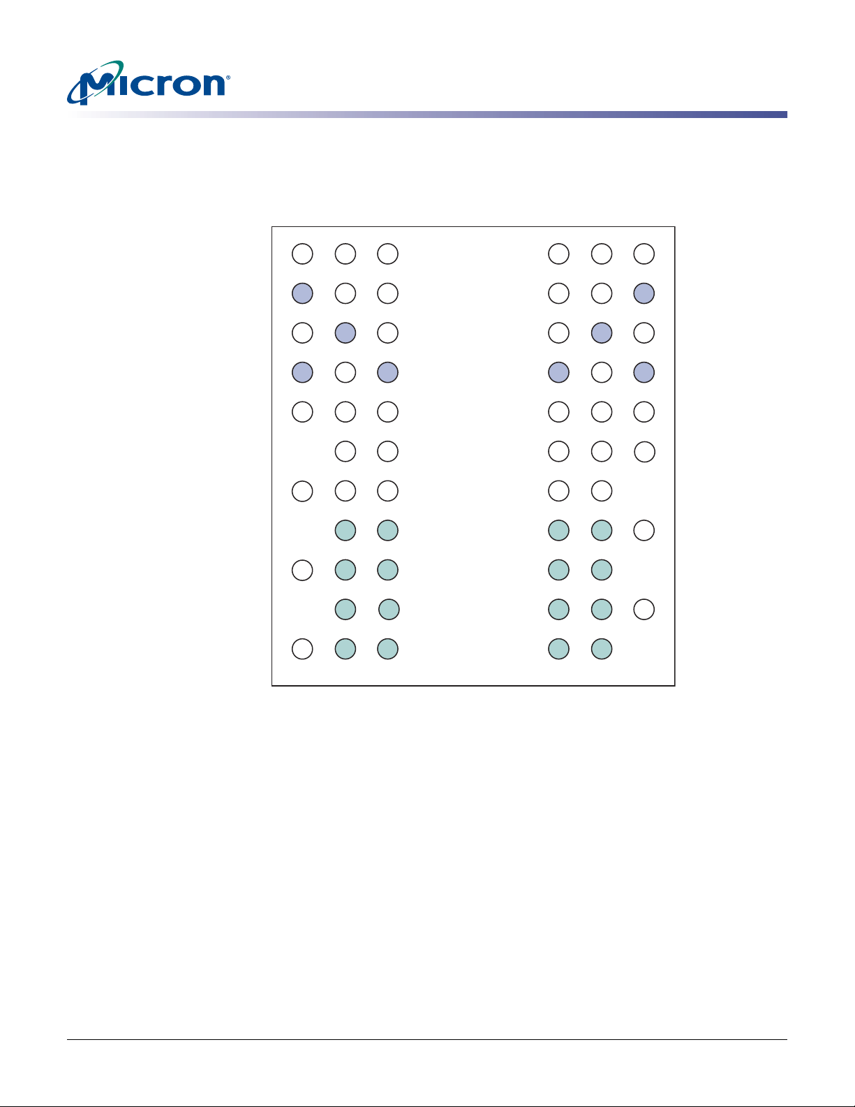
Figure 3: 60-Ball FBGA (x4, x8)
12mm x 10mm and 10mm x 10mm (top view)
A
VDD
B
NF, DQ6
C
V
D
NF, DQ4
E
V
F
G
RFU
H
J
K
L
VDD
1234 67895
SS
DM, DM/RDQS
SSQ
REF
V
VDDQ
DQ3
V
SS
WE#
BA1
A1
A5
A9
RFU
NF, RDQS#/NU
DDQ
DDL
V
SS
VSSQ
DQ1
V
V
CKE
BA0
A10
A3
A7
A12
512Mb: x4, x8, x16 DDR2 SDRAM
Ball Assignment and Description
SSQ
DQS#/NU
V
DQS
V
DDQ
DQ2
V
SSDL
RAS#
CAS#
A2
A6
A11
RFU
V
SSQ
DQ0
V
SSQ
CK
CK#
CS#
A0
A4
A8
A13
VDDQ
NF, DQ7
DDQ
V
NF, DQ5
V
DD
ODT
V
DD
VSS
PDF: 09005aef8117c18e, Source: 09005aef8211b2e6 Micron Technology, Inc., reserves the right to change products or specifications without notice.
512MbDDR2_2.fm - R ev. K 8/06 EN
10 ©2004 Micron Technology, Inc. All rights reserved.
Page 11
512Mb: x4, x8, x16 DDR2 SDRAM
Ball Assignment and Description
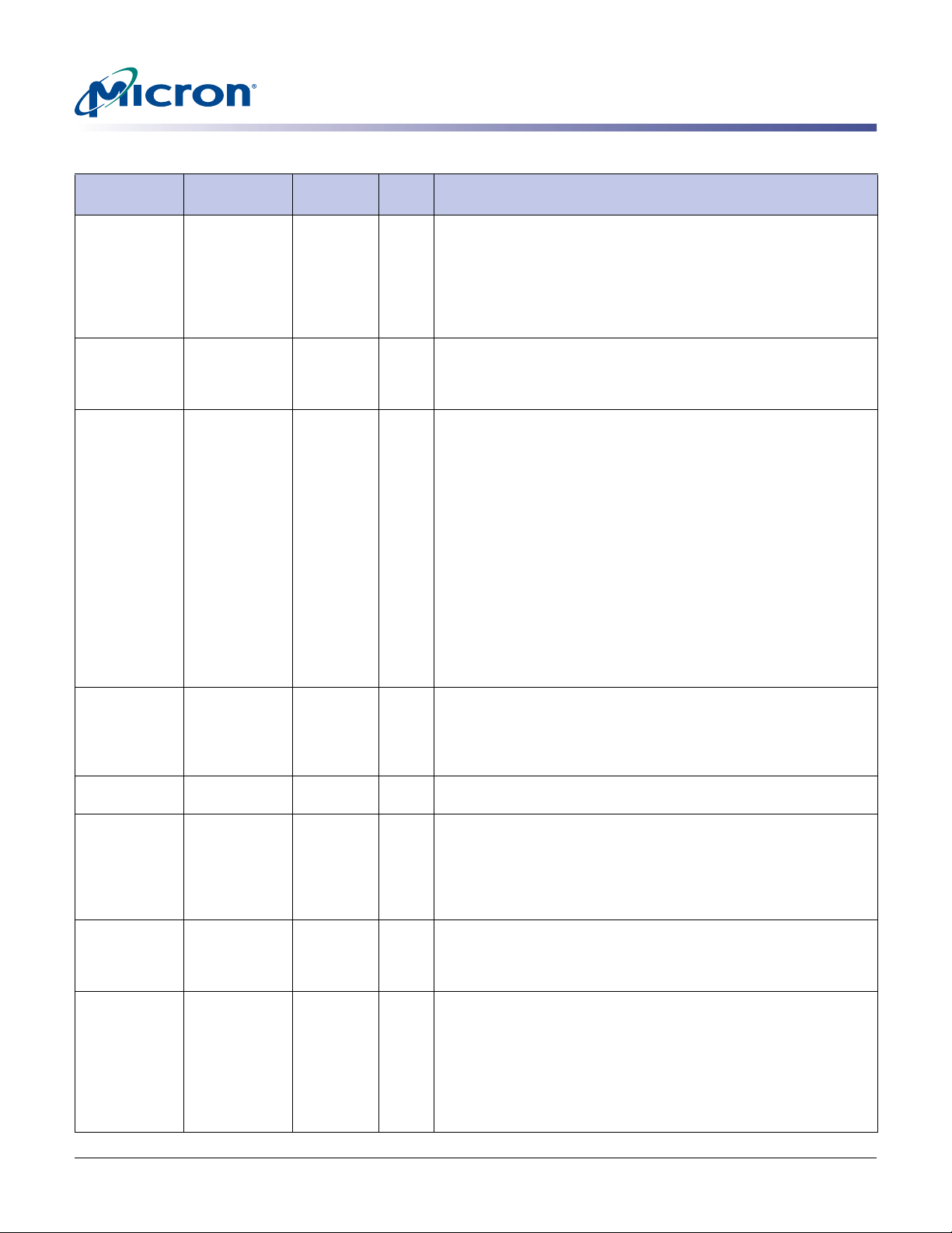
Table 3: FBGA 84-/60-Ball Descriptions – 128 Meg x 4, 64 Meg x 8, 32 Meg x 16
x16 FBGA Ball
Number
x4, x8 FBGA
Ball Number Symbol Type Description
K9 F9 ODT Input
J8, K8 E8, F8 CK, CK# Input
K2 F2 CKE Input
L8 G8 CS# Input
K7, L7,
K3
F3, B3
F7, G7,
F3
B3
RAS#, CAS#,
WE#
LDM, UDM
(DM)
L2, L3 G2, G3 BA0–BA1 Input
M8, M3, M7, N2,
N8, N3, N7, P2,
P8, P3, M2, P7,
R2
–A0–A3
A4–A7
A8–A11
A12
Input
Input
Input
On-die termination: ODT (registered HIGH) enables termination
resistance internal to the DD R2 SDRAM. When enabled, ODT is only
applied to each of the following balls: DQ0–DQ15, LDM, UDM,
LDQS, LDQS#, UDQS, and UDQS# for the x16; DQ0–DQ7, DQS,
DQS#, RDQS, RDQS#, and DM for the x8; DQ0–DQ3, DQS, DQS#,
and DM for the x4. The ODT input will be ignored if disabled via
the LOAD MODE command.
Clock: CK and CK# are differential clock inputs. All address and
control input signals are sampled on the crossing of the positive
edge of CK and negative edge of CK#. Output data (DQs and DQS/
DQS#) is referenced to the crossings of CK and CK#.
Clock enable: CKE (registered HIGH) activates and CKE (registered
LOW) deactivates clocking circuitry on the DDR2 SDRAM. The
specific circuitry that is enabled/disabled is dependent on the DDR2
SDRAM configuration and operating mode. CKE LOW pr ovides
precharge power-down mode and SELF REFRESH operation (all
banks idle), or active power-down (row active in any bank). CKE is
synchronous for power-down entry, power-down exit, output
disable, and for self refresh entry. CKE is asynchronous for SELF
REFRESH exit. Input buffers (excluding CK, CK#, CKE, and ODT) are
disabled during power-down. Input buffers (excluding CKE) are
disabled during self refresh. CKE is an SSTL_18 input but will detect
a LVCMOS LOW level once V
DD is applied during first power-up.
After VREF has become stable during the power on and
initialization sequence, it must be maintained for proper operation
of the CKE receiver. For proper SELF REFRESH operation, V
REF must
be maintained.
Chip select: CS# enables (registered LOW) and disables (registered
HIGH) the command decoder. All commands are masked when CS#
is registered HIGH. CS# provides for external bank selection on
systems with multiple ranks. CS# is considered part of the command
code.
Command inputs: RAS#, CAS#, and WE# (along with CS#) define the
command being entered.
Input data mask: DM is an input mask signal for write data. Input
data is masked when DM is concurrently sampled HIGH during a
WRITE access. DM is sampled on both edges of DQS. Although DM
balls are input-only, the DM loading is designed to match that of
DQ and DQS balls. LDM is DM for lower byte DQ0–DQ7 and UDM is
DM for upper byte DQ8–DQ15.
Bank address inputs: BA0–BA1 define to which bank an ACTIVE,
READ, WRITE, or PRECHARGE command is being applied. BA0–
BA1define which mode register including MR, EMR, EMR(2), and
EMR(3) is loaded during the LOAD MODE command.
Address inputs: Provide the row address for ACTIVE commands, and
the column address and auto precharge bit (A10) for READ/WRITE
commands, to select one location out of the memory array in the
respective bank. A10 sampled during a PRECHARGE command
determines whether the PRECHARGE applies to one bank (A10
LOW, bank selected by BA1–BA0) or all banks (A10 HIGH). The
address inputs also provide the op-code during a LOAD MODE
command.
PDF: 09005aef8117c18e, Source: 09005aef8211b2e6 Micron Technology, Inc., reserves the right to change products or specifications without notice.
512MbDDR2_2.fm - R ev. K 8/06 EN
11 ©2004 Micron Technology, Inc. All rights reserved.
Page 12
512Mb: x4, x8, x16 DDR2 SDRAM
Ball Assignment and Description
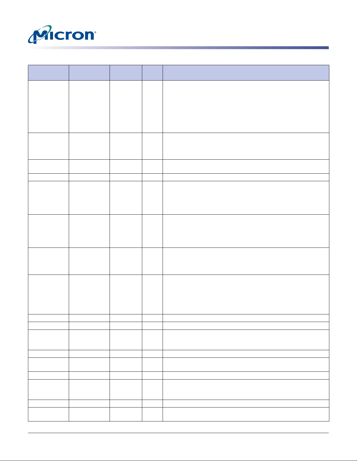
Table 3: FBGA 84-/60-Ball Descriptions – 128 Meg x 4, 64 Meg x 8, 32 Meg x 16 (continued)
x16 FBGA Ball
Number
x4, x8 FBGA
Ball Number Symbol Type Description
– H8, H3, H7, J2,
J8, J3, J7, K2,
G8, G2, H7, H3,
H1, H9, F1, F9,
C8, C2, D7, D3,
D1, D9, B1, B9
– C8, C2, D7, D3,
K8, K3, H2, K7,
L2, L8
–DQ0–DQ3
D1, D9, B1, B9
A8–A11
A12–A13
DQ4–DQ7
DQ8–DQ11
DQ12–DQ15
DQ0–DQ3
DQ4–DQ7
– C8,C2,D7,D3 DQ0–DQ3 I/O
B7
– UDQS,
A8
F7
– LDQS,
E8
– B7, A8 DQS, DQS# I/O
–B3A2RDQS,
A1, E1, M9, J9, R1
A1, E9, H9, L1 VDD Supply
J1 E1 V
A9, C1, C3, C7,
C9, E9, G1, G3,
A9, C1,
C3, C7, C9
G7, G9
J2 E2 V
A3, E3, J3, N1, P9A3, E3, J1, K9 V
A0–A3
Input
A4–A7
UDQS#
LDQS#
Output
RDQS#
DDL Supply
DDQ Supply
V
REF Supply
SS Supply
Address inputs: Provide the row address for ACTIVE commands and
the column address and auto precharge bit (A10) for READ/WRITE
commands to select one location out of the memory array in the
respective bank. A10 sampled during a PRECHARGE command
determines whether the PRECHARGE applies to one bank (A10
LOW, bank selected by BA1–BA0) or all banks (A10 HIGH). The
address inputs also provide the op-code during a LOAD MODE
command.
I/O
Data input/output: Bidirectional data bus for 32 Meg x 16.
I/O
Data input/output: Bidirectional data bus for 64 Meg x 8.
Data input/output: Bidirectional data bus for 128 Meg x 4.
I/O
Data strobe for upper byte: Output with read data, input with
write data for source synchronous operation. Edge-aligned with
read data, center-aligned with write data. UDQS# is only used
when differential data strobe mode is enabled via the LOAD MODE
command.
I/O
Data strobe for lower byte: Output with read data, input with write
data for source synchronous operation. Edge-aligned with read
data, center-aligned with write data. LDQS# is only used when
differential data strobe mode is enabled via the LOAD MODE
command.
Data strobe: Output with read data, input with write data for
source synchronous operation. Edge-aligned with read data, center
aligned with write data. DQS# is only used when differential data
strobe mode is enabled via the LOAD MODE command.
Redundant data strobe for 64 Meg x 8 only. RDQS is enabled/
disabled via the LOAD MODE command to the extended mode
register (EMR). When RDQS is enabled, RDQS is output with read
data only and is ignored during wr ite data. When RDQS is disabled,
ball B3 becomes data mask (see DM ball). RDQS# is only used when
RDQS is enabled and differential data strobe mode is enabled.
Power supply: 1.8V ±0.1V.
DLL power supply: 1.8V ±0.1V.
DQ power supply: 1.8V ±0.1V. Isolated on the device for improved
noise immunity.
SSTL_18 reference voltage.
Ground.
J7 E7 V
A7, B2, B8, D2,
D8, E7, F2, F8,
A7, B2,
B8, D2, D8
SSDL Supply
V
SSQ Supply
DLL ground. Isolated on the device from V
SS and VSSQ.
DQ ground. Isolated on the device for improved noise immunity.
H2, H8
A2, E2 – NC –
– B1, D1, D9, B9 NF –
No connect: These balls should be left unconnected.
No function: These balls are used as DQ4–DQ7 on the 64 Meg x 8,
but are NF (no function) on the 128 Meg x 4 configuration.
PDF: 09005aef8117c18e, Source: 09005aef8211b2e6 Micron Technology, Inc., reserves the right to change products or specifications without notice.
512MbDDR2_2.fm - R ev. K 8/06 EN
12 ©2004 Micron Technology, Inc. All rights reserved.
Page 13
512Mb: x4, x8, x16 DDR2 SDRAM
Ball Assignment and Description
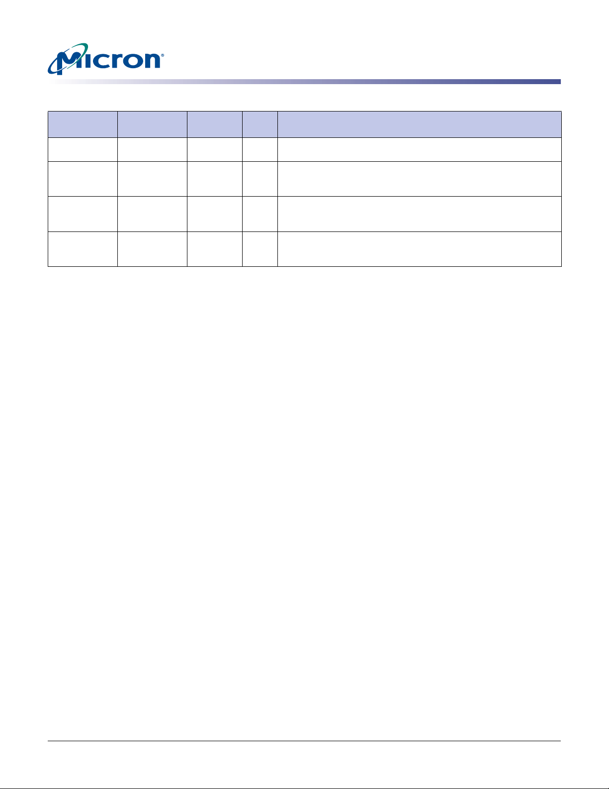
Table 3: FBGA 84-/60-Ball Descriptions – 128 Meg x 4, 64 Meg x 8, 32 Meg x 16 (continued)
x16 FBGA Ball
Number
x4, x8 FBGA
Ball Number Symbol Type Description
A8, E8 – NU –
– A2, A8 NU –
L1, R3, R7, R8 – RFU –
– G1, L3, L7 RFU –
Not used: Not used only on x16. If EMR[E10] = 0, A8 and E8 are
UDQS# and LDQS#. If EMR[E10] = 1, then A8 and E8 are not used.
Not used: Not used only on x8. If EMR[E10] = 0, A2 and A8 are
RDQS# and DQS#.
If EMR[E10] = 1, then A2 and A8 are not used.
Reserved for future use (x16 only): Row address bits A13 (R8), A14
(R3), and A15 (R7) are reserved for 2Gb and 4Gb densities. BA2 (L1)
is reserved for 1Gb device.
Reserved for future use (x4, x8 only): Row address bits A14 (L3) and
A15 (L7) are reserved for 2Gb and 4Gb densities. BA2 (G1) is
reserved for 1Gb device.
PDF: 09005aef8117c18e, Source: 09005aef8211b2e6 Micron Technology, Inc., reserves the right to change products or specifications without notice.
512MbDDR2_2.fm - R ev. K 8/06 EN
13 ©2004 Micron Technology, Inc. All rights reserved.
Page 14
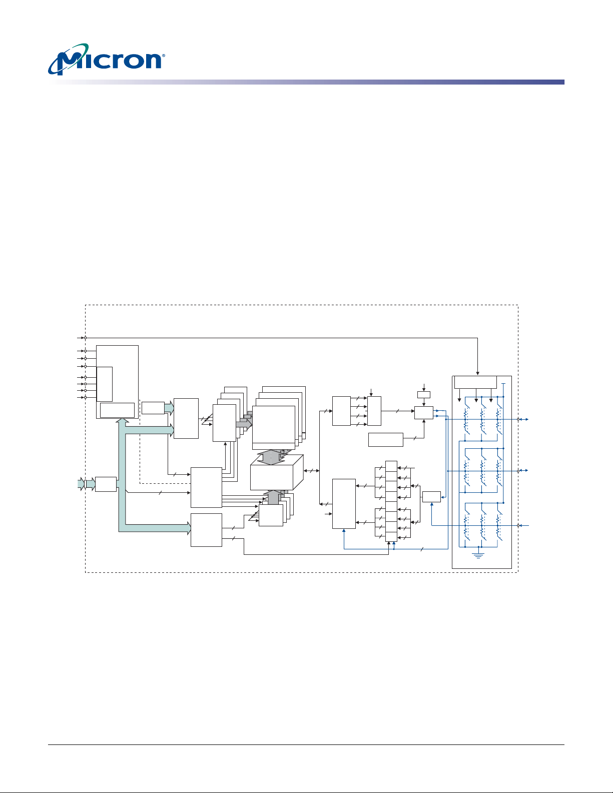
Functional Description
The 512Mb DDR2 SDRAM is a high-speed CMOS dynamic random access memory
containing 536,870,912 bits. The 512Mb DDR2 SDRAM is internally configured as a 4bank DRAM.
The 512Mb DDR2 SDRAM uses a double data rate architecture to achieve high-speed
operation. The DDR2 architectur e is essentially a 4n-pr efetch architectur e , with an interface designed to transfer two data words per clock cycle at the I/O balls. A single read or
write access for the 512Mb DDR2 SDRAM consists of a single 4n-bit-wide, one-clockcycle data transfer at the internal DRAM core and four corr esponding n-bit- wide, one-
half-clock-cycle data transfers at the I/O balls.
Prior to normal operation, the DDR2 SDRAM must be i n itialized. The following sections
provide detailed information covering device initialization, register definition,
command descriptions, and device operation.
Figure 4: Functional Block Diagram – 32 Meg x 16
ODT
CKE
CK
CK#
CS#
RAS#
CAS#
WE#
A0–A12,
BA0, BA1
15
CONTROL
DECODE
COMMAND
MODE
REGISTERS
ADDRESS
REGISTER
LOGIC
15
REFRESH
COUNTER
13
10
13
2
ROW-
ADDRESS
MUX
2
13
ADDRESS
DECODER
BANK
CONTROL
LOGIC
COLUMN-
ADDRESS
COUNTER/
LATCH
BANK 3
BANK 2
BANK 1
BANK 0
ROW-
LATCH&
8,192
8
2
BANK 3
BANK 2
BANK 1
BANK 0
MEMORY
ARRAY
(8,192 x 128 x 64)
SENSE AMPLIFIERS
16,384
I/O GATING
DM MASK LOGIC
256
(x64)
COLUMN
DECODER
64
Internal
CK, CK#
COL0, COL1
512Mb: x4, x8, x16 DDR2 SDRAM
Functional Description
sw2
sw2
R2
R2
sw2
R2
R2
sw2
R2
R2
VssQ
sw3
sw3
sw3
sw3
VDDQ
R3
R3
R3
R3
R3
R3
DQ0–DQ15
UDQS, UDQS#
LDQS, LDQS#
UDM, LDM
ODT CONTROL
sw1
sw1
R1
R1
sw1
R1
R1
sw1
R1
R1
16
DATA
2
2
2
16
16
16
16
CK, CK#
DLL
DRVRS
4
UDQS, UDQS#
LDQS, LDQS#
2
2
RCVRS
16
4
COL0, COL1
16
64
READ
LATCH
WRITE
FIFO
&
DRIVERS
CK OUT
CK IN
16
16
16
8
MASK
64
DATA
MUX
DQS
GENERATOR
INPUT
REGISTERS
2
2
2
2
16
16
16
16
64
PDF: 09005aef8117c18e, Source: 09005aef8211b2e6 Micron Technology, Inc., reserves the right to change products or specifications without notice.
512MbDDR2_2.fm - R ev. K 8/06 EN
14 ©2004 Micron Technology, Inc. All rights reserved.
Page 15
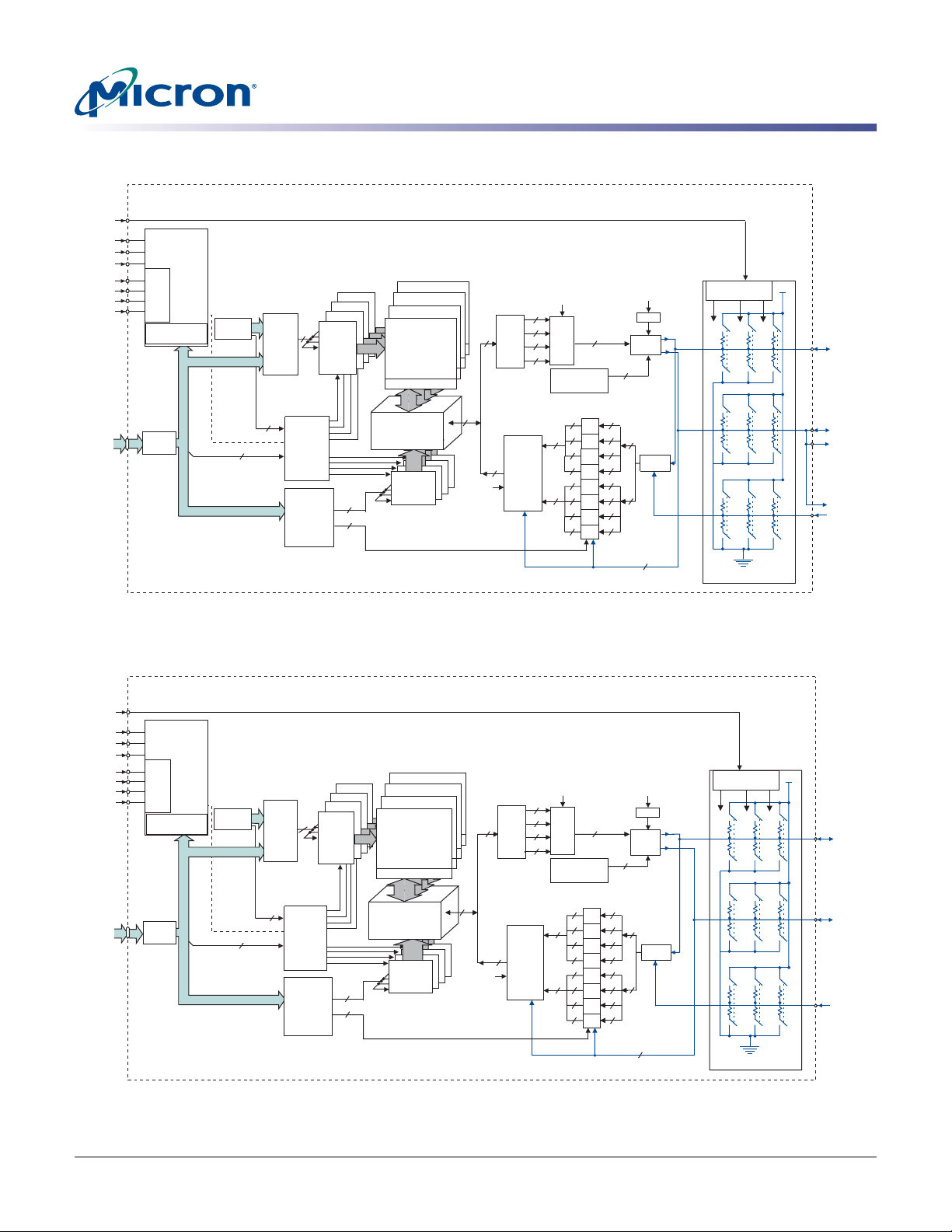
Figure 5: Functional Block Diagram – 64 Meg x 8
ODT
16
CONTROL
LOGIC
DECODE
COMMAND
MODE
REGISTERS
ADDRESS
REGISTER
BANK 3
BANK 2
REFRESH
14
COUNTER
16
14
ROW-
ADDRESS
MUX
2
2
10
14
BANK
CONTROL
LOGIC
COLUMN-
ADDRESS
COUNTER/
LATCH
BANK 1
BANK 0
ROW-
ADDRESS
LATCH &
DECODER
16,384
8
2
BANK 3
BANK 2
BANK 1
BANK 0
MEMORY
ARRAY
(16,384 x 256 x 32)
SENSE AMPLIFIERS
8,192
I/O GATING
DM MASK LOGIC
256
(x32)
COLUMN
DECODER
32
internal
CK, CK#
COL0, COL1
CKE
CK
CK#
CS#
RAS#
CAS#
WE#
A0–A13,
BA0, BA1
512Mb: x4, x8, x16 DDR2 SDRAM
Functional Description
ODT CONTROL
sw1
sw1
R1
R1
sw1
R1
R1
sw1
R1
R1
8
CK, CK#
DLL
DRVRS
2
DQS, DQS#
1
1
1
1
RCVRS
1
8
8
8
8
8
COL0, COL1
8
32
READ
LATCH
WRITE
DRIVERS
CK OUT
FIFO
&
CK IN
8
8
8
MASK
DATA
MUX
DATA
DQS
GENERATOR
INPUT
REGISTERS
1
1
4
1
1
8
32
8
8
8
32
sw2
sw2
R2
R2
sw2
R2
R2
sw2
R2
R2
sw3
sw3
sw3
sw3
VDDQ
R3
R3
R3
R3
R3
R3
DQ0–DQ7
DQS, DQS#
RDQS#
RDQS
DM
Figure 6: Functional Block Diagram – 128 Meg x 4
ODT
16
CONTROL
LOGIC
DECODE
COMMAND
MODE
REGISTERS
ADDRESS
REGISTER
BANK3
BANK2
REFRESH
14
COUNTER
16
14
ROW-
ADDRESS
MUX
2
2
11
14
BANK
CONTROL
LOGIC
COLUMN-
ADDRESS
COUNTER/
LATCH
BANK1
BANK0
ROW-
ADDRESS
LATCH &
DECODER
16,384
9
2
BANK3
BANK2
BANK1
BANK0
MEMORY
ARRAY
(16,384 x 512 x 16)
SENSE AMPLIFIERS
8,192
I/O GATING
DM MASK LOGIC
512
(x16)
COLUMN
DECODER
16
internal
CK, CK#
COL0, COL1
CKE
CK
CK#
CS#
RAS#
CAS#
WE#
A0–A13,
BA0, BA1
16
READ
LATCH
16
WRITE
FIFO
&
DRIVERS
CK OUT
CK IN
COL0, COL1
4
4
MUX
4
4
GENERATOR
4
MASK
16
DATA
4
DATA
DQS
INPUT
REGISTERS
1
1
1
1
4
4
4
4
CK, CK#
DLL
DRVRS
2
DQS, DQS#
1
1
1
1
1
4
4
4
4
4
2
2
RCVRS
VssQ
ODT CONTROL
sw1
sw2
sw1
sw2
R1
R2
R1
R2
sw1
sw2
R1
R2
R1
R2
sw1
sw2
R1
R2
R1
R2
VssQ
sw3
sw3
sw3
sw3
VDDQ
R3
R3
R3
R3
R3
R3
DQ0–DQ3
DQS, DQS#
DM
PDF: 09005aef8117c18e, Source: 09005aef8211b2e6 Micron Technology, Inc., reserves the right to change products or specifications without notice.
512MbDDR2_2.fm - R ev. K 8/06 EN
15 ©2004 Micron Technology, Inc. All rights reserved.
Page 16
PDF: 09005aef8117c18e, Source: 09005aef8211b2e6 Micron Technology, Inc., reserves the right to change products or specifications without notice.
512MbDDR2_2.fm - Rev. K 8/06 EN
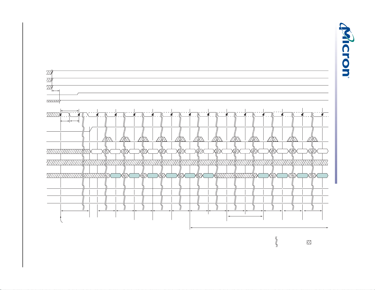
Initialization
DDR2 SDRAMs must be powered up and initialized in a predefined manner. Operational procedures other than
those specified may result in undefined operation. Figure7 illustrates the sequence required for power-up and
initialization.
Figure 7: DDR2 Power-up and Initialization
Notes appear on page 17
VDD
VDDL
VDDQ
VTT
VREF
CK#
CK
CKE
1
t
VTD
LVCMOS
LOW LEVEL
1
T0
t
CL
SSTL_18
2
LOW LEVEL
t
CK
t
CL
2
Ta0
Tb0
Tc0Td0
Te0 Tf0
Tg0 Th0 Ti0 Tj0
Tk0 Tl0 Tm0
16 ©2004 Micron Technology, Inc. All rights reserved.
ODT
COMMAND
DM
ADDRESS
DQS
DQ
3
4
3
High-Z
4
High-Z
4
High-Z
R
TT
T = 200µs (MIN)
Power-up:
DD
and stable
V
clock (CK, CK#)
NOP
T = 400ns
(MIN)
5
PRE
A10 = 1
6
t
RPA
LM
CODE
EMR(2)
7
t
MRD
LM
CODE
EMR(3)
8
t
MRD
9
LM
CODE CODE
EMR
t
MRD
LM
MR with
DLL RESET
RFC
MR without
DLL RESET
LM
CODE
13
t
10
PRE
11
REF
12
REF
A10 = 1
t
MRD
t
RPA
200 cycles of CK are required before a READ command can be issued.
t
RFC
t
See note 12
LM
CODE
MRD
EMR with
OCD Default
Indicates a break in
time scale
14
t
MRD
15
LM
CODE
EMR with
OCD Exit
t
MRD
VALID
VALID
Normal
Operation
DON’T CARE
16
512Mb: x4, x8, x16 DDR2 SDRAM
Initialization
Page 17

512Mb: x4, x8, x16 DDR2 SDRAM
Initialization
Notes: 1.
10. Issue a LOAD MODE command for DLL RESET. 200 cycles of clock input is required to lock
11. Issue PRECHARGE ALL command.
12. Issue two or more REFRESH commands.
Applying power; if CKE is maintained below 0.2 x VDDQ,
outputs remain disabled. To guarantee RTT (ODT resistance) is off, VREF must be valid and a low le vel must be applied to the
ODT ball (all other inputs may be undefined; I/Os and outputs must be less than VDDQ during voltage ramp time to avoid DDR2 SDRAM device latch-up). V
TT is not applied directly to
the device; however, tVTT should be ≥0 to avoid device latch-up. At least one of the following two sets of conditions (A or B) must be met to obtain a stable supply state (stable supply
defined as V
DD, VDDL, VDDQ, VREF, and VTT are between their minimum and maximum val-
ues as stated in Table 20 on page 84):
A. Single power source: The VDD voltage ramp from 300mV to VDD (MIN) must take no
longer than 200ms; during the VDD voltage ramp, |VDD - VDDQ| ≤ 0.3V. Once supply voltage
ramping is complete (when VDDQ crosses VDD [MIN]), Table 20 specifications apply.
DD, VDDL, and VDDQ are driven from a single power converter output
• V
• VTT is limited to 0.95V MAX
• VREF tracks VDDQ/2; VREF must be within ±0.3V with respect to VDDQ/2 during supply ramp time
DDQ ≥ VREF at all times
• V
B. Multiple power sources: VDD ≥ VDDL ≥ VDDQ must be maintained during supply volt-
age ramping, for both AC and DC levels, until supply voltage ramping completes (V
DDQ
crosses VDD [MIN]). Once supply voltage ramping is complete, Table 20 specifications apply.
• Apply VDD and VDDL before or at the same time as VDDQ; VDD/VDDL voltage ramp
time must be ≤200ms from when V
DD ramps from 300mV to VDD (MIN)
• Apply VDDQ before or at the same time as VTT; the VDDQ voltage ramp time from
when VDD (MIN) is achieved to when VDDQ (MIN) is achieved must be ≤500ms; while
DD is ramping, current can be supplied from VDD through the device to VDDQ
V
• VREF must track VDDQ/2; VREF must be within ±0.3V with respect to VDDQ/2 during
supply ramp time; VDDQ ≥ VREF must be met at all times
• Apply V
TT; the VTT voltage ramp time from when VDDQ (MIN) is achieved to when
VTT (MIN) is achieved must be no greater than 500ms
2. CKE uses LVCMOS input levels prior to state T0 to ensure DQs are High-Z during device
power-up prior to V
REF being stable. After state T0, CKE is required to have SSTL_18 input
levels. Once CKE transitions to a high level, it must stay HIGH for the duration of the initial-
ization sequence.
3. PRE = PRECHARGE command, LM = LOAD MODE command, MR = Mode Register, EMR =
extended mode register, EMR2 = extended mode register 2, EMR3 = extended mode register 3, REF = REFRESH command, ACT = ACTIVE command, A10 = PRECHARGE ALL, CODE =
desired values for mode registers (bank addresses are required to be decoded), VALID - any
valid command/address, RA = row address, bank address.
4. DM represents DM for x4, x8 configurations and UDM, LDM for x16 configuration; DQS represents DQS, DQS#, UDQS, UDQS #, LDQS, LDQS#, RDQS, RDQS# for the appropriate configuration (x4, x8, x16); DQ represents DQ0–DQ3 for x4, DQ–DQ7 for x8, and DQ0–DQ15 for x16.
5. For a minimum of 200µs after stable power and clock (CK, CK#), apply NOP or DESELECT
commands, then take CKE HIGH.
6. Wait a minimum of 400ns, then issue a PRECHARGE ALL command.
7. Issue a LOAD MODE command to the EMR(2). (T o issue an EMR(2) co mman d, provide LOW
to BA0, and provide HIGH to BA1.) Set register E7 to “0” or “1;” all others must be “0.”
8. Issue a LOAD MODE command to the EMR(3). (T o issue an EMR(3) command, provide HIGH
to BA0 and BA1.) Set all registers to “0.”
9. Issue a LOAD MODE command to the EMR to enable DLL. To issue a DLL ENABLE command,
provide LOW to BA1 and A0; provide HIGH to BA0. Bits E7, E8, and E9 can be set to “0” or
“1;” Micron recommends setting them to “0.”
the DLL. (To issue a DLL RESET, provide HIGH to A8 and provide LOW to BA1 and BA0.) CKE
must be HIGH the entire time.
PDF: 09005aef8117c18e, Source: 09005aef8211b2e6 Micron Technology, Inc., reserves the right to change products or specifications without notice.
512MbDDR2_2.fm - R ev. K 8/06 EN
17 ©2004 Micron Technology, Inc. All rights reserved.
Page 18

512Mb: x4, x8, x16 DDR2 SDRAM
Initialization
13. Issue a LOAD MODE command with LOW to A8 to initialize device operation (i.e., to program operating parameters without resetting the DLL). To access the mode registers, BA1
=1, BA0 = 0.
14. Issue a LOAD MODE command to the EMR to enable OCD default by setting bits E7, E8, and
E9 to “1,” and then setting all other desired parameters. To access the extended mode register, BA1 = 0, BA0 = 1.
15. Issue a LOAD MODE command to the EMR to enable OCD exit by setting bits E7, E8, and E9
to “0,” and then setting all other desired parameters. To access the extended mode registers, BA1 = 0, BA0 = 1.
16. The DDR2 SDRAM is now initialized and ready for normal operation 200 clock cycles after
the DLL RESET at Tf0. It is also suggested to include a single dummy WRITE command followed by
mand to the DRAM.
t
WR anytime after the REFRESH commands, but before the first true WRITE com-
PDF: 09005aef8117c18e, Source: 09005aef8211b2e6 Micron Technology, Inc., reserves the right to change products or specifications without notice.
512MbDDR2_2.fm - R ev. K 8/06 EN
18 ©2004 Micron Technology, Inc. All rights reserved.
Page 19

Mode Register (MR)
The mode register is used to define the specific mode of oper atio n of the DDR2 SDRAM.
This definition includes the selection of a burst length, burst type, CAS latency, operating mode, DLL RESET, write recovery, and power-down mode, as shown in Figure8 on
page 20. Contents of the mode register can be altered by re-executing the LOAD MODE
(LM) command. If the user chooses to modify only a subset of the MR variables, all variables (M0–M13 for x4 and x8 or M0–M12 for x16) must be programmed when the
command is issued.
The MR is programmed via the LM command (bits BA1–BA0 = 0, 0) and othe r bits (M13–
M0 for x4 and x8, M12–M0 for x16) will retain the stored information until it is
programmed again or the device loses power (except for bit M8, which is self-clearing).
Reprogramming the mode register will not alter the contents of the memory array,
provided it is performed correctly.
The LM command can only be issued (or reissued) when all banks are in the precharged
state (idle state) and no bursts are in progress. The control ler must wait the specified
time
Violating either of these requirements will result in unspecified operation.
Burst Length
512Mb: x4, x8, x16 DDR2 SDRAM
Mode Register (MR)
t
MRD before initiating any subsequent operations such as an ACTIVE command.
Burst length is defined by bits M0–M3, as shown in Figure 8 on page 20. Read and write
accesses to the DDR2 SDRAM are burst-oriented, with the burst length being programmable to either four or eight. The burst length dete rmines the maximum number of
column locations that can be accessed for a given READ or WRITE command.
When a READ or WRITE command is issued, a block of columns equal to the burst
length is effectively selected. All accesses for that burst take place within this block,
meaning that the burst will wrap within the block if a boundary is reached. The block is
uniquely selected by A2–Ai when BL = 4 and by A3–Ai when BL = 8 (where Ai is the most
significant column address bit for a given configuration). The remaining (least significant) address bit(s) is (are) used to select the starting location within the block. The
programmed burst length applies to both READ and WRITE bursts.
PDF: 09005aef8117c18e, Source: 09005aef8211b2e6 Micron Technology, Inc., reserves the right to change products or specifications without notice.
512MbDDR2_2.fm - R ev. K 8/06 EN
19 ©2004 Micron Technology, Inc. All rights reserved.
Page 20
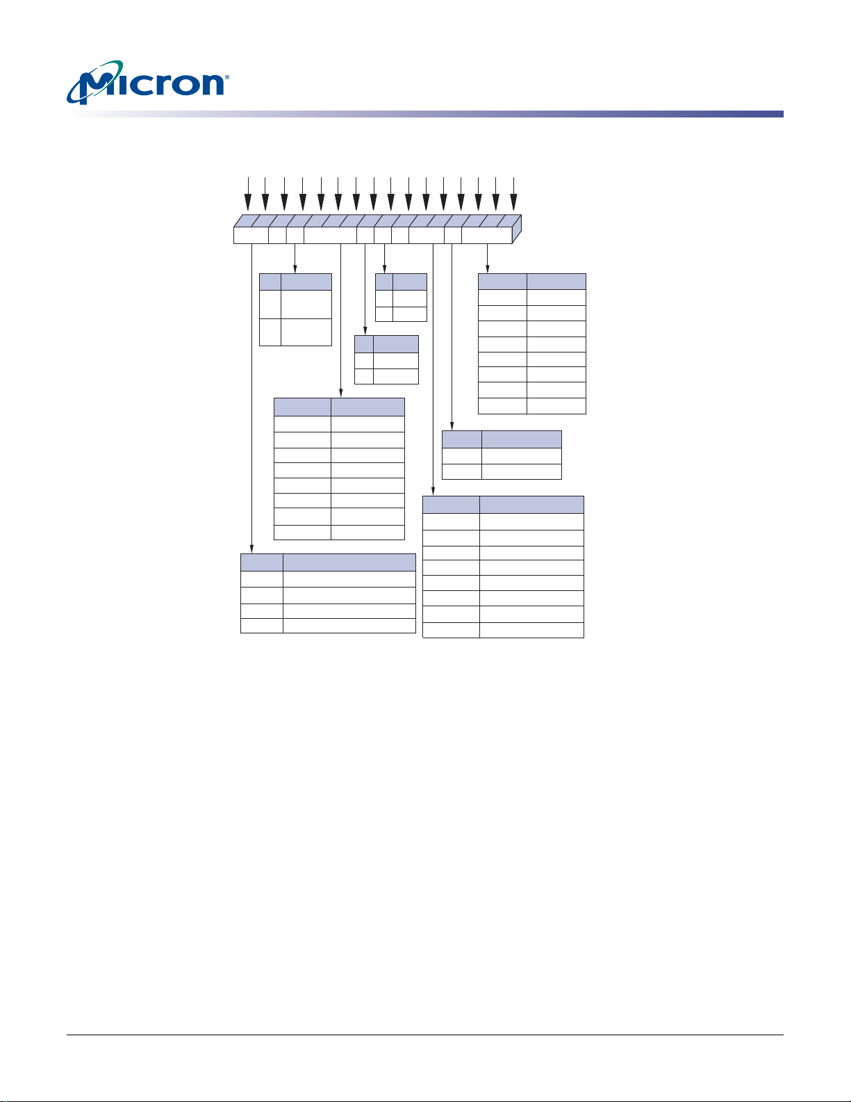
Figure 8: Mode Register (MR) Definition
512Mb: x4, x8, x16 DDR2 SDRAM
Mode Register (MR)
15
MR
BA1
M15
A13
14
1
0
M12
PD mode
0
(Normal)
1
Slow Exit
(Low Power)
M11
0
0
0
0
1
1
1
1
M14
0
0
1
Extended Mode Register (EMR)
0
0
Extended Mode Register (EMR2)
1
1
Extended Mode Register (EMR3)
1
A10A12 A11BA0
10111213
WR
Fast Exit
WRITE RECOVERY
M9
M10
0
0
1
0
0
1
1
1
0
0
1
0
0
1
1
1
Mode Register Definition
Mode Register (MR)
A9 A7 A6 A5 A4 A3A8 A2 A1 A0
976 5438 210
CAS#
DLL TM
M7
DLL Reset
M8
0
1
Reserved
2
3
4
5
6
Reserved
Reserved
0
1
Latency
Mode
Normal
Test
No
Yes
M6
0
0
0
0
1
1
1
1
Burst Length
BTPD
M3
0
1
M4
M5
0
0
1
0
0
1
1
1
0
0
1
0
0
1
1
1
M0
M1
M2
0
0
0
1
0
0
0
1
0
1
1
0
0
0
1
1
0
1
0
1
1
1
1
1
Burst Type
Sequential
Interleaved
CAS Latency (CL)
Reserved
Reserved
Reserved
Reserved
Address Bus
Mode Register (Mx)
Burst Length
Reserved
Reserved
4
8
Reserved
Reserved
Reserved
Reserved
3
4
5
6
Notes: 1. M13 (A13) is reserved for future use and must be programmed to “0.” A13 is not used in
x16 configuration.
2. Not all listed CL options are supported in any individual speed grade.
Burst Type
Accesses within a given burst may be programme d to be either seque ntial or interl eaved.
The burst type is selected via bit M3, as shown in Figure8. The ordering of accesses
within a burst is determined by th e burs t leng th, t he burs t t ype, and the starting column
address, as sho wn in Table 4 on page 21. DDR2 SDRAM supports 4-bit burst mode and 8bit burst mode only. For 8-bit burst mode, full, interleaved address ordering is
supported; however, sequential address ordering is nibble-based.
PDF: 09005aef8117c18e, Source: 09005aef8211b2e6 Micron Technology, Inc., reserves the right to change products or specifications without notice.
512MbDDR2_2.fm - R ev. K 8/06 EN
20 ©2004 Micron Technology, Inc. All rights reserved.
Page 21
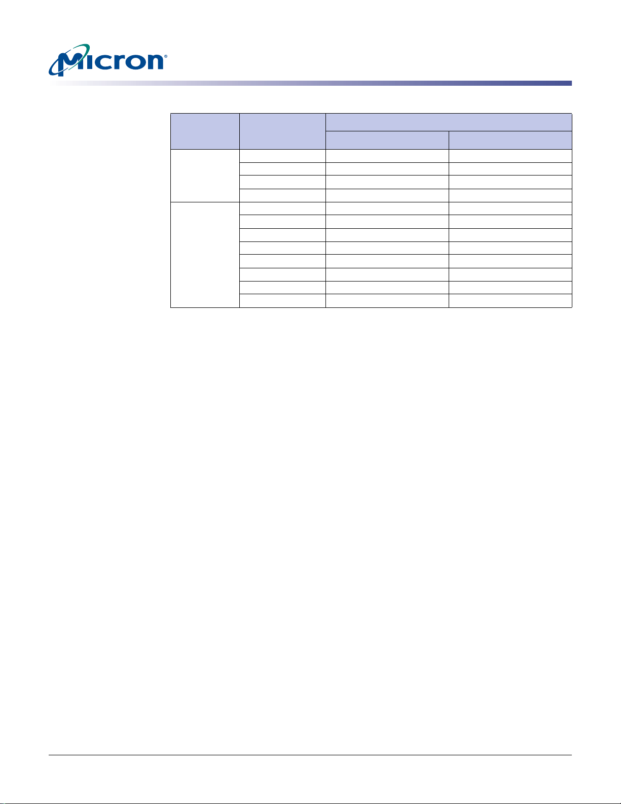
Table 4: Burst Definition
512Mb: x4, x8, x16 DDR2 SDRAM
Mode Register (MR)
Operating Mode
Starting Column
Burst Length
4 0 0 0, 1, 2, 3 0, 1, 2, 3
8 0 0 0 0, 1, 2, 3, 4, 5, 6, 7 0 , 1, 2, 3, 4, 5, 6, 7
Address
(A2, A1, A0)
0 1 1, 2, 3, 0 1, 0, 3, 2
1 0 2, 3, 0, 1 2, 3, 0, 1
1 1 3, 0, 1, 2 3, 2, 1, 0
0 0 1 1, 2, 3, 0, 5, 6, 7, 4 1, 0, 3, 2, 5, 4, 7, 6
0 1 0 2, 3, 0, 1, 6, 7, 4, 5 2, 3, 0, 1, 6, 7, 4, 5
0 1 1 3, 0, 1, 2, 7, 4, 5, 6 3, 2, 1, 0, 7, 6, 5, 4
1 0 0 4, 5, 6, 7, 0, 1, 2, 3 4, 5, 6, 7, 0, 1, 2, 3
1 0 1 5, 6, 7, 4, 1, 2, 3, 0 5, 4, 7, 6, 1, 0, 3, 2
1 1 0 6, 7, 4, 5, 2, 3, 0, 1 6, 7, 4, 5, 2, 3, 0, 1
1 1 1 7, 4, 5, 6, 3, 0, 1, 2 7, 6, 5, 4, 3, 2, 1, 0
Burst Type = Sequential Burst Type = Interleaved
Order of Accesses Within a Burst
The normal operating mode is selected by issuing a command with bit M7 set to “0,” and
all other bits set to the desired values, as shown in Figure 8 on page 20. When bit M7 is
“1,” no other bits of the mode register are programmed. Programming bit M7 to “1”
places the DDR2 SDRAM into a test mode that is only used by the manufacturer and
should not be used. No operation or functionality is guaranteed if M7 bit is “1.”
DLL RESET
Write Recovery
DLL RESET is defined by bit M8, as shown in Figure8 on page 20. Programming bit M8
to “1” will activate the DLL RESET function. Bit M8 is self-clearing, meaning it returns
back to a value of “0” after the DLL RESET function has been issued.
Anytime the DLL RESET function is used, 200 clock cycles must occur before a READ
command can be issued to allow time for the internal clock to be synchronized with the
external clock. Failing to wait for synchronization to occur may result in a violation of
t
the
AC or tDQSCK parameters.
Write recovery (WR) time is defined by bits M9–M11, as shown in Figure 8 on page 20.
The WR register is used by the DDR2 SDRAM during WRITE with auto precharge operation. During WRITE with auto precharge operation, the DDR2 SDRAM delays the
internal auto precharge operation b y WR clocks (programmed in bits M9–M11) from the
last data burst. An example of WRITE with auto precharge is shown in Figure 39 on
page 57.
WR values of 2, 3, 4, 5, or 6 clocks may be used for programming bits M9–M11. The user
is required to program the value of WR, which is calculated b y dividing
onds) by
WR [cycles] =
t
CK (in nanoseconds) and rounding up a noninteger value to the next integer;
t
WR [ns] / tCK [ns]. Reserved states should not be used as unknown opera-
t
WR (in nanosec-
tion or incompatibility with future versions may result.
PDF: 09005aef8117c18e, Source: 09005aef8211b2e6 Micron Technology, Inc., reserves the right to change products or specifications without notice.
512MbDDR2_2.fm - R ev. K 8/06 EN
21 ©2004 Micron Technology, Inc. All rights reserved.
Page 22

Power-Down Mode
512Mb: x4, x8, x16 DDR2 SDRAM
Mode Register (MR)
Active pow er-down (PD) mode is defined by bit M12, as shown in Figure8 on page 20.
PD mode allows the user to determine the active power-down mode, which determines
performance versus power savings. PD mode bit M12 does not apply to precharge PD
mode.
When bit M12 = 0, standard active PD mode, or “fast-exit” active PD mode, is enabled.
t
The
XARD parameter is used for fast-exit active PD exit timing. The DLL is expected to
be enabled and running during this mode.
CAS Latency (CL)
When bit M12 = 1, a lower-power active PD mode, or “slow-exit” active PD mode, is
enabled. The
t
XARDS parameter is used for slow-exit active PD exit timing. The DLL can
be enabled but “frozen” during active PD mode since the exit-to-READ command timing
is relaxed. The power difference expected between PD normal and PD low-power mode
is defined in the I
DD table.
The CAS latency (CL) is defined by bits M4–M6, as shown in Figure 8 on page 20. CL is
the delay , in clock cycles, between the registration of a READ command and the availability of the first bit of output data. The CL can be set to 3, 4, 5, or 6 clocks, depending
on the speed grade option being used.
DDR2 SDRAM does not support any half-clock latencie s. Reserved states should not be
used as unknown operation or incompatibility with future versions may result.
DDR2 SDRAM also supports a feature called posted CAS additive latency (AL). This
feature allows the READ command to be issued prior to
t
RCD (MIN) by delaying the
internal command to the DDR2 SDRAM by AL clocks. The AL feature is described in
more detail in “Posted CAS Additive Latency (AL)” on page 26.
Examples of CL = 3 and CL = 4 are shown in Figure9 on page 23; both assume AL = 0. If a
READ command is registered at clock edge n, and the CL is m clocks, the data will be
available nominally coincident with clock edge n + m (this assumes AL = 0).
PDF: 09005aef8117c18e, Source: 09005aef8211b2e6 Micron Technology, Inc., reserves the right to change products or specifications without notice.
512MbDDR2_2.fm - R ev. K 8/06 EN
22 ©2004 Micron Technology, Inc. All rights reserved.
Page 23
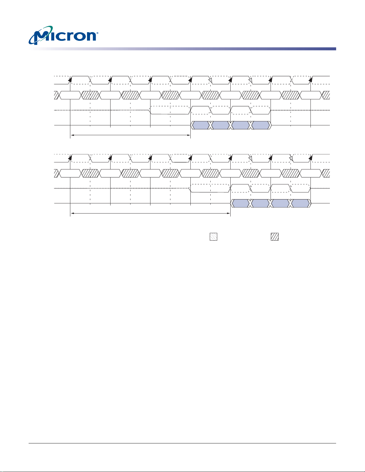
Figure 9: CAS Latency (CL)
512Mb: x4, x8, x16 DDR2 SDRAM
Extended Mode Register (EMR)
CK#
CK
COMMAND
DQS, DQS#
DQ
CK#
CK
COMMAND
DQS, DQS#
DQ
T0 T1 T2
READ
NOP NOP NOP
CL = 3 (AL = 0)
T0 T1 T2
READ
NOP NOP NOP
CL = 4 (AL = 0)
Notes: 1. BL = 4.
2. Posted CAS# additive latency (AL) = 0.
3. Shown with nominal tAC, tDQSCK, and tDQSQ.
T3 T4 T5
NOP NOP
D
D
D
D
OUT
n
OUT
n + 1
OUT
n + 2
OUT
n + 3
T3 T4 T5
NOP NOP
D
D
OUT
n
OUT
n + 1
D
OUT
n + 2
T6
NOP
T6
NOP
D
OUT
n + 3
DON’T CARETRANSITIONING DATA
Extended Mode Register (EMR)
The extended mode register controls functions beyond those controlled by the mode
register; these additional functions are DLL enable/disable, output drive strength, ondie termination (ODT) (R
DQS# enable/disable, RDQS/RDQS# enable/disable, and output disable/ enable. These
functions are controlled via the bits shown in Figure 10 on page 24. The EMR is
programmed via the LM command and will retain the stored information until it is
programmed again or the device loses power. Reprogramming the EMR will not alter the
contents of the memory array, provided it is performed correctly.
The EMR must be loaded when all banks are idle and no bursts are in progress, and the
controller must wait the specif ie d ti me
tion. Violating either of these requiremen ts could result in unspecified operation.
PDF: 09005aef8117c18e, Source: 09005aef8211b2e6 Micron Technology, Inc., reserves the right to change products or specifications without notice.
512MbDDR2_2.fm - R ev. K 8/06 EN
TT), posted AL, off-chip driver impedance calibration (OCD),
t
MRD before initiating any subsequent opera-
23 ©2004 Micron Technology, Inc. All rights reserved.
Page 24
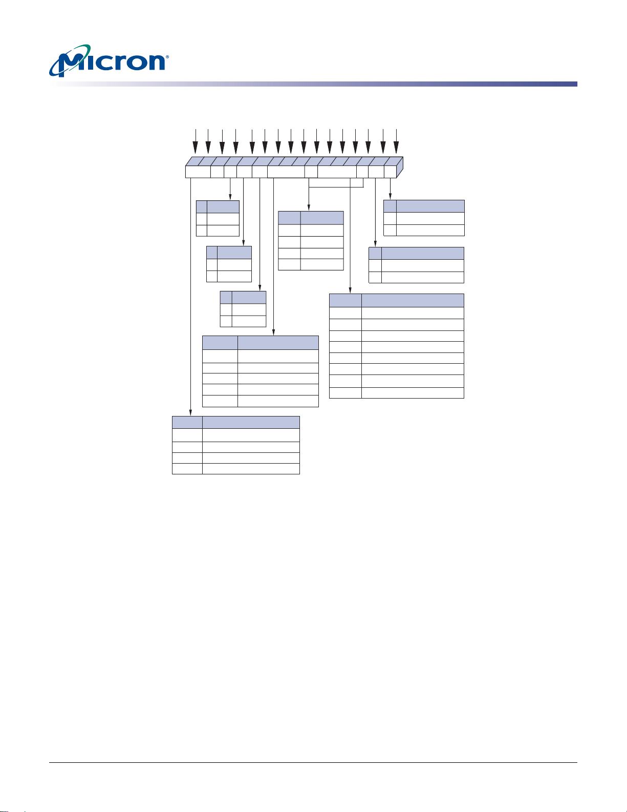
Figure 10: Extended Mode Register Definition
512Mb: x4, x8, x16 DDR2 SDRAM
DLL Enable/Disable
15
MRS
E12
14
0
1
E9
Outputs
Enabled
Disabled
E11
0
1
0
0
0
1
1
A13
2
0
E8
0
0
1
0
1
RDQS
RDQS Enable
No
Yes
E10
DQS# Enable
0
Enable
1
Disable
E7
OCD Operation
0
OCD not supported
1
Reserved
0
Reserved
0
Reserved
1
OCD default state
A10A12 A11BA0BA1
A9 A7 A6 A5 A4 A3A8 A2 A1 A0
976 54 38 210
10111213
DQS#
OCD Program
E6
0
0
1
1
R
Rtt (nominal)
E2
R
TT disabled
0
75Ω
1
150Ω
0
1
1
1
TT
50Ω
RTT
E5
E4
E3
0
0
0
0
0
1
0
1
0
0
1
1
1
0
0
1
0
1
1
1
0
1
1
1
Address Bus
Extended Mode
Register (Ex)
DLLPosted CAS#out
ODS
E0
DLL Enable
0
Enable (Normal)
1
Disable (Test/Debug)
Output Drive Strength
E1
0
Full strength (18Ω target)
1
Reduced strength (40Ω target)
Posted CAS# Additive Latency (AL)
0
1
2
3
4
Reserved
Reserved
Reserved
E15
0
0
1
1
Notes: 1. During initialization, all three bits must be set to “1” for OCD default state, then must be
2. E13 (A13) is not used on the x16 configuration.
DLL Enable/Disable
The DLL may be enabled or disabled by programming bit E0 during the LM command,
as shown in Figure10. The DLL must be enabled for normal operation. DLL enable is
required during power-up initialization and upon returning to normal operation after
having disabled the DLL for the purpose of debugging or evaluation. Enabling the DLL
should always be followed by resetting the DLL using the LM command.
The DLL is automatically disabled when entering SELF REFRESH operation and is automatically re-enabled and reset upon exit of SELF REFRESH oper ation.
Anytime the DLL is enabled (and subsequently reset), 200 clock cycles must occur before
a READ command can be issued, to allow time for the internal clock to synchronize with
the external clock. Failing to wait for synchronization to occur may result in a violation
of the
Mode Register Set
E14
Mode register set (MRS)
0
Extended mode register (EMRS)
1
Extended mode register (EMRS2)
0
Extended mode register (EMRS3)
1
set to “0” before initialization is finished, as detailed in the notes on pages 17–18.
t
AC or tDQSCK parameters.
PDF: 09005aef8117c18e, Source: 09005aef8211b2e6 Micron Technology, Inc., reserves the right to change products or specifications without notice.
512MbDDR2_2.fm - R ev. K 8/06 EN
24 ©2004 Micron Technology, Inc. All rights reserved.
Page 25

Output Drive Strength
The output drive strength is defined by bit E1, as shown in Figure10 on page 24. The
normal drive strength for all outputs are specified to be SSTL_18. Programming bit E1 = 0
selects normal (full strength) drive strength for all outputs. Selecting a r educed drive
strength option (E1 = 1) will reduce all outputs to approximately 60 percent of the
SSTL_18 drive strength. This option is intended for the support of lighter load and/or
point-to-point environments.
DQS# Enable/Disable
The DQS# ball is enabled by bit E10. When E10 = 0, DQS# is the complement of the
differential data strobe pair DQS/DQS#. When disabled (E10 = 1), DQS is used in a
single-ended mode and the DQS# ball is disabled. When disabled, DQS# should be left
floating. This function is also used to enable/disable RDQS#. If RDQS is enabled (E11 =
1) and DQS# is enabled (E10 = 0), then both DQS# and RDQS# will be enabled.
RDQS Enable/Disable
The RDQS ball is enabled by bit E11, as shown in Figure10 on page 24. This feature is
only applicable to the x8 configuration. When enabled (E11 = 1), RDQS is identical in
function and timing to data strobe DQS during a READ. During a WRITE operation,
RDQS is ignored by the DDR2 SDRAM.
512Mb: x4, x8, x16 DDR2 SDRAM
Output Drive Strength
Output Enable/Disable
The OUTPUT ENABLE function is defined by bit E12, as shown in Figure10 on page 24.
When enabled (E12 = 0), all outputs (DQs, DQS, DQS#, RDQS, RDQS#) function
normally. When disabled (E12 = 1), all DDR2 SDRAM outputs (DQs, DQS, DQS#, RDQS,
RDQS#) are disabled, thus removing output buffer current. The output disable featur e i s
intended to be used during I
On-Die Termination (ODT)
ODT effective resistance, RTT (EFF), is defined by bits E2 and E6 of the EMR, as shown in
Figure10 on page 24. The ODT feature is designed to improve signal integrity of the
memory channel by allowing the DDR2 SDRAM controller to independently turn on/off
ODT for any or all devices. R
selectable and apply to each DQ, DQS/DQS#, RDQS/RDQS#, UDQS/UDQS#, LDQS/
LDQS#, DM, and UDM/LDM signals. Bits (E6, E2) deter m ine wh at ODT resistance is
enabled by turning on/off “sw1,” “sw2,” or “sw3.” The ODT effective resistance value is
selected by enabling switch “sw1,” which enables all R1 values that are 150Ω each,
enabling an effective resistance of 75Ω (R
all R2 values that are 300Ω each, enable an effective ODT resistance of 150Ω (R
= R2/2). Switch “sw3” enables R1 values of 100Ω, enabling effective resistance of 50Ω.
Reserved states should not be used, as unknown operation or incompatibility with
future versions may result.
The ODT control ball is used to determine when R
assuming ODT has been enabled via bits E2 and E6 of the EMR. The ODT feature and
ODT input ball are only used during active, active power-down (both fast-exit and slowexit modes), and precharge power-down modes of operation. ODT must be turned off
prior to entering self refresh. During power-up and initialization of the DDR2 SDRAM,
ODT should be disabled until issuing the EMR command to enable the ODT feature, at
DD characterization of read current.
TT effective resistance values of 50Ω, 75Ω, and 150Ω are
TT2 (EFF) = R2/2). Similarly, if “sw2” is enabled,
TT2 (EFF)
TT (EFF) is turned on and off,
PDF: 09005aef8117c18e, Source: 09005aef8211b2e6 Micron Technology, Inc., reserves the right to change products or specifications without notice.
512MbDDR2_2.fm - R ev. K 8/06 EN
25 ©2004 Micron Technology, Inc. All rights reserved.
Page 26
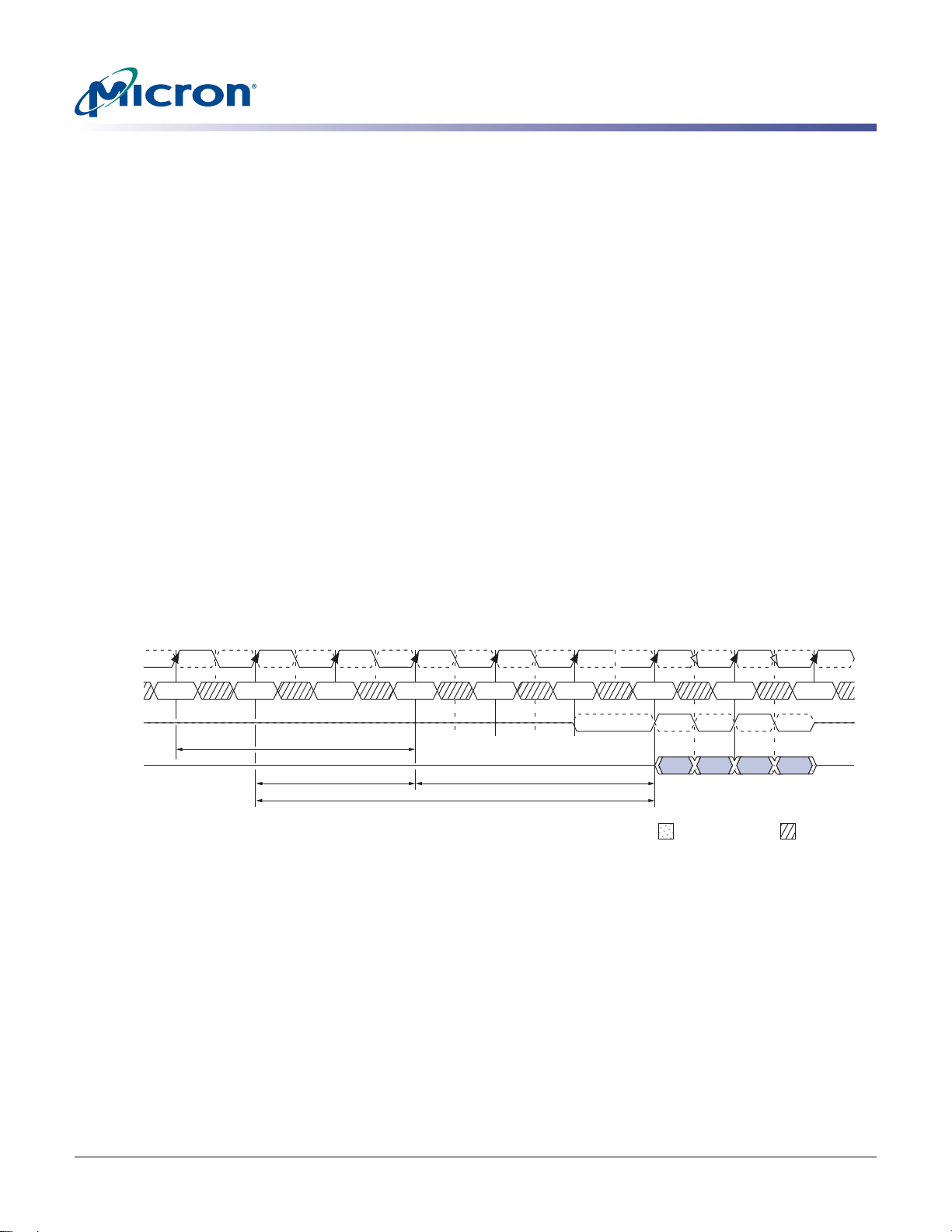
Off-Chip Driver (OCD) Impedance Calibration
which point the ODT ball will determine the RTT (EFF) value. Any time the EMR enables
the ODT function, ODT may not be driven HIGH until eight clocks after the EMR has
been enabled. See “ODT Timing” on page74 for ODT timing diagrams.
Off-Chip Driver (OCD) Impedance Calibration
The OFF-CHIP DRIVER function is no longer supported and must be set to the default
state. See “Initialization” on page 16 for proper setting of OCD defaults.
Posted CAS Additive Latency (AL)
Posted CAS additive latency (AL) is supported to make the command and data bus efficient for sustainable bandwidths in DDR2 SDRAM. Bits E3–E5 define the value of AL, as
shown in Figure10 on page 24. Bits E3–E5 allow the user to program the DDR2 SDRAM
with an inverse AL of 0, 1, 2, 3, or 4 clocks. Reserved states should not be used as
unknown operation or incompatibility with future versions may result.
512Mb: x4, x8, x16 DDR2 SDRAM
In this operation, the DDR2 SDRAM allows a READ or WRITE command to be issued
prior to
using this feature would set AL =
held for the time of the AL before it is issued internally to the DDR2 SDRAM device. RL is
controlled by the sum of AL and CL; RL = AL + CL. Write latency (WL) is equal to RL
minus one clock; WL = AL + CL - 1 x
example of a WL is shown in Figure12 on page 27.
Figure 11: READ Latency
T0 T1 T2
CK#
CK
COMMAND
DQS, DQS#
DQ
ACTIVE n
READ n NOP NOP
t
Notes: 1. BL = 4.
2. Shown with nominal
3. CL = 3.
4. AL = 2.
5. RL = AL +CL = 5.
RCD (MIN)
t
RCD (MIN) with the requirement that AL ≤ tRCD (MIN). A typical application
T3 T4 T5
AL = 2
RL = 5
t
AC, tDQSCK, and tDQSQ.
t
RCD (MIN) - 1 x tCK. The READ or WRITE command is
t
CK. An example of RL is shown in Figure11. An
NOP
CL = 3
NOP
T6
NOP
DOUT
n
T7 T8
NOP NOP
DOUT
DOUT
n + 2
n + 1
DOUT
n + 3
DON’T CARETRANSITIONING DATA
PDF: 09005aef8117c18e, Source: 09005aef8211b2e6 Micron Technology, Inc., reserves the right to change products or specifications without notice.
512MbDDR2_2.fm - R ev. K 8/06 EN
26 ©2004 Micron Technology, Inc. All rights reserved.
Page 27
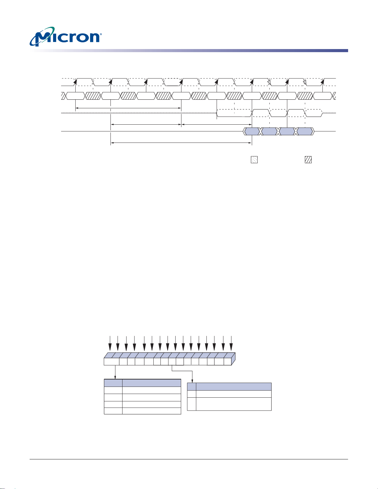
Figure 12: WRITE Latency
512Mb: x4, x8, x16 DDR2 SDRAM
Extended Mode Register 2
CK#
COMMAND
DQS, DQS#
T0 T1 T2
CK
ACTIVE n
DQ
t
RCD (MIN)
NOP NOP
AL = 2 CL - 1 = 2
Notes: 1. BL = 4.
2. CL = 3.
3. AL = 2.
4. WL = AL + CL - 1 = 4.
Extended Mode Register 2
The extended mode register 2 (EMR2) controls functions beyond those controlled by the
mode register. Currently all bits in EMR2 are reserved, except for E7, which is for
commercial or high-temperature operations, as shown in F igure13. The EMR2 is
programmed via the LM command and will retain the stored information until it is
programmed again or the device loses power. Reprogramming the EMR will not alter the
contents of the memory array, provided it is performed correctly.
T3 T4 T5
NOPWRITE n
WL = AL + CL - 1 = 4
NOP
D
n
T6
NOP
D
D
IN
n + 1
IN
IN
n + 2
n + 3
T7
NOP
D
IN
DON’T CARETRANSITIONING DATA
Bit E7 (A7) must be programmed as “1” to provide a faster refresh rate on IT devices if the
T
CASE exceeds 85°C.
EMR2 must be loaded when all banks are idle and no bursts are in progress, and the
controller must wait the specif ie d ti me
tion. Violating either of these requiremen ts could result in unspecified operation.
Figure 13: Extended Mode Register 2 (EMR2) Definition
A9 A7 A6 A5 A4 A3A8 A2 A1 A0
A13
1415
1
EMR2
M15
0
0
1
1
0
0
Mode Register Definition
M14
0
1
Extended mode register (EMR)
0
Extended mode register (EMR2)
1
Extended mode register (EMR3)
Notes: 1. E13 (A13)–E8 (A8) and E6 (A6)–E0 (A0) are reserved for future use and must all be pro-
grammed to “0.” A13 is not used in x16 configuration.
A10A12 A11BA0BA1
976543821 0
10111213
1010101010101010101010101
High Temperature Self Refresh rate enable
Mode register (MR)
E7
Commercial temperature default
0
Industrial temperature option;
1
use if T
t
MRD before initiating any subsequent opera-
Address Bus
Extended Mode
Register (Ex)
exceeds 85°C
C
PDF: 09005aef8117c18e, Source: 09005aef8211b2e6 Micron Technology, Inc., reserves the right to change products or specifications without notice.
512MbDDR2_2.fm - R ev. K 8/06 EN
27 ©2004 Micron Technology, Inc. All rights reserved.
Page 28
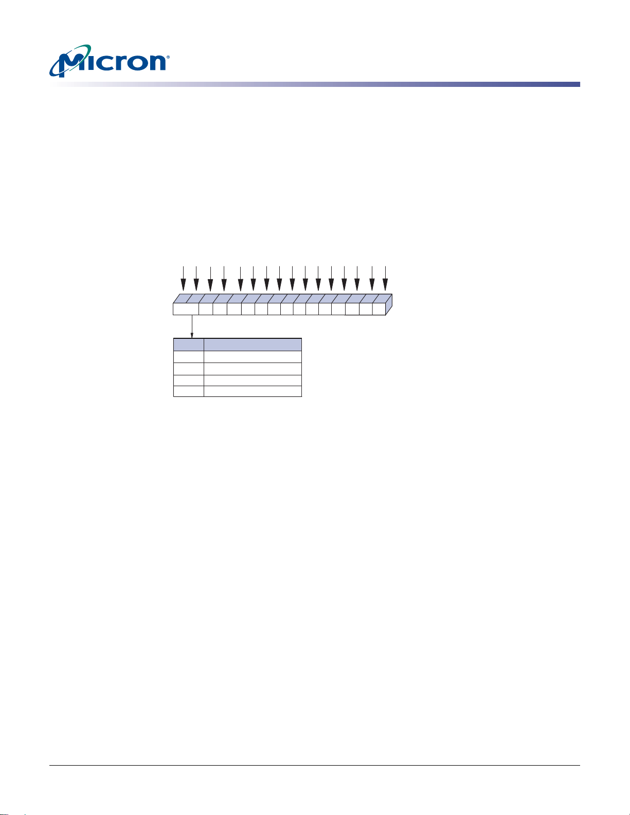
Extended Mode Register 3
The extended mode register 3 (EMR3) controls functions beyond those controlled by the
mode register. Currently all bits in EMR3 are reserved, as shown in Figure14 on page 28.
The EMR3 is programmed via the LM command and will retain the stored information
until it is programmed again or the device loses po wer. Reprogramming the EMR will not
alter the contents of the memory array, provided it is performed correctly.
512Mb: x4, x8, x16 DDR2 SDRAM
Extended Mode Register 3
EMR3 must be loaded when all banks are idle and no bursts are in progress, and the
controller must wait the specif ie d ti me
tion. Violating either of these requiremen ts could result in unspecified operation.
Figure 14: Extended Mode Register 3 (EMR3) Definition
A9 A7 A6 A5 A4 A3A8 A2 A1 A0
A13
1
EMR3
M15
0
0
1
1
0101010101010101010101010
0
Mode Register Definition
M14
0
1
Extended mode register (EMR)
0
Extended mode register (EMR2)
1
Extended mode register (EMR3)
Notes: 1. E13 (A13)–E0 (A0) are reserved for future use and must all be programmed to “0.” A13 is
not used in x16 configuration.
A10A12 A11BA0BA1
976543821 0
101112131415
Mode register (MR)
t
MRD before initiating any subsequent opera-
Address Bus
Extended Mode
Register (Ex)
1
PDF: 09005aef8117c18e, Source: 09005aef8211b2e6 Micron Technology, Inc., reserves the right to change products or specifications without notice.
512MbDDR2_2.fm - R ev. K 8/06 EN
28 ©2004 Micron Technology, Inc. All rights reserved.
Page 29
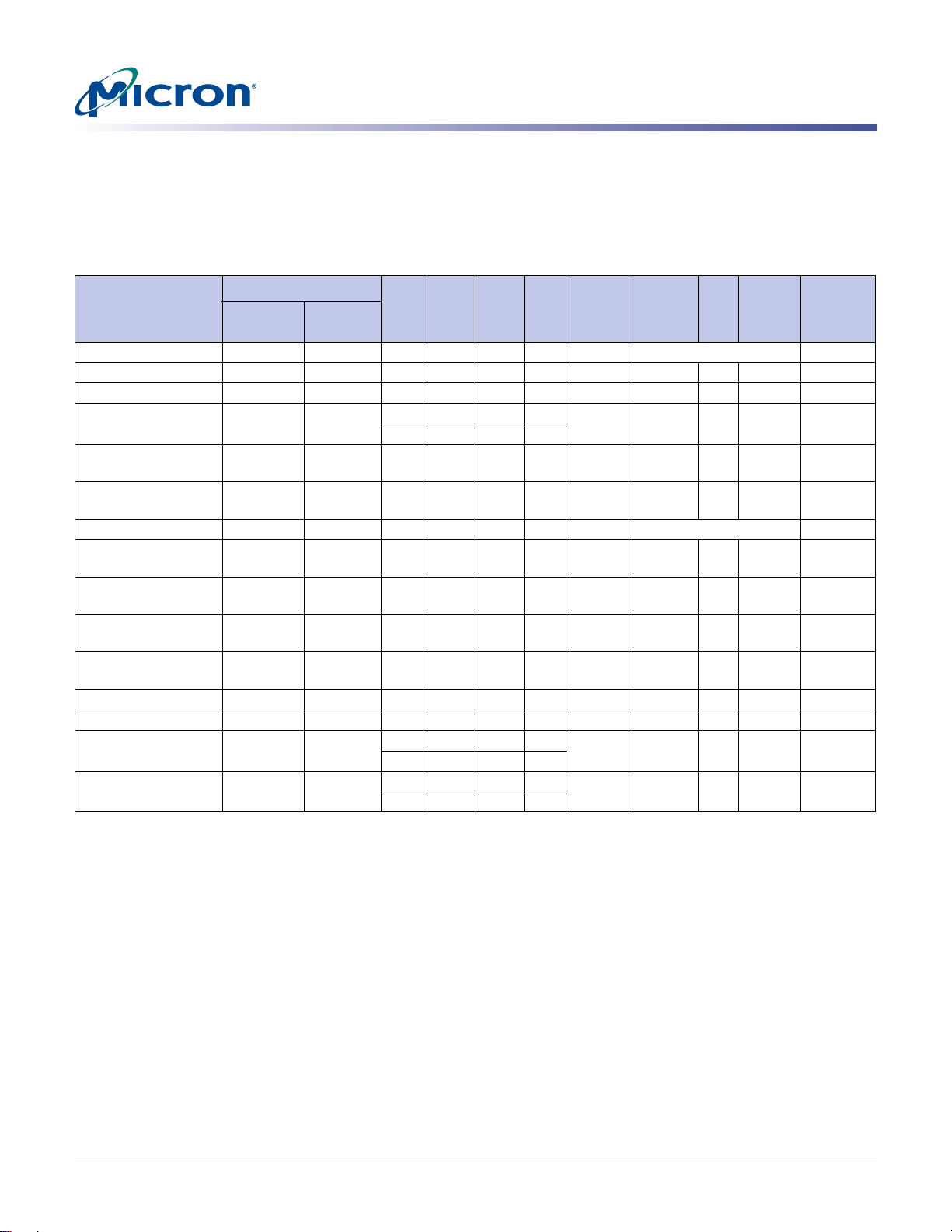
Command Truth Tables
The following tables provide a quick reference of DDR2 SDRAM available commands,
including CKE power-down modes, and bank-to-bank commands.
Table 5: Truth Table – DDR2 Commands
Notes: 1, 5, and 6 apply to all
512Mb: x4, x8, x16 DDR2 SDRAM
Command Truth Tables
Function
LOAD MODE
REFRESH
SELF REFRESH entry
SELF REFRESH exit
Single bank
PRECHARGE
All banks
PRECHARGE
Bank activate
WRITE
WRITE with auto
precharge
READ
READ with auto
precharge
NO OPERATION
Device DESELECT
Power-down entry
Power-down exit
CKE
Previous
Cycle
H H L L L L BA OP Code 2
HHLLLHXXXX
HLLLLHXXXX
LH
HHLLHLBAXLX2
HHLLHLXXHX
H H L L H H BA Row Address
HHLHLLBA
HHLHLLBA
HHLHLHBA
HHLHLHBA
HXLHHHXXXX
HXHXXXXXXX
HL
LH
Current
Cycle
CS# RAS# CAS# WE#
HXXX
LHHH
HXXX
LHHH
HXXX
LHHH
BA1
BA0
XXXX 7
XXXX 4
XXXX 4
A13,
A12,
A11
Column
Address
Column
Address
Column
Address
Column
Address
A10 A9–A0 Notes
Column
L
H
L
H
Address
Column
Address
Column
Address
Column
Address
2, 3
2, 3
2, 3
2, 3
Notes: 1. All DDR2 SDRAM commands are defined by states of CS#, RAS#, CAS#, WE#, and CKE at the
rising edge of the clock.
2. Bank addresses (BA) BA0–BA1 determine which bank is to be operated upon. BA duri ng a
LM command selects which mode register is programmed.
3. Burst reads or writes at BL = 4 cannot be terminated or interrupted. See Figure 21 on
page 40 and Figure 35 on page 53 for other restrictions and details.
4. The power-down mode does not perform any REFRESH operations. The duration of powerdown is limited by the refresh requirements outlined in the AC parametric section.
5. The state of ODT does not affect the states described in this table. The ODT function is not
available during self refresh. See “ODT Timing” on page74 for details.
6. “X” means “H or L” (but a defined logic level).
7. SELF REFRESH exit is asynchronous.
PDF: 09005aef8117c18e, Source: 09005aef8211b2e6 Micron Technology, Inc., reserves the right to change products or specifications without notice.
512MbDDR2_2.fm - R ev. K 8/06 EN
29 ©2004 Micron Technology, Inc. All rights reserved.
Page 30
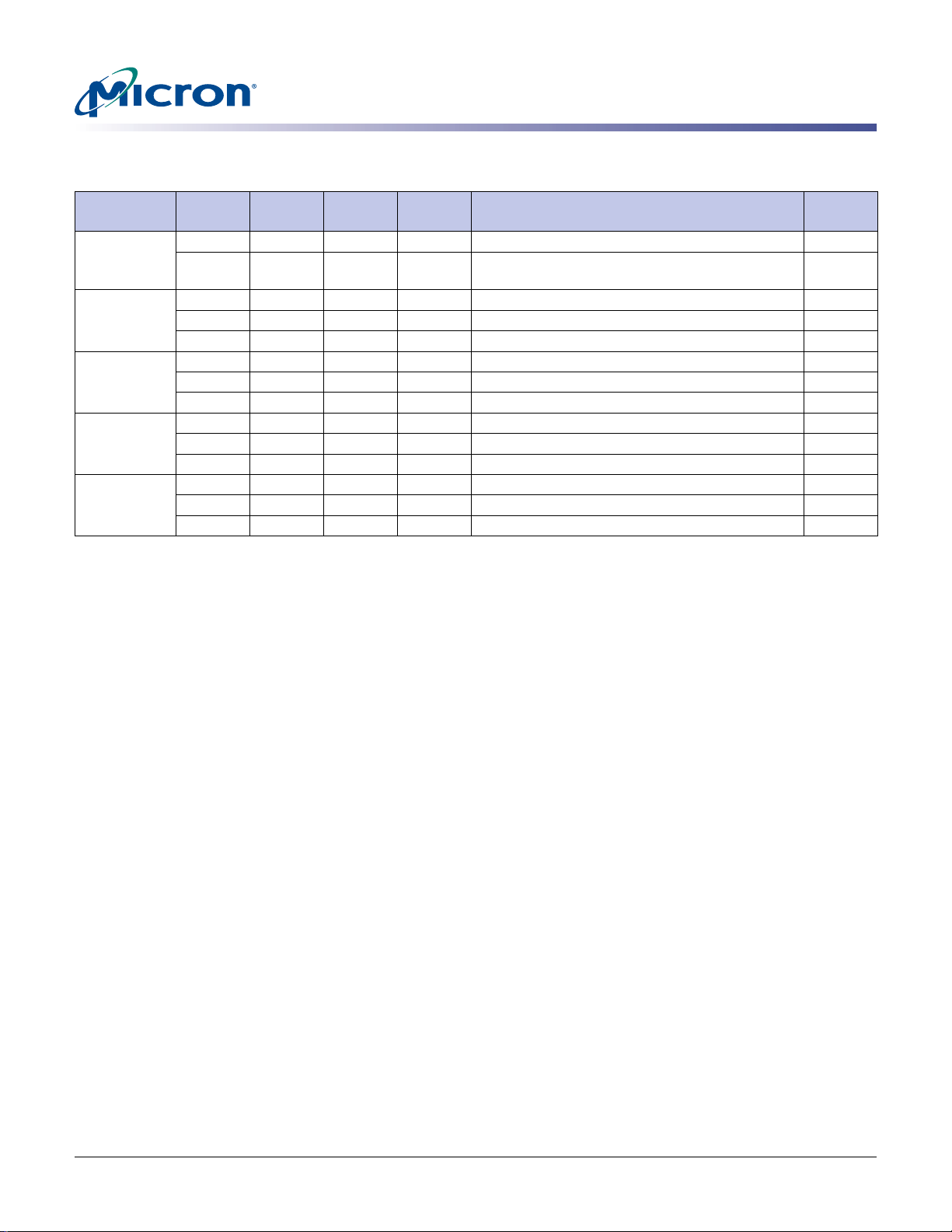
512Mb: x4, x8, x16 DDR2 SDRAM
Command Truth Tables
Table 6: Truth Table – Current State Bank n - Command to Bank n
Notes: 1–6; notes appear below and on next page
Current
State CS# RAS# CAS# WE# Command/Action Notes
Any
Idle
Row active
Read (autoprecharge
Disabled
Write (autoprecharge
disabled)
HXXX
LHHH
DESELECT (NOP/continue previous operati on)
NO OPERATION (NOP/continue previous
operation)
LLHH
LLLH
LLLL
LHLH
LHLL
LLHL
LHLH
LHLL
LLHL
LHLH
LHLL
LLHL
ACTIVE (select and activate row)
REFRESH
LOAD MODE
READ (select column and start READ burst)
WRITE (select column and start WRITE burst)
PRECHARGE (deactivate row in bank or banks)
READ (select column and start new READ burst)
WRITE (select column and start WRITE burst)
PRECHARGE (start PRECHARGE)
READ (select column and start READ burst)
WRITE (select column and start new WRITE burst)
PRECHARGE (start PRECHARGE)
7
7
9
9
8
9
9, 10
8
9
9
8
Notes: 1. This table applies when CKEn - 1 was HIGH and CKEn is HIGH and after tXSNR has been met
(if the previous state was self refresh).
2. This table is bank-specific, except where noted (the current state is for a specific bank and
the commands shown are those allowed to be issued to that bank when in that state).
Exceptions are covered in the notes below.
3. Current state definitions:
t
Idle: The bank has been precharged,
complete.
Row active: A row in the bank has been activated, and
RP has been met, and any READ burst is
t
RCD has been met. No data bursts/
accesses and no register accesses are in progress.
Read: A READ burst has been initiated, with auto precharge disabled, and has not
yet terminated.
Write: A WRITE burst has been initia ted, with auto precharge disabled, and has not
yet terminated.
4. The following states must not be interrupted by a command issued to the same bank. Issue
DESELECT or NOP commands, or allowable commands to the other bank, on any clock edge
occurring during these states. Allowable commands to the other bank are determined by its
current state and this table, and according to Table 7 on page 32.
Precharging: Starts with registration of a PRECHARGE command and ends when
is met. Once
Read with auto
precharge enabled:
Starts with registration of a READ command with auto precharge
enabled and ends when
will be in the idle state.
Row activating: Starts with registration of an ACTIVE command and ends when
t
RP is met, the bank will be in the idle state.
t
RP has been met. Once tRP is met, the bank
t
RCD is
met. Once tRCD is met, the bank will be in the “row active” state.
Write with auto
precharge enabled:
Starts with registration of a WRITE command with auto precharge
enabled and ends when
t
RP has been met. Once tRP is met, the bank
will be in the idle state.
t
RP
PDF: 09005aef8117c18e, Source: 09005aef8211b2e6 Micron Technology, Inc., reserves the right to change products or specifications without notice.
512MbDDR2_2.fm - R ev. K 8/06 EN
30 ©2004 Micron Technology, Inc. All rights reserved.
Page 31

512Mb: x4, x8, x16 DDR2 SDRAM
Command Truth Tables
5. The following states must not be interrupted by any executable command (DESELECT or
NOP commands must be applied on each positive clock edge during these states):
t
Refreshing: Starts with registration of a REFRESH command and ends when
met. Once
Accessing mode
register:
Starts with registration of the LM command and ends when tMRD has
been met. Once
t
RFC is met, the DDR2 SDRAM will be in the all banks idle state.
t
MRD is met, the DDR2 SDRAM will be in the all banks idle
state.
Precharging all: Starts with registration of a PRECHARGE ALL command and ends when
t
RP is met. Once tRP is met, all banks will be in the idle state.
6. All states and sequences not shown are illegal or reserved.
7. Not bank-specific; requires that all banks are idle and bursts are not in progress.
8. May or may not be bank-specific; if multiple banks are to be precharged, each must be in a
valid state for precharging.
9. READs or WRITEs listed in the Command/Action column include READs or WRITEs with auto
precharge enabled and READs or WRITEs with auto precharge disabled.
10. A WRITE command may be applied after the completion of the READ burst.
RFC is
PDF: 09005aef8117c18e, Source: 09005aef8211b2e6 Micron Technology, Inc., reserves the right to change products or specifications without notice.
512MbDDR2_2.fm - R ev. K 8/06 EN
31 ©2004 Micron Technology, Inc. All rights reserved.
Page 32
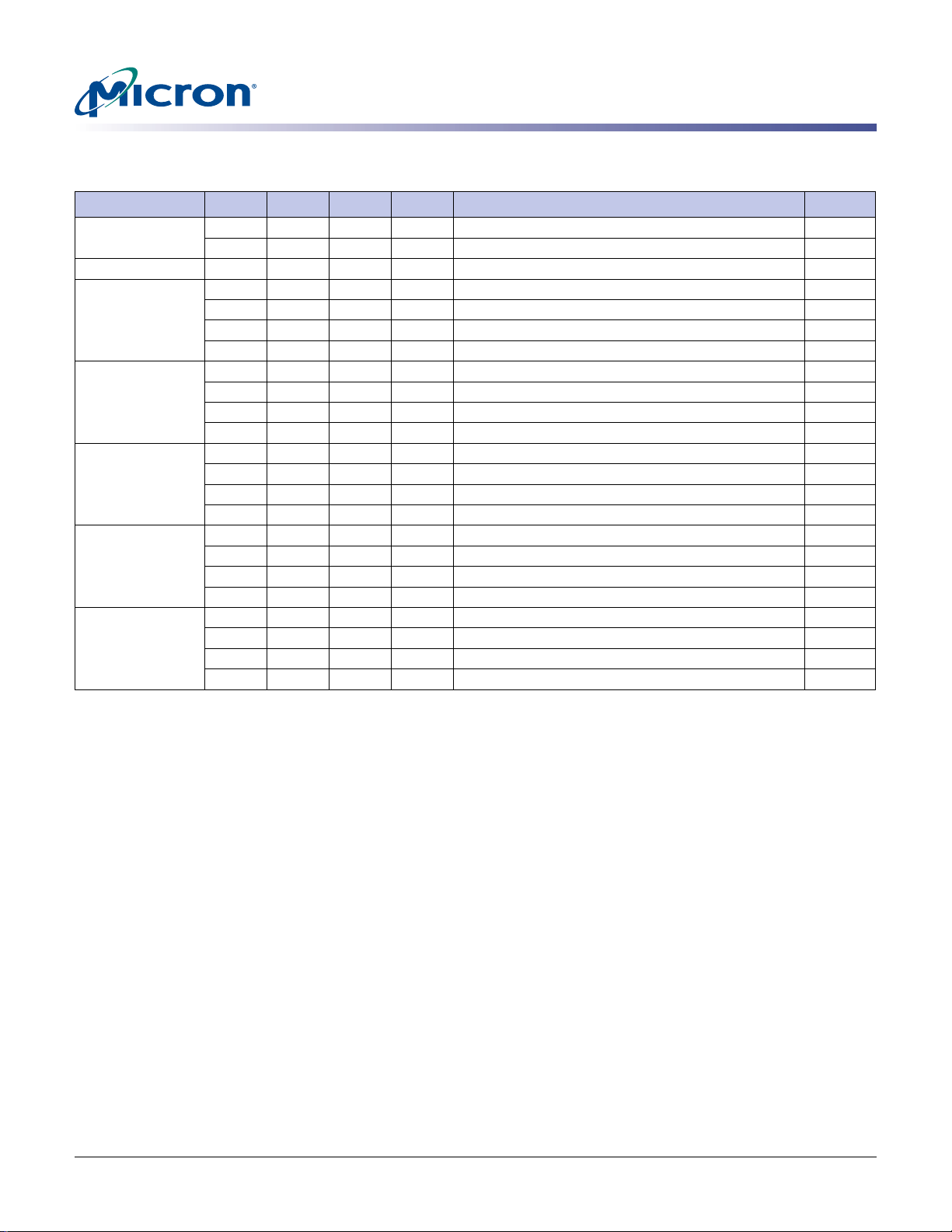
512Mb: x4, x8, x16 DDR2 SDRAM
Command Truth Tables
Table 7: Truth Table – Current State Bank n - Command to Bank m
Notes: 1–6; notes appear below and on next page
Current State CS# RAS# CAS# WE# Command/Action Notes
Any
Idle
Row Activating,
Active, or
Precharging
Read (auto
precharge
disabled
Write (auto
precharge
disabled.)
Read (with autoprecharge)
Write (with autoprecharge)
HXXX
LHHH
XXXX
LLHH
LHLH
LHLL
LLHL
LLHH
LHLH
LHLL
LLHL
LLHH
LHLH
LHLL
LLHL
LLHH
LHLH
LHLL
LLHL
LLHH
LHLH
LHLL
LLHL
Notes: 1. This table applies when CKEn - 1 was HIGH and CKEn is HIGH and after tXSNR has been met
(if the previous state was self refresh).
2. This table describes alternate bank operation, except where noted (i.e., the current state is
for bank n and the commands shown are those allowed to be issued to bank m, assuming
that bank m is in such a state that the given command is allowable). Exceptions are covered
in the notes below.
3. Current state definitions:
Idle: The bank has been precharged,
complete.
Row active: A row in the bank ha s been activated and
accesses and no register accesses are in progress.
Read: A READ burst has been initiated with auto precharge disabled, and has not
yet terminated.
Write: A WRITE burst has been initiated, with auto precharge disabled, and has not
yet terminated.
DESELECT (NOP/continue previous operation)
NO OPERATION (NOP/continue previous operation)
Any command otherwise allowed to bank m
ACTIVE (select and activate row)
READ (select column and start READ burst)
WRITE (select column and start WRITE burst)
PRECHARGE
ACTIVE (select and activate row)
READ (select column and start new READ burst)
WRITE (select column and start WRITE burst)
PRECHARGE
ACTIVE (select and activate row)
READ (select column and start READ burst)
WRITE (select column and start new WRITE burst)
PRECHARGE
ACTIVE (select and activate row)
READ (select column and start new READ burst)
WRITE (select column and start WRITE burst)
PRECHARGE
ACTIVE (select and activate row)
READ (select column and start READ burst)
WRITE (select column and start new WRITE burst)
PRECHARGE
t
RP has been met, and any READ burst is
t
RCD has been met. No data bursts/
7
7
7
7, 9
7, 8
7
7, 3
7, 9, 3
7, 3
7, 3
PDF: 09005aef8117c18e, Source: 09005aef8211b2e6 Micron Technology, Inc., reserves the right to change products or specifications without notice.
512MbDDR2_2.fm - R ev. K 8/06 EN
32 ©2004 Micron Technology, Inc. All rights reserved.
Page 33
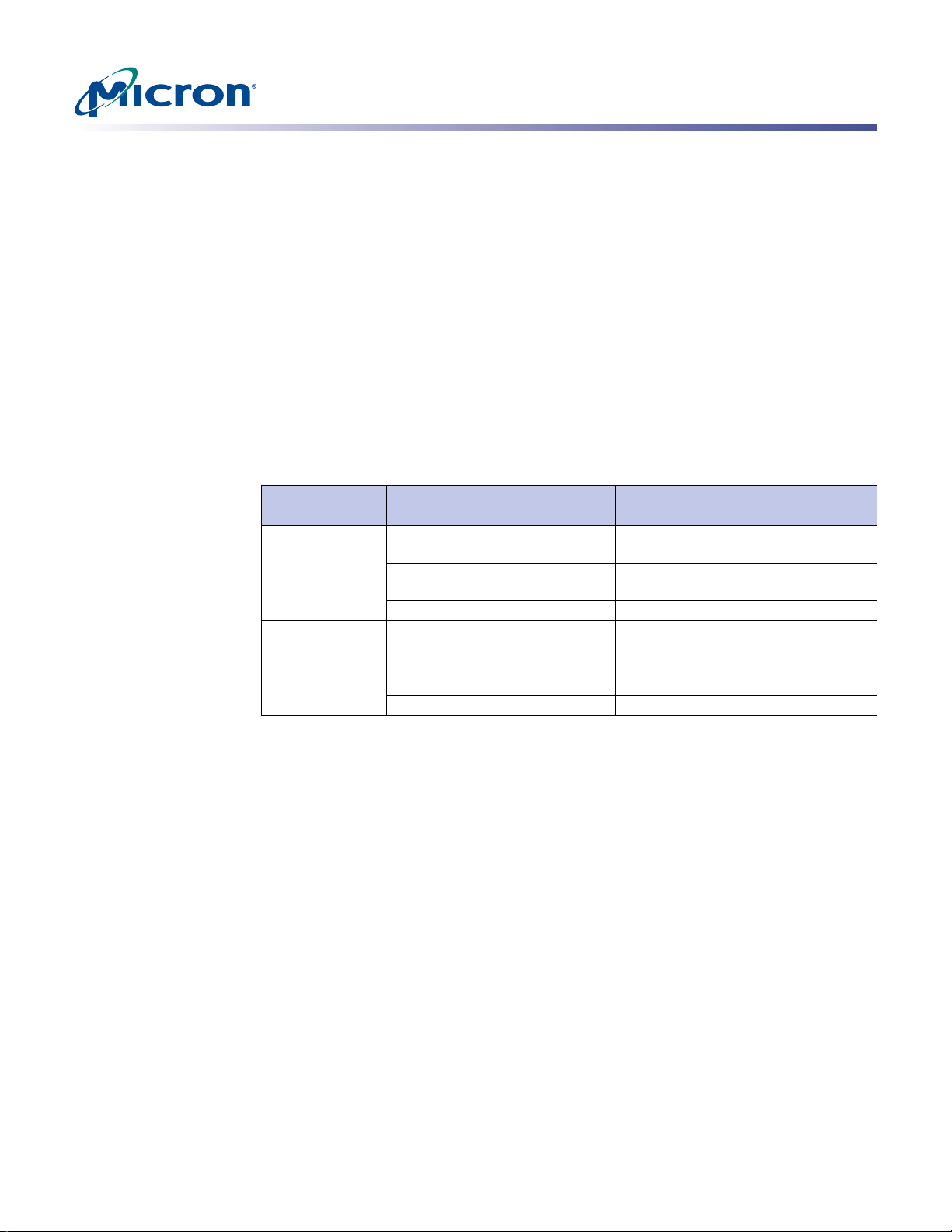
512Mb: x4, x8, x16 DDR2 SDRAM
Command Truth Tables
READ with
auto
precharge
enabled/
WRITE with
auto
precharge
enabled:
The READ with auto precharge enabled or WRITE with auto precharge
enabled states can each be broken into two parts: the access period and the
precharge period. For READ with auto precharge, the precharge period is
defined as if the same burst was executed with auto precharge disabled and
then followed with the earliest possible PRECHARGE command that still
accesses all of the data in the burst. For WRITE with auto precharge, the
precharge period begins when
precharge was disabled. The access period starts with registration of the
command and ends where the precharge period (or
supports concurrent auto precharge such that when a READ with auto
precharge is enabled or a WRITE with auto precharge is enabled, any
command to other banks is allowed, as long as that command does not
interrupt the read or write data transfer already in process. In either case, all
other related limitations apply (contention between read data and write data
must be avoided).
The minimum delay from a READ or WRITE command with auto prechar ge
enabled to a command to a different bank is summarized in Table 8:
Table 8: Minimum Delay with Auto Precharge Enabled
From Command
(Bank n)
WRITE with auto
precharge
READ with auto
precharge
To Command (Bank m)
READ or READ with auto
precharge
WRITE or WRITE with auto
precharge
PRECHARGE or ACTIVE 1
READ or READ with auto
precharge
WRITE or WRITE with auto
precharge
PRECHARGE or ACTIVE 1
t
WR ends, with tWR measured as if auto
t
RP) begins. This device
Minimum Delay (With
Concurrent Auto Precharge)
t
(CL - 1) + (BL / 2) +
WTR
(BL / 2)
(BL / 2)
(BL / 2) + 2
Units
t
CK
t
CK
t
CK
t
CK
t
CK
t
CK
4. REFRESH and LM commands may only be issued when all banks are idle.
5. Not used.
6. All states and sequences not shown are illegal or reserved.
7. READs or WRITEs listed in the Command/Action column include READs or WRITEs with auto
precharge enabled and READs or WRITEs with auto precharge disabled.
8. Requires appropriate DM.
9. A WRITE command may be applied after the completion of the READ burst.
t
10. The number of clock cycles required to meet
WTR is either 2 or tWTR/tCK, whichever is
greater.
PDF: 09005aef8117c18e, Source: 09005aef8211b2e6 Micron Technology, Inc., reserves the right to change products or specifications without notice.
512MbDDR2_2.fm - R ev. K 8/06 EN
33 ©2004 Micron Technology, Inc. All rights reserved.
Page 34

DESELECT, NOP, and LM Commands
DESELECT
The DESELECT function (CS# HIGH) prevents new commands from being executed by
the DDR2 SDRAM. The DDR2 SDRAM is effectively deselected. Operations already in
progress are not affected. DESEL ECT is also referred to as COMMAND INHIBIT.
NO OPERATION (NOP)
The NO OPERATION (NOP) command is used to instruct the selected DDR2 SD RAM to
perform a NOP (CS# is LOW; RAS#, CAS#, and WE are HIGH). This prevents unwanted
commands from being registered during idle or wait states. Operations already in
progress are not affected.
LOAD MODE (LM)
The mode registers are loaded via inputs BA1–BA0 and A13–A0 for x4 and x8, and A12–A0
for x16 configurations. BA1–BA0 determine which mode register will be programmed.
See “Mode Register (MR)” on page19. The LM command can only be issued when all
banks are idle, and a subsequent executable command cannot be issued until
met.
512Mb: x4, x8, x16 DDR2 SDRAM
DESELECT, NOP, and LM Commands
t
MRD is
Bank/Row Activation
ACTIVE Command
The ACTIVE command is used to open (or activate) a row in a particular bank for a
subsequent access. The value on the BA1–BA0 inputs selects the bank, and the address
provided on inputs (A13–A0 for x4 and x8, and A12–A0 for x16) selects the row. This row
remains active (or open) for accesses until a PRECHARGE command is issued to that
bank. A PRECHARGE command must be issued before opening a different row in the
same bank.
ACTIVE Operation
Before any READ or WRITE commands can be issued to a bank within the DDR2
SDRAM, a row in that bank must be opened (activated), even when additive latency is
used. This is accomplished via the ACTIVE command, which selects both the bank and
the row to be activated, as shown in Figure 15 on page 35.
After a row is opened with an ACTIVE command, a READ or WRITE command may be
issued to that row subject to the
the clock period and rounded up to the next whole number to determine the earliest
clock edge after the ACTIVE command on which a READ or WRITE command can be
entered. The same procedure is used to convert other specification limits from time
units to clock cycles. For example, a
clock (
page 37, which covers any case where 5 <
case for
t
RCD specification. tRCD (MIN) should be divided by
t
t
CK = 3.75ns) results in 5.3 clocks, rounded up to 6. This is reflected in Figure17 on
t
RRD where 2 < tRRD (MIN) / tCK ≤ 3.
RCD (MIN) specification of 20ns with a 266 MHz
t
RCD (MIN) / tCK ≤ 6. Figure 17 also shows the
A subsequent ACTIVE command to a different row in the same bank can only be issued
after the previous active row has been closed (precharged). The minimum time interval
between successive ACTIVE commands to the same bank is defined by
PDF: 09005aef8117c18e, Source: 09005aef8211b2e6 Micron Technology, Inc., reserves the right to change products or specifications without notice.
512MbDDR2_2.fm - R ev. K 8/06 EN
34 ©2004 Micron Technology, Inc. All rights reserved.
t
RC.
Page 35
A subsequent ACTIVE command to another bank can be issued while the first bank is
being accessed, which results i n a reduction of total ro w-acces s o verhead. The mini mum
time interval between successive ACTIVE commands to different banks is defined by
t
RRD.
Figure 15: ACTIVE Command
512Mb: x4, x8, x16 DDR2 SDRAM
Bank/Row Activation
CK#
CK
CKE
CS#
RAS#
CAS#
WE#
ADDRESS
BANK ADDRESS
Row
Bank
DON’T CARE
DDR2 SDRAM also supports the AL f eatur e, which allows a READ or WRITE command to
be issued prior to
t
RCD (MIN) by delaying the actual registration of the READ/WRITE
command to the internal device by AL clock cycles.
PDF: 09005aef8117c18e, Source: 09005aef8211b2e6 Micron Technology, Inc., reserves the right to change products or specifications without notice.
512MbDDR2_2.fm - R ev. K 8/06 EN
35 ©2004 Micron Technology, Inc. All rights reserved.
Page 36

READs
READ Command
READ Operation
512Mb: x4, x8, x16 DDR2 SDRAM
READs
The READ command is used to initiate a burst re ad access to an active row. The value on
the BA1–BA0 inputs selects the bank, and the address provided on inputs A 0–i (wher e i =
A9 for x16, A9 for x8, or A9, A11 for x4) selects the starting column location. The value on
input A10 determines whether or not auto precharge is used. If auto precharge is
selected, the row being accessed will be pr e char ged at the end of the READ burst; if auto
precharge is not selected, the row will remain open for subsequent accesses.
READ bursts are initiated with a READ command, as shown in Figure 16 on page 37. The
starting column and bank addresses are provided with the READ command and auto
precharge is either enabled or disabled for that burst access. If auto precharge is
enabled, the row being accesse d is automatically precharged at the completion of the
burst. If auto precharge is disabled, the row will be left open after the completion of the
burst.
During READ bursts, the valid data-out element from the starting column address will
be available READ latency (RL) clocks later. RL is defined as the sum of AL and CL;
RL = AL + CL. The value for AL and CL are programmable via the MR and EMR
commands, respectively. Each subsequent data-out element will be valid nominally at
the next positive or negative clock edge (i.e., at the next crossing of CK and CK#).
Figure18 on page 38 shows examples of RL based on different AL and CL settings.
DQS/DQS# is driven by the DDR2 SDRAM along with output data. The initial LOW state
on DQS and HIGH state on DQS# is known as the read preamble (
on DQS and HIGH state on DQS# coincident with the last data-out element is known as
the read postamble (
Upon completion of a burst, assuming no other commands have been initiated, the DQ
will go High-Z. A detailed explanation of
t
RPST).
t
DQSQ (valid data-out skew), tQH (data-out
t
RPRE). The LOW state
window hold), and the valid data window are depicted in Figure27 on page 46 and
Figure28 on page 47. A detailed explanation of
t
AC (data-out transition skew to CK) is shown in Figure 29 on page 48.
t
DQSCK (DQS transition skew to CK) and
Data from any READ burst may be concatenated with data from a subsequent READ
command to provide a continuous flow of data. The first data element from the new
burst follows the last element of a completed burst. The new READ command should be
issued x cycles after the first READ command, where x equals BL / 2 cycles. This is sho wn
in Figure19 on page 39.
PDF: 09005aef8117c18e, Source: 09005aef8211b2e6 Micron Technology, Inc., reserves the right to change products or specifications without notice.
512MbDDR2_2.fm - R ev. K 8/06 EN
36 ©2004 Micron Technology, Inc. All rights reserved.
Page 37
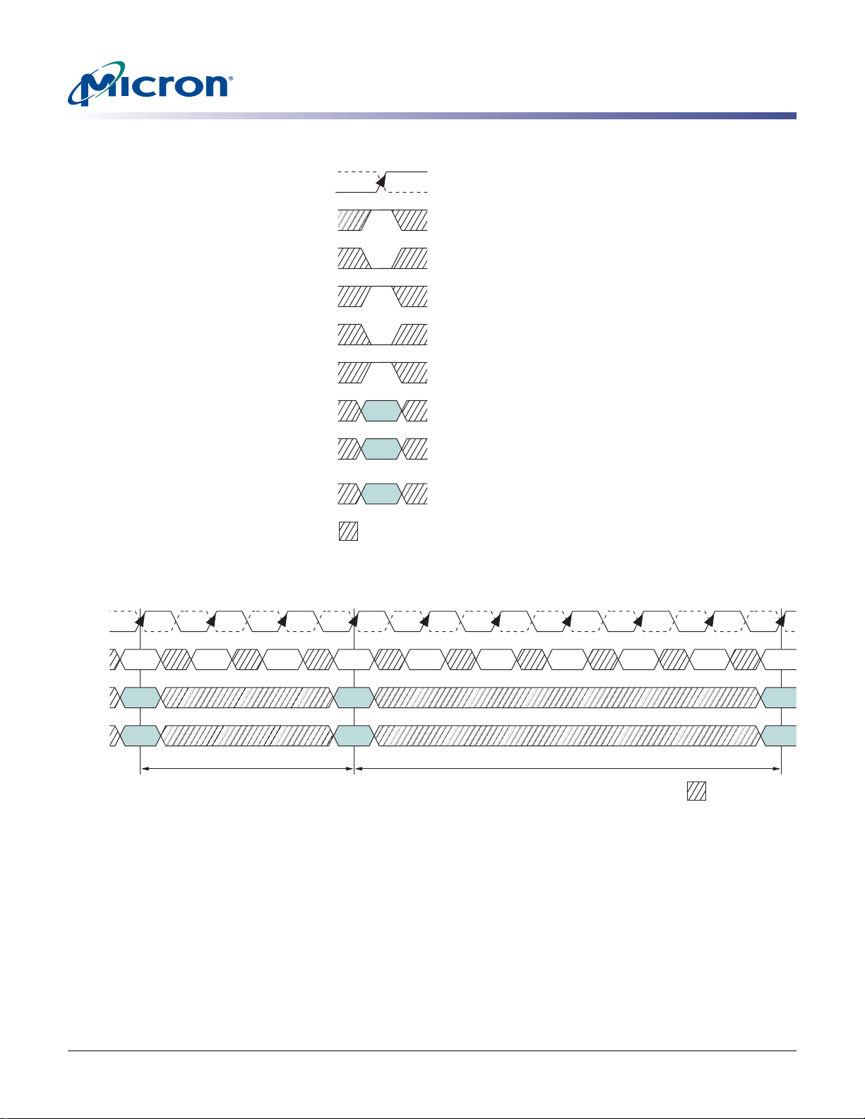
Figure 16: READ Command
512Mb: x4, x8, x16 DDR2 SDRAM
READs
CK#
CK
CKE
CS#
RAS#
CAS#
WE#
ADDRESS
AUTO PRECHARGE
BANK ADDRESS
Figure 17: Example: Meeting
CK#
CK
AND
RESS
, BA1
Row Row
Bank x Bank y
T1T0 T2 T3 T4 T5 T6 T7
NOPACT NOP NOPACT NOP NOP RD/WR
t
RRD
Col
ENABLE
A10
DISABLE
Bank
DON’T CARE
t
RRD (MIN) and tRCD (MIN)
t
RCD
NOP
T8
NOP
DON’T CARE
T9
Col
Bank y
PDF: 09005aef8117c18e, Source: 09005aef8211b2e6 Micron Technology, Inc., reserves the right to change products or specifications without notice.
512MbDDR2_2.fm - R ev. K 8/06 EN
37 ©2004 Micron Technology, Inc. All rights reserved.
Page 38
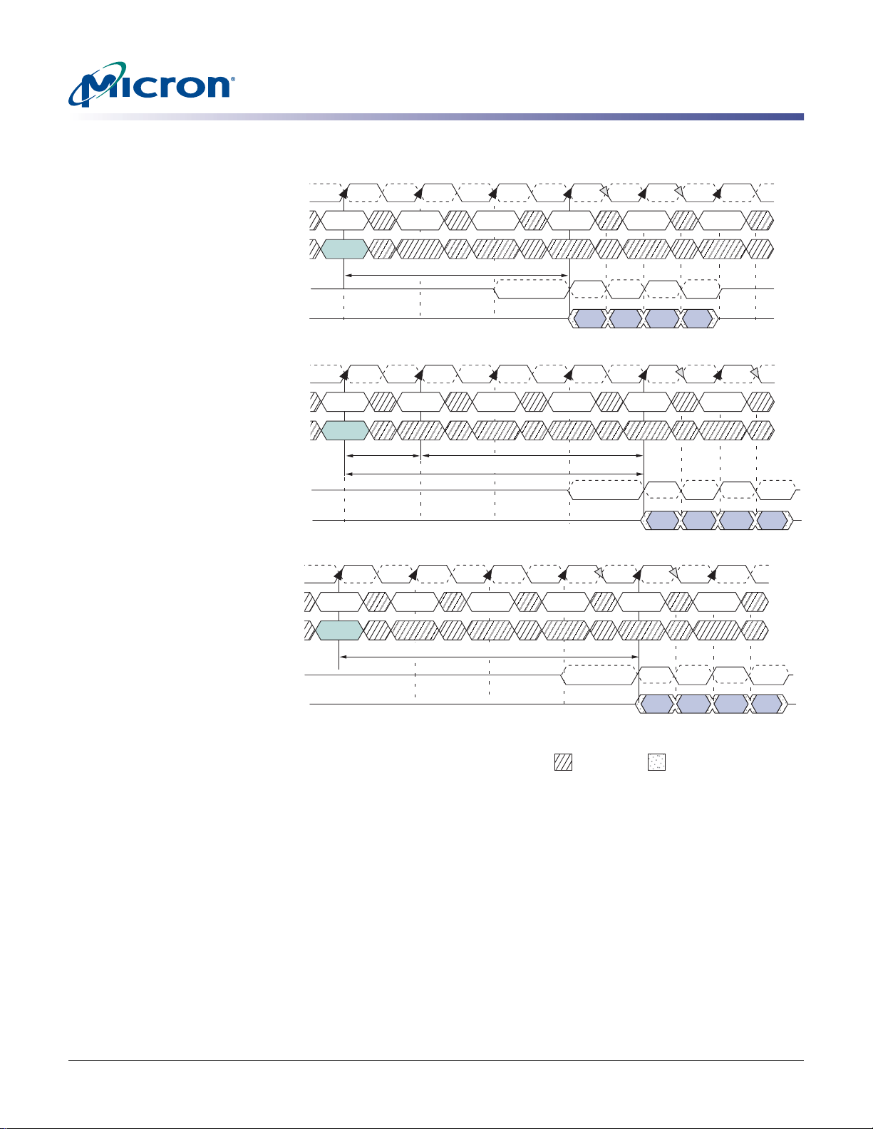
Figure 18: READ Latency
512Mb: x4, x8, x16 DDR2 SDRAM
READs
CK#
CK
COMMAND
ADDRESS
DQS, DQS#
DQ
CK#
COMMAND
ADDRESS
DQS, DQS#
DQ
CK#
CK
COMMAND
ADDRESS
DQS, DQS#
T0 T1 T2 T3 T3n T4nT4 T5
READ NOP NOP NOP NOP NOP
Bank a,
Col n
T0 T1 T2 T3 T4n T5nT4 T5
CK
READ NOP NOP NOP NOP NOP
Bank a,
Col n
T0 T1 T2 T3 T3n T4nT4 T5
READ NOP NOP NOP NOP NOP
Bank a,
Col n
RL = 3 (AL = 0, CL = 3)
AL = 1
CL = 3
RL = 4 (AL = 1 + CL = 3)
RL = 4 (AL = 0, CL = 4)
DO
n
DO
n
DQ
DON’T CARE
DO
n
TRANSITIONING DATA
Notes: 1. DO n = data-out from column n.
2. BL = 4.
3. Three subsequent elements of data-out appear in the programmed order following DO n.
t
4. Shown with nominal
PDF: 09005aef8117c18e, Source: 09005aef8211b2e6 Micron Technology, Inc., reserves the right to change products or specifications without notice.
512MbDDR2_2.fm - R ev. K 8/06 EN
AC, tDQSCK, and tDQSQ.
38 ©2004 Micron Technology, Inc. All rights reserved.
Page 39
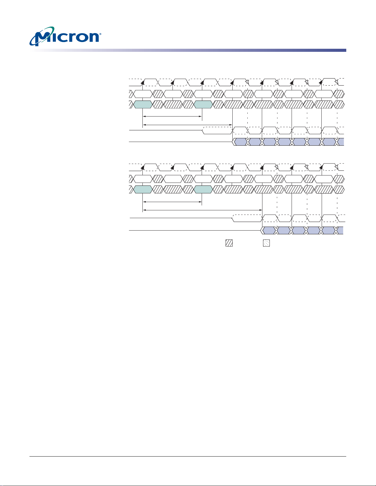
Figure 19: Consecutive READ Bursts
512Mb: x4, x8, x16 DDR2 SDRAM
READs
CK#
CK
COMMAND
ADDRESS
DQS, DQS#
DQ
CK#
CK
COMMAND
COMMAND
ADDRESS
ADDRESS
DQS, DQS#
DQ
T0 T1 T2 T3 T3n T4nT4 T5 T6
READ NOP READ NOP NOP NOP NOP
Bank,
Col n
T0 T1 T2 T3T2n
READ NOP READ NOP NOP NOP
Bank,
Col n
t
CCD
RL = 3
t
CCD
RL = 4
Bank,
Col b
Bank,
Col b
DO
n
T3n T4nT4 T5 T6
DO
n
DON’T CARE TRANSITIONING DATA
T5n T6n
DO
b
T5n T6n
NOP
DO
b
Notes: 1. DO n (or b) = data-out from column n (or column b).
2. BL = 4.
3. Three subsequent elements of data-out appear in the programmed order following DO n.
4. Three subsequent elements of data-out appear in the programmed order following DO b.
t
5. Shown with nominal
AC, tDQSCK, and tDQSQ.
6. Example applies only when READ commands are issued to same device.
Nonconsecutive read data is illustrated in Figure 20 on page 40. Full-speed random read
accesses within a page (or pages) can be performed. DDR2 SDRAM supports the use of
concurrent auto precharge timing, shown in Table 9 on page 41.
DDR2 SDRAM does not allow interrupting or truncating of any READ burst using BL = 4
operations. Once the BL = 4 READ command is registered, it must be allowed to
complete the entire READ burst. However, a READ (with auto precharge disabled) using
BL = 8 operation may be interrupted and truncated only by another READ burst as long
as the interruption occurs on a 4-bit boundary due to the 4n prefetch architecture of
DDR2 SDRAM. READ burst BL = 8 operations may not be interrupted or truncated with
any command except another READ command, as shown in Figure21 on page 40.
PDF: 09005aef8117c18e, Source: 09005aef8211b2e6 Micron Technology, Inc., reserves the right to change products or specifications without notice.
512MbDDR2_2.fm - R ev. K 8/06 EN
39 ©2004 Micron Technology, Inc. All rights reserved.
Page 40
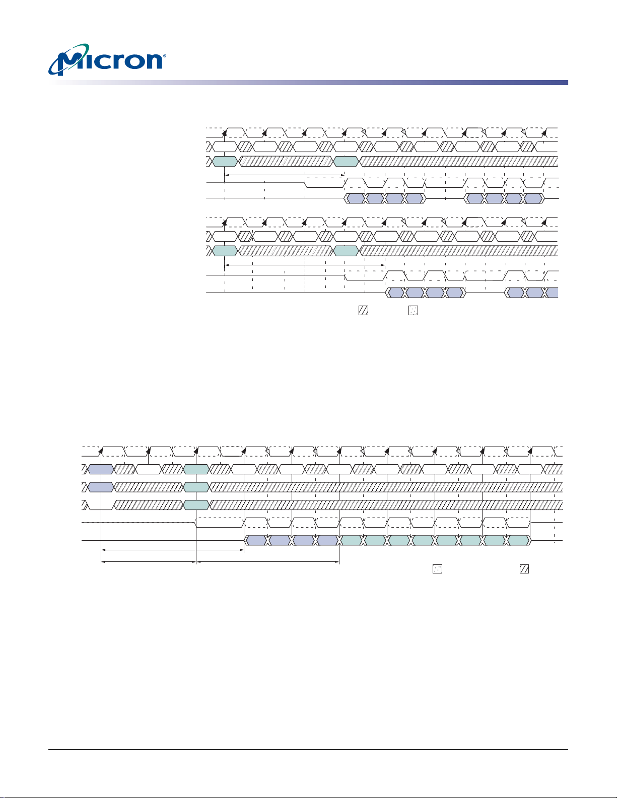
Figure 20: Nonconsecutive READ Bursts
512Mb: x4, x8, x16 DDR2 SDRAM
READs
CK#
COMMAND
ADDRESS
DQS, DQS#
DQ
CK#
COMMAND
COMMAND
ADDRESS
ADDRESS
DQS, DQS#
DQ
T0 T1 T2 T3 T3n T4 T5 T7 T8T6T4n T6n T7n
CK
READ NOP NOP NOP NOP NOP NOP NOP
Bank,
Col n
T0 T1 T2 T3 T4
CK
READ NOP NOP NOP
Bank,
Col n
CL = 3
CL = 4
READ
Bank,
Col b
READ
Bank,
Col b
DO
n
DO
n
DON’T CARE TRANSITIONING DATA
Notes: 1. DO n (or b) = data-out from column n (or column b).
2. BL = 4.
3. Three subsequent elements of data-out appear in the programmed order following DO n.
4. Three subsequent elements of data-out appear in the programmed order following DO b.
5. Shown with nominal tAC, tDQSCK, and tDQSQ.
6. Example applies when READ commands are issued to different devices or nonconsecutive
READs.
DO
b
T5 T7 T8T5n T6T4n T7n
NOP NOP NOP NOP
DO
b
Figure 21: READ Interrupted by READ
CK#
CK
COMMAND
ADDRESS
A10
DQS, DQS#
DQ
T0 T1 T2
5
READ
VALID
1
2
NOP
CL = 3 (AL = 0)
t
CCD
Notes: 1. BL = 8 required; auto precharge must be disabled (A10 = LOW).
2. READ command can be issued to any valid bank and row address (READ command at T0 and
3. Interrupting READ command must be issued exactly 2 x tCK from previous READ.
4. Auto precharge can be either enabled (A10 = HIGH) or disabled (A10 = LOW) by the in ter-
5. NOP or COMMAND INHIBIT commands are valid. PRECHARGE command cannot be issued to
6. Example shown uses AL = 0; CL = 3, BL = 8, shown with nominal
3
READ
2
VALID
4
VALID
T2 can be either same bank or different bank).
rupting READ command.
banks used for READs at T0 and T2.
T3 T4 T5
NOP
5
D
CL = 3 (AL = 0)
VALID VALID
D
OUT
OUTDOUTDOUTDOUTDOUT
T6
VALID
D
OUTDOUTDOUT
T7 T8 T9
VALID VALID VALID
D
OUTDOUTDOUT
t
AC, tDQSCK, and tDQSQ.
DON’T CARETRANSITIONING DATA
PDF: 09005aef8117c18e, Source: 09005aef8211b2e6 Micron Technology, Inc., reserves the right to change products or specifications without notice.
512MbDDR2_2.fm - R ev. K 8/06 EN
40 ©2004 Micron Technology, Inc. All rights reserved.
Page 41
Table 9: READ Using Concurrent Auto Precharge
From
Command
(Bank n)
READ with
auto
precharge
READ or READ with auto precharge BL/2
WRITE or WRITE with auto precharge (BL/2) + 2
To Command
(Bank m)
PRECHARGE or ACTIVE 1
Data from any READ burst must be completed before a subsequent WRITE burst is
allowed. An example of a READ burst followed by a WRITE burst is shown in Figure 24 on
page 43. The
time. (
t
t
DQSS (MIN) case is shown; the tDQSS (MAX) case has a longer bus idle
DQSS [MIN] and tDQSS [MAX] are defined in Figure31 on page 51.)
A READ burst may be followed by a PRECHARGE command to the same bank, provided
that auto precharge was not activated. The minimum READ-to-PRECHARGE command
spacing to the same bank is AL + BL/2 clocks and must also satisfy a minimum analog
time from the rising clock edge that initiates the last 4-bit prefetch of a READ-toPRECHARGE command. This READ-to-PRECHARGE time is called
is the time from the actual READ (AL after the READ command) to PRECHARGE
command. For BL = 8 this is the time from AL + 2CK after the READ-to-PRECHARGE
command. Following the PRECHARGE command, a subsequent command to the same
bank cannot be issued until
t
RP is met.
Note: Part of the row precharge time is hidden during the access of the last data elements.
512Mb: x4, x8, x16 DDR2 SDRAM
Minimum Delay (with
Concurrent Auto Precharge)
t
RTP. For BL = 4 this
Units
t
t
t
READs
CK
CK
CK
Examples of READ-to-PRECHARGE are shown in Figure22 on page 42 for BL = 4 and
Figure23 on page 42 for BL = 8. The delay from READ-to-PRECHARGE command to the
same bank is AL + BL/2 + MAX (
t
RTP/tCK or 2CK) - 2CK.
If A10 is HIGH when a READ command is issued, the READ with auto precharge function
is engaged. The DDR2 SDRAM starts an auto precharge operation on the rising edge,
which is AL + (BL/2) cycles later than the READ with auto precharge command if
(MIN) and
auto precharge operation will be delayed until
t
RTP are satisfie d. If tRAS (MIN) is not satisfied at the edge, the start point of
t
RAS (MIN) is satisfied. If tRTP (MIN) is
t
RAS
not satisfied at the edge, the start point of the auto precharge operation will be delayed
t
until
RTP (MIN) is satisfied. In case the internal precharge is pushed out by tRTP, tRP
starts at the point where the internal precharge happens (not at the next rising clock
edge after this event). For BL = 4, the minimum time from READ with auto precharge to
the next ACTIVATE command becomes AL + (
t
RTP + tRP)*, shown in Figure22 on
page 42; for BL = 8, the time from READ with auto precharge to the next ACTIVATE
command is AL + 2 clocks + (
each parameter term is divided by
t
RTP + tRP)*, shown in Figure23 on page 42. The * indicates
t
CK and rounded up to the next integer. In any event,
internal precharge does not start earlier than two clocks after the last 4-bit prefetch.
PDF: 09005aef8117c18e, Source: 09005aef8211b2e6 Micron Technology, Inc., reserves the right to change products or specifications without notice.
512MbDDR2_2.fm - R ev. K 8/06 EN
41 ©2004 Micron Technology, Inc. All rights reserved.
Page 42
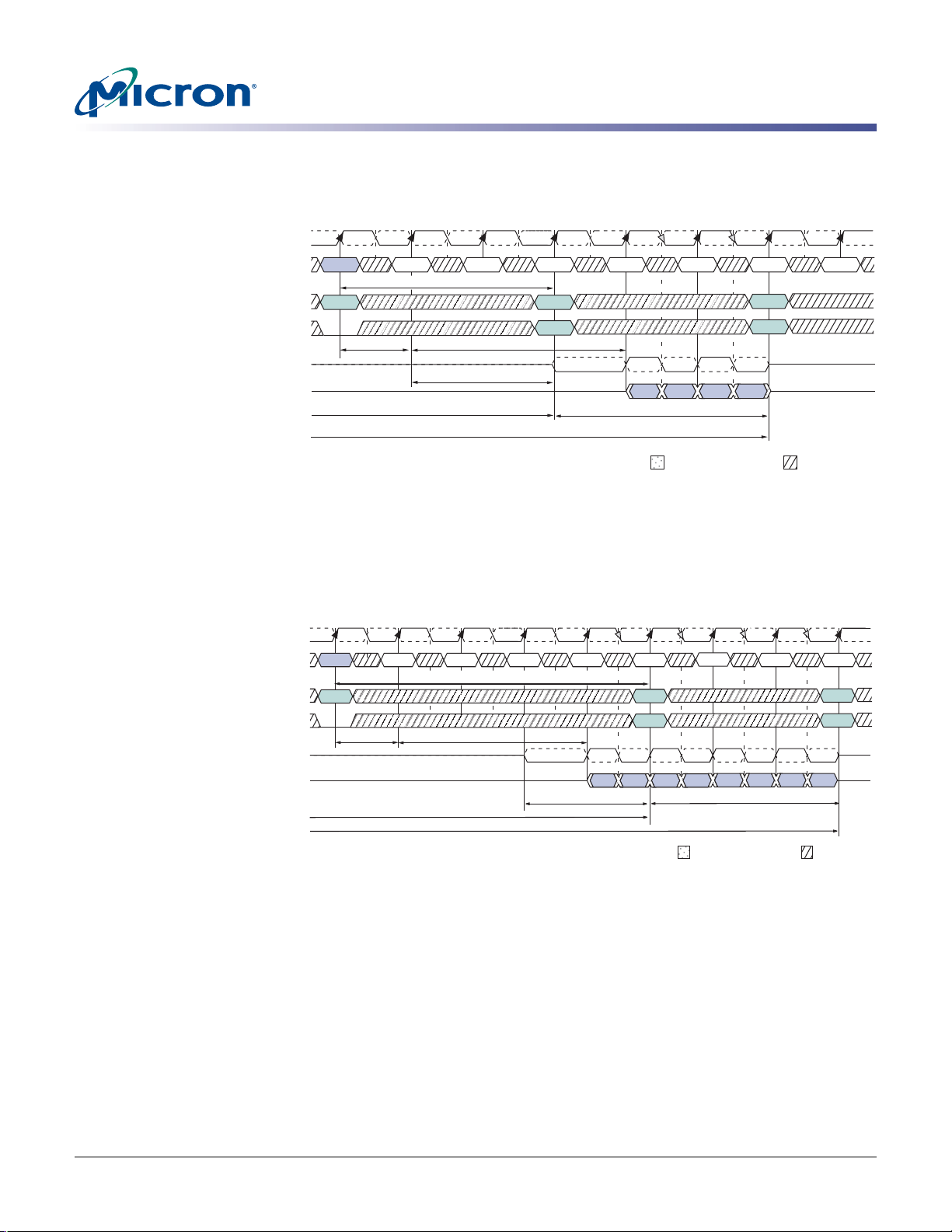
Figure 22: READ-to-PRECHARGE – BL = 4
T0 T1 T2
CK#
CK
COMMAND
ADDRESS
DQS, DQS#
READ
AL + BL/2 + MAX(tRTP/tCK or 2CK) - 2CK
Bank a
A10
AL = 1
DQ
4-bit
prefetch
NOP
≥
t
≥
RAS (MIN)
NOP
t
RTP (MIN)
512Mb: x4, x8, x16 DDR2 SDRAM
T3 T4 T5 T6
CL = 3
PRECHG
Bank a
Valid
t
≥
RC (MIN)
NOP NOP
D
OUT
D
OUTDOUTDOUT
t
≥
RP (MIN)
ACTIVE
Bank a
Valid
READs
T7
NOP
DON’T CARETRANSITIONING DATA
Notes: 1. RL = 4 (AL = 1, CL = 3); BL = 4.
t
2.
RTP ≥ 2 clocks.
3. Shown with nominal tAC, tDQSCK, and tDQSQ.
Figure 23: READ-to-PRECHARGE – BL = 8
first 4-bit
T0 T1 T2
CK#
CK
COMMAND
ADDRESS
DQS, DQS#
READ
Bank a
A10
DQ
Notes: 1. RL = 4 (AL = 1, CL = 3); BL = 8.
t
RTP ≥ 2 clocks.
2.
3. Shown with nominal
prefetch
NOP
AL = 1
second 4-bit
prefetch
T3 T4 T5 T6 T7 T8
NOP
AL + BL/2 + MAX(tRTP/tCK or 2CK) -2CK
CL = 3
≥tRAS (MIN)
t
AC, tDQSCK, and tDQSQ.
NOP
≥tRTP (MIN)
≥tRC (MIN)
NOP
PRECHG
Bank a
Valid
DOUT
DOUT DOUT DOUT DOUT DOUT DOUT DOUT
NOP
≥tRP (MIN)
NOP
ACTIVE
Bank a
Valid
DON’T CARETRANSITIONING DATA
PDF: 09005aef8117c18e, Source: 09005aef8211b2e6 Micron Technology, Inc., reserves the right to change products or specifications without notice.
512MbDDR2_2.fm - R ev. K 8/06 EN
42 ©2004 Micron Technology, Inc. All rights reserved.
Page 43
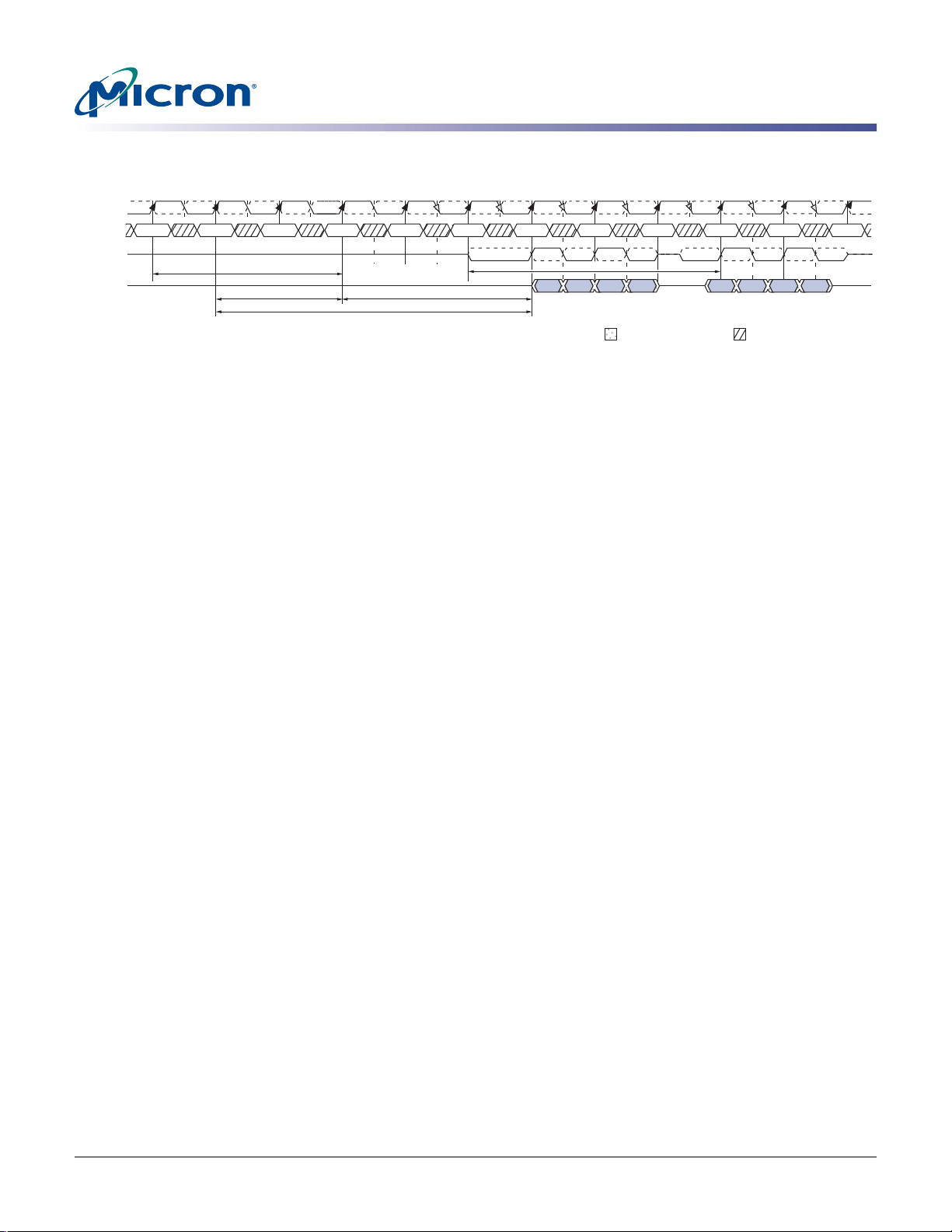
Figure 24: READ-to-WRITE
512Mb: x4, x8, x16 DDR2 SDRAM
READs
CK#
CK
COMMAND
DQS, DQS#
DQ
T0 T1 T2
ACTIVE n
READ n
t
RCD = 3
Notes: 1. BL = 4; CL = 3; AL = 2.
T3 T4 T5
NOP
AL = 2
NOP
NOP NOP
NOP WRITE n
RL = 5
2. Shown with nominal
T6
WRITE
CL = 3
t
AC, tDQSCK, and tDQSQ.
NOP
NOP
D
OUT
n
T7 T8
NOP NOP NOP
WL = RL - 1 = 4
D
OUT
n + 2
D
OUT
n + 3
D
OUT
n + 1
T9 T10 T11
NOP NOP
IN
D
D
IN
n + 1
n
DON’T CARETRANSITIONING DATA
D
n + 2
IN
D
IN
n + 3
PDF: 09005aef8117c18e, Source: 09005aef8211b2e6 Micron Technology, Inc., reserves the right to change products or specifications without notice.
512MbDDR2_2.fm - R ev. K 8/06 EN
43 ©2004 Micron Technology, Inc. All rights reserved.
Page 44
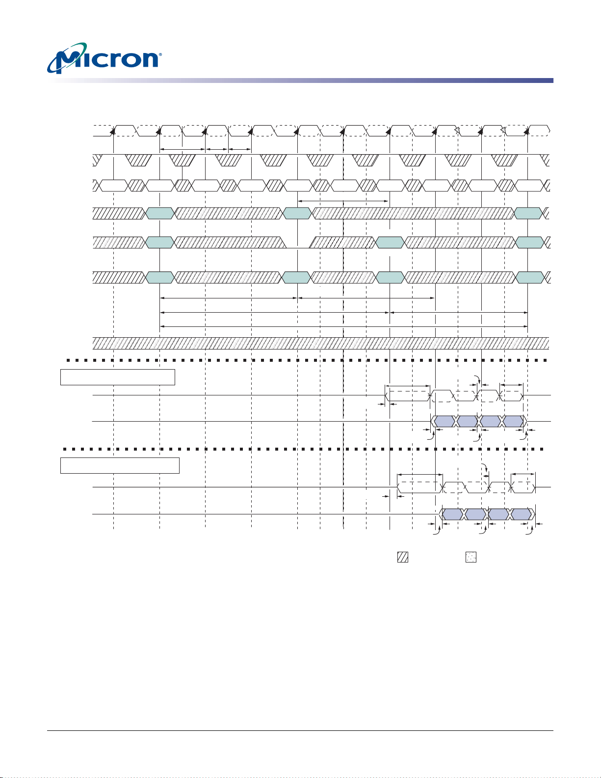
Figure 25: Bank Read – Without Auto Precharge
512Mb: x4, x8, x16 DDR2 SDRAM
READs
CK#
CK
CKE
COMMAND
ADDRESS
A10
BA0, BA1
DM
Case 1: tAC (MIN)
DQS, DQS#
DQ
T0
5
1
6
NOP
and tDQSCK (MIN)
T1
t
CK
ACT
RA Col n
RA
Bank x
T2 T3 T4 T5 T7n T8nT6 T7 T8
t
CHtCL
t
RCD
t
RAS
t
RC
NOP
7
6
NOP
6
READ
3
Bank x
2
CL = 3
NOP
t
RTP
6
8
t
LZ (MIN)
7
PRE
ALL BANKS
ONE BANK
4
t
RPRE
99
t
LZ (MIN)
6
NOP
t
RP
t
DQSCK (MIN)
DO
n
t
AC (MIN)
NOP
6
t
HZ (MIN)
t
RPST
ACT
RA
RA
Bank xBank x
Case 2: tAC (MAX) and tDQSCK (MAX)
DQS, DQS#
1
DQ
t
LZ (MAX)
9
t
t
LZ (MIN)
DON’T CARE
RPRE
DQSCK (MAX)
DO
n
t
AC (MAX)
t
RPST
9
t
HZ (MAX)
TRANSITIONING DATA
t
Notes: 1. DO n = data-out from column n; subsequent elements are applied in the programmed
order .
2. BL = 4 and AL = 0 in the case shown.
3. Disable auto precharge.
4. “Don’t Care” if A10 is HIGH at T5.
5. PRE = PRECHARGE, ACT = ACTIVE, RA = row address, BA = bank address.
6. NOP commands are shown for ease of illustration; other commands may be valid at these
times.
t
7. The PRECHARGE command can only be applied at T6 if
t
8. READ-to-PRECHARGE = AL + BL/2 + (
RTP - 2 clocks).
RAS (MIN) is met.
9. I/0 balls, when entering or exiting HIGH-Z are not referenced to a specific voltage level, but
to when the device begins to drive or no longer drives, respectively.
PDF: 09005aef8117c18e, Source: 09005aef8211b2e6 Micron Technology, Inc., reserves the right to change products or specifications without notice.
512MbDDR2_2.fm - R ev. K 8/06 EN
44 ©2004 Micron Technology, Inc. All rights reserved.
Page 45
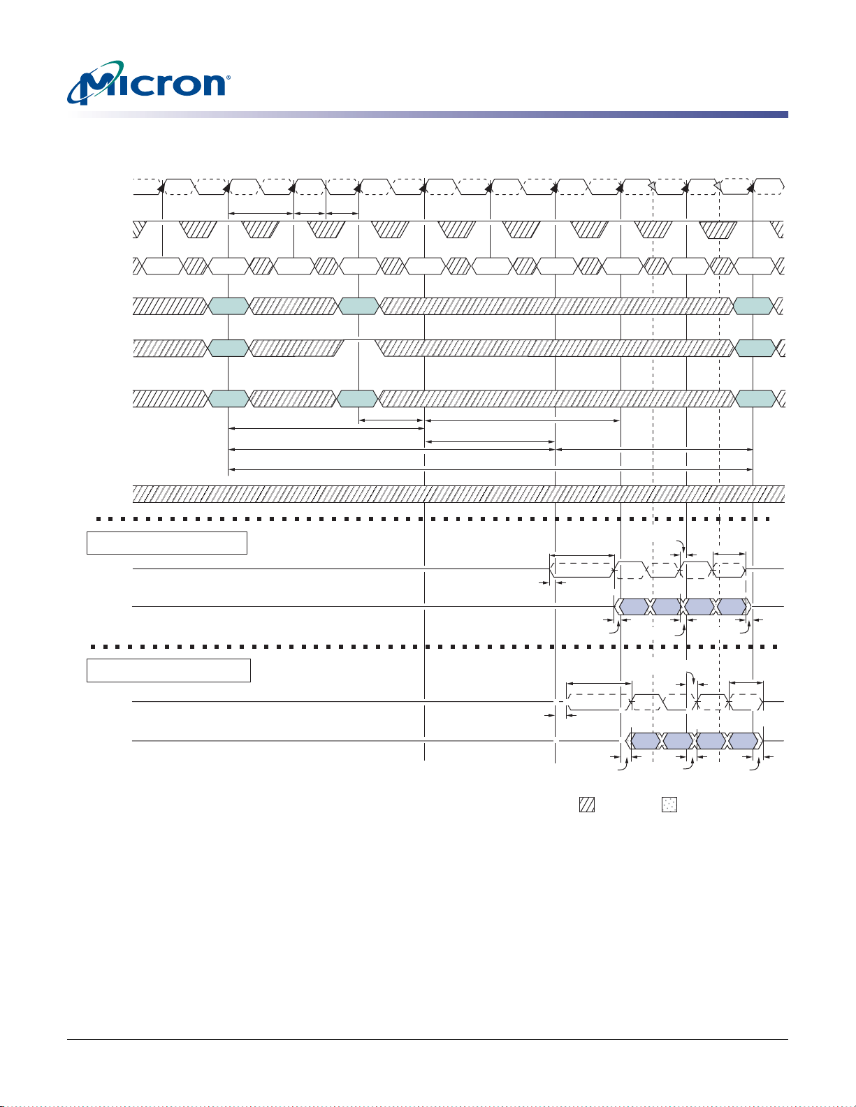
Figure 26: Bank Read – With Auto Precharge
512Mb: x4, x8, x16 DDR2 SDRAM
READs
CK#
CK
CKE
COMMAND
ADDRESS
A10
BA0, BA1
DM
Case 1: tAC (MIN)
DQS, DQS#
DQ
T0
5
1
5
NOP
and tDQSCK (MIN)
T1
ACT
RA
RA
Bank x
T2 T3 T4 T5 T7n T8nT6 T7 T8
t
CK
t
t
RCD
RAS
t
RC
NOP
tCHt
5
CL
READ
Col n
3
Bank x
2,6
AL = 1
NOP
5
t
NOP
RTP
5
CL = 3
t
LZ (MIN)
5
NOP
t
RPRE
77
t
LZ (MIN)
5
NOP
t
RP
t
DQSCK (MIN)
DO
n
t
AC (MIN)
NOP
5
t
t
HZ (MIN)
ACT
RA
RA
Bank x
RPST
Case 2: tAC (MAX) and tDQSCK (MAX)
DQS, DQS#
1
DQ
t
LZ (MAX)
4-bit
prefetch
7
Internal
precharge
t
LZ (MAX)
t
RPRE
DON’T CARE
DQSCK (MAX)
DO
n
t
AC (MAX)
t
RPST
7
t
HZ (MAX)
TRANSITIONING DATA
t
Notes: 1. DO n = data-out from column n; subsequent elements are applied in the programmed
order .
2. BL = 4, RL = 4 (AL = 1, CL = 3) in the case shown.
3. Enable auto precharge.
4. ACT = ACTIVE, RA = row address, BA = bank address.
5. NOP commands are shown for ease of illustration; other commands may be valid at these
times.
t
6. The DDR2 SDRAM internally delays auto precharge until both
RAS (MIN) and tRTP (MIN)
have been satisfied.
7. I/0 balls, when entering or exiting HIGH-Z are not referenced to a specific voltage level, but
to when the device begins to drive or no longer drives, respectively.
PDF: 09005aef8117c18e, Source: 09005aef8211b2e6 Micron Technology, Inc., reserves the right to change products or specifications without notice.
512MbDDR2_2.fm - R ev. K 8/06 EN
45 ©2004 Micron Technology, Inc. All rights reserved.
Page 46
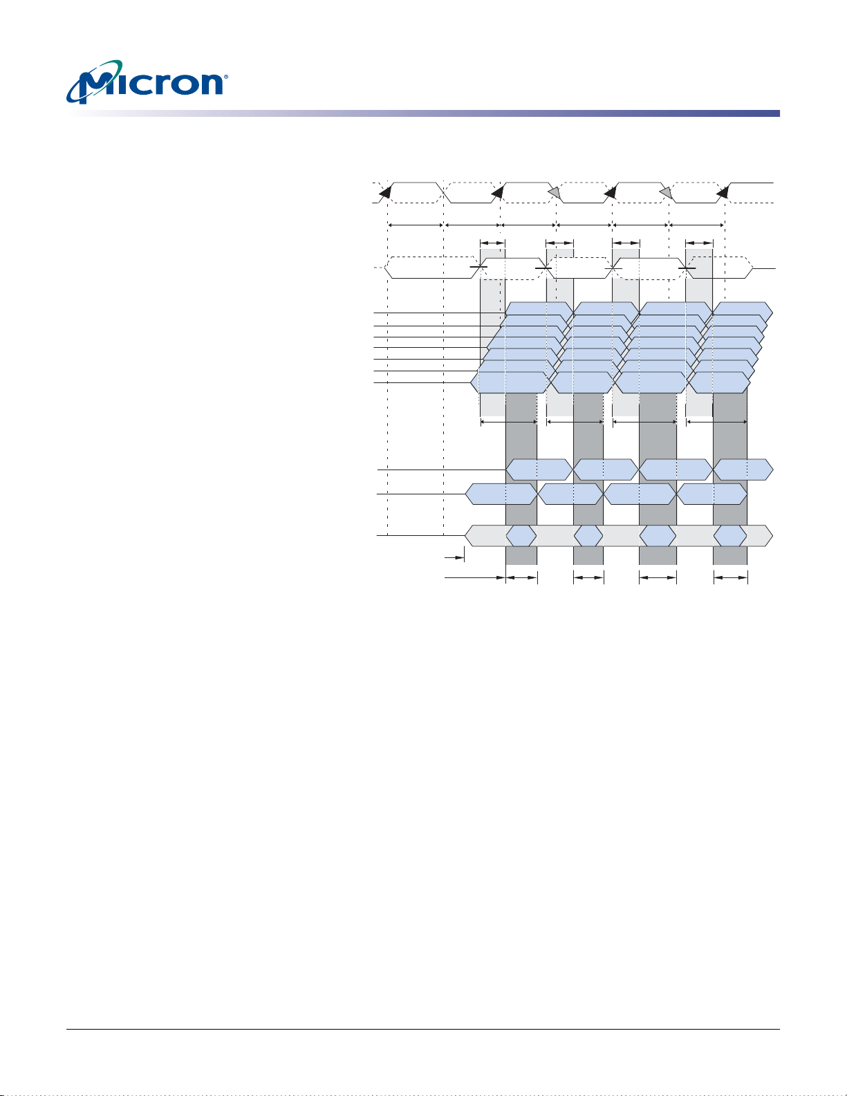
512Mb: x4, x8, x16 DDR2 SDRAM
Figure 27: x4, x8 Data Output Timing – tDQSQ, tQH, and Data Valid Window
T1 T2 T3 T4T2n T3n
CK#
CK
5
t
DQSQ
t
HP
3
DQS#
DQS
5
t
HP
1
5
t
HP
t
DQSQ
5
t
HP
3
t
DQSQ
READs
5
t
HP
3
t
HP
t
DQSQ
5
3
DQ (Last data valid)
DQ
DQ
DQ
DQ
DQ
DQ
2
2
2
2
2
2
DQ (First data no longer valid)
4
t
QH
T2n
T2n
T2n
4
t
QH
T3
T3
T3
4
t
QH
T3n
T3n
T3n
DQ (Last data valid)
DQ (First data no longer valid)
All DQs and DQS, collectively
6
4
t
QH
T2
T2
T2
Earliest signal transition
Latest signal transition
Data
Valid
Window
Data
Valid
Window
Data
Valid
Window
Data
Valid
Window
Notes: 1. DQ transitioning after DQS transition define tDQSQ window. DQS transitions at T2 and at
T2n are “early DQS,” at T3 are “nominal DQS,” and at T3n are “late DQS.”
2. DQ0, DQ1, DQ2, DQ3 for x4 or DQ0–DQ7 for x8.
3.tDQSQ is derived at each DQS clock edge, is not cumu lative over time, begins with DQS
transitions, and ends with the last valid transition of DQ.
t
QH is derived from tHP: tQH = tHP - tQHS.
4.
t
5.
HP is the lesser of tCL or tCH clock transitions collectively when a bank is active.
6. The data valid window is derived for each DQS transition and is defined as
t
QH - tDQSQ.
PDF: 09005aef8117c18e, Source: 09005aef8211b2e6 Micron Technology, Inc., reserves the right to change products or specifications without notice.
512MbDDR2_2.fm - R ev. K 8/06 EN
46 ©2004 Micron Technology, Inc. All rights reserved.
Page 47
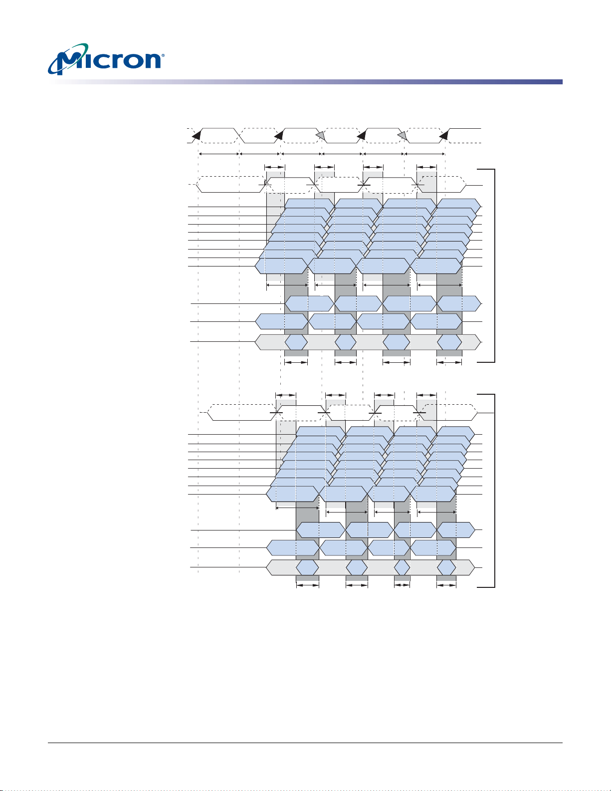
512Mb: x4, x8, x16 DDR2 SDRAM
Figure 28: x16 Data Output Timing – tDQSQ, tQH, and Data Valid Window
T1 T2 T3 T4T2n T3n
CK#
LDSQ#
LDQS
CK
1
5
t
HP
5
t
HP
t
DQSQ
5
t
HP
3
t
DQSQ
5
t
HP
3
t
DQSQ
5
t
HP
3
t
HP
t
DQSQ
READs
5
3
DQ (Last data valid)
DQ (First data no longer valid)
DQ (Last data valid)
DQ (First data no longer valid)
DQ0–DQ7 and LDQS, collectively
DQ (Last data valid)
DQ (First data no longer valid)
DQ (Last data valid)
DQ (First data no longer valid)
DQ8–DQ15 and UDQS, collectively
DQ
DQ
DQ
DQ
DQ
DQ
UDQS#
UDQS
DQ
DQ
DQ
DQ
DQ
DQ
2
2
2
2
2
2
2
2
4
t
QH
2
2
6
1
7
7
7
7
7
7
7
7
7
7
6
Data Valid
t
DQSQ
t
QH
T2
T2
T2
Window
3
4
4
t
QH
T2n
T2n
T2n
Data Valid
Window
3
t
DQSQ
4
t
QH
T2
T2
T2
T2n
T2n
T2n
t
QH
4
Data Valid
Window
t
DQSQ
t
QH
4
t
QH
T3
T3
T3
3
4
T3
T3
T3
t
DQSQ
t
QH
Data Valid
Window
3
4
T3n
T3n
T3n
T3n
T3n
T3n
Lower Byte
Upper Byte
Data Valid
Window
Data Valid
Window
Data Valid
Window
Data Valid
Window
Notes: 1. DQ transitioning after DQS transitions define the tDQSQ window. LDQS defines the lower
byte, and UDQS defines the upper byte.
2. DQ0, DQ1, DQ2, DQ3, DQ4, DQ5, DQ6, or DQ7.
3.tDQSQ is derived at each DQS clock edge, is not cumu lative over time, begins with DQS
transitions, and ends with the last valid transition of DQ.
t
4.
QH is derived from tHP: tQH = tHP - tQHS.
t
HP is the lesser of tCL or tCH clock transitions collectively when a bank is active.
5.
6. The data valid window is derived for each DQS transition and is
t
QH - tDQSQ.
7. DQ8, DQ9, DQ10, D11, DQ12, DQ13, DQ14, or DQ15.
PDF: 09005aef8117c18e, Source: 09005aef8211b2e6 Micron Technology, Inc., reserves the right to change products or specifications without notice.
512MbDDR2_2.fm - R ev. K 8/06 EN
47 ©2004 Micron Technology, Inc. All rights reserved.
Page 48
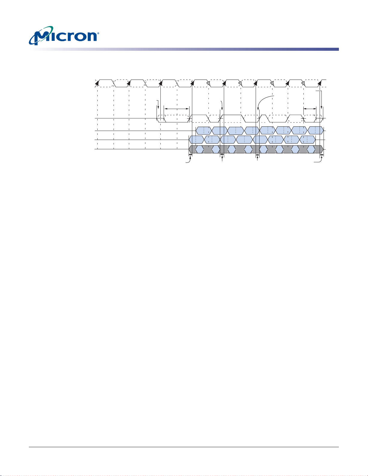
Figure 29: Data Output Timing – tAC and tDQSCK
7
CK#
CK
T0
T1 T2 T3 T3n T4 T4n T5 T5n T6 T6n
t
LZ (MIN)
t
DQSCK1 (MIN)
512Mb: x4, x8, x16 DDR2 SDRAM
READs
T7
t
t
DQSCK1 (MAX)
HZ (MAX)
LDQS#/LDQS / UDQ#/UDQS
DQS#/DQS, or
DQ (Last data valid)
DQ (First data valid)
All DQs collectively
3
Notes: 1.tDQSCK is the DQS output window relative to CK and is the “long-term” component of DQS
t
RPRE
2
t
LZ (MIN)
T3T3T3n T4n T5n T6n
T3n
T3 T4
T3n
tAC4
T4
T4
(MIN)
T4n
T4n
tAC4
(MAX)
T5
T5n
T5
T5n
T5 T6
T6
T6
t
HZ (MAX)
skew.
2. DQ transitioning after DQS transitions define
t
3. All DQ must transition by
t
AC is the DQ output window relative to CK and is the “long term” component of DQ skew.
4.
t
5.
LZ (MIN) and tAC (MIN) are the first valid signal transitions.
t
HZ (MAX) and tAC (MAX) are the latest valid signal transitions.
6.
DQSQ after DQS transitions, regardless of tAC.
t
DQSQ window.
7. READ command with CL = 3, AL = 0 issued at T0.
8. I/O balls, when entering or exiting HIGH-Z, are not referenced to a specific voltage level,
but to when the device begins to drive or no longer drives, respectively.
t
RPST
T6n
T6n
PDF: 09005aef8117c18e, Source: 09005aef8211b2e6 Micron Technology, Inc., reserves the right to change products or specifications without notice.
512MbDDR2_2.fm - R ev. K 8/06 EN
48 ©2004 Micron Technology, Inc. All rights reserved.
Page 49
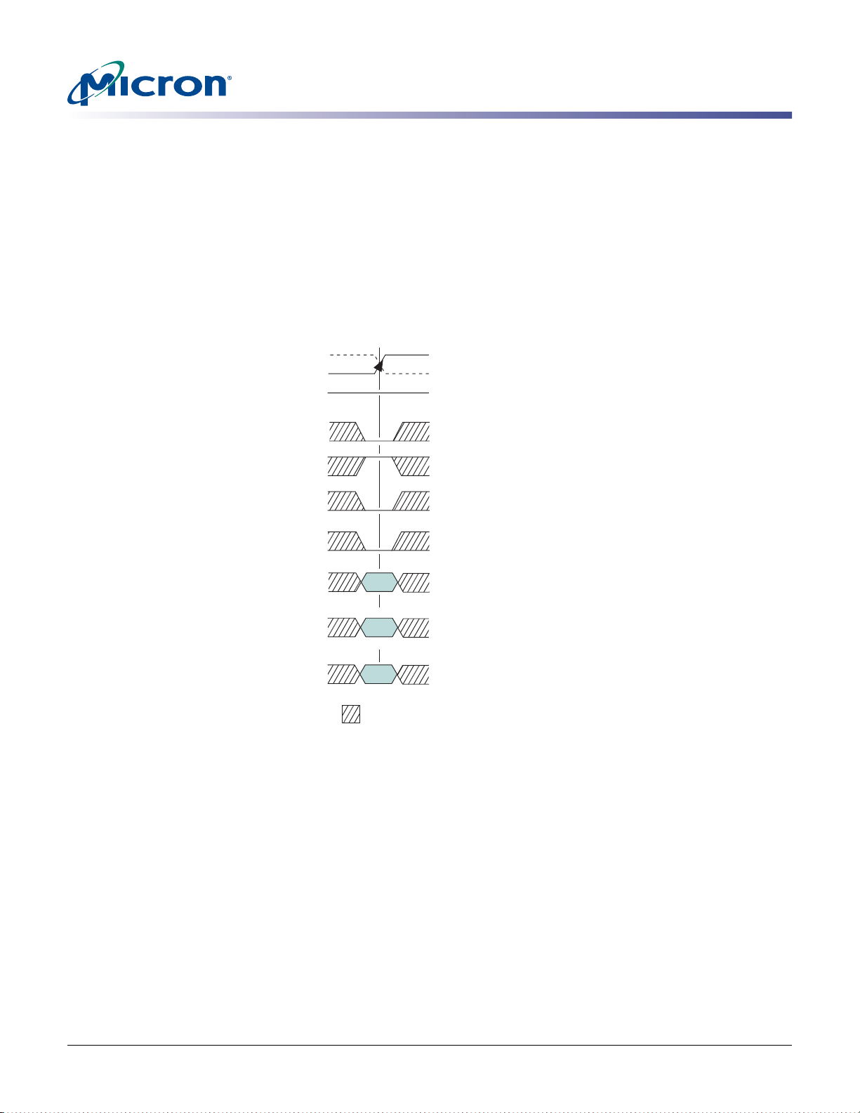
WRITEs
WRITE Command
The WRITE command is used to initiate a burst write access to an active row. The value
on the BA1–BA0 inputs selects the bank, and the address provid ed on inputs A0–i (wher e
i = A9 for x8 and x16; or A9, A11 for x4) selects the starting column location. The value on
input A10 determines whether or not auto precharge is used. If auto precharge is
selected, the row being accessed will be precharged at the end of the WRITE burst; if
auto precharge is not selected, the ro w will remain open for subsequent accesses.
Figure 30: WRITE Command
CK#
CK
CKE
CS#
RAS#
512Mb: x4, x8, x16 DDR2 SDRAM
WRITEs
HIGH
WRITE Operation
CAS#
WE#
ADDRESS
A10
BANK ADDRESS
CA
EN AP
DIS AP
BA
DON’T CARE
Note: CA = column address; BA = bank address; EN AP = enable auto precharge; and DIS AP = dis-
able auto precharge.
Input data appearing on the DQ is written to the memory array subject to the DM input
logic level appearing coincident with the data. If a given DM signal i s r egister ed L O W, the
corresponding data will be written to memory; if the DM signal is registered HIGH, the
corresponding data inputs will be ignored, and a WRITE will not be executed to that
byte/column location (Figure40 on page 58).
WRITE bursts are initiated with a WRITE command, as shown in Figure30. DDR2
SDRAM uses WL equal to RL minus one clock cycle [WL = RL - 1CK = AL + (CL - 1CK)].
The starting column and bank addresses are provided with the WRITE command, and
auto precharge is either enabled or disabled for that acc ess . If auto pr e charge is enab led,
the row being accessed is precharged at the completion of the burst. For the generic
WRITE commands used in the following illustrations, auto precharge is disabled.
PDF: 09005aef8117c18e, Source: 09005aef8211b2e6 Micron Technology, Inc., reserves the right to change products or specifications without notice.
512MbDDR2_2.fm - R ev. K 8/06 EN
49 ©2004 Micron Technology, Inc. All rights reserved.
Page 50
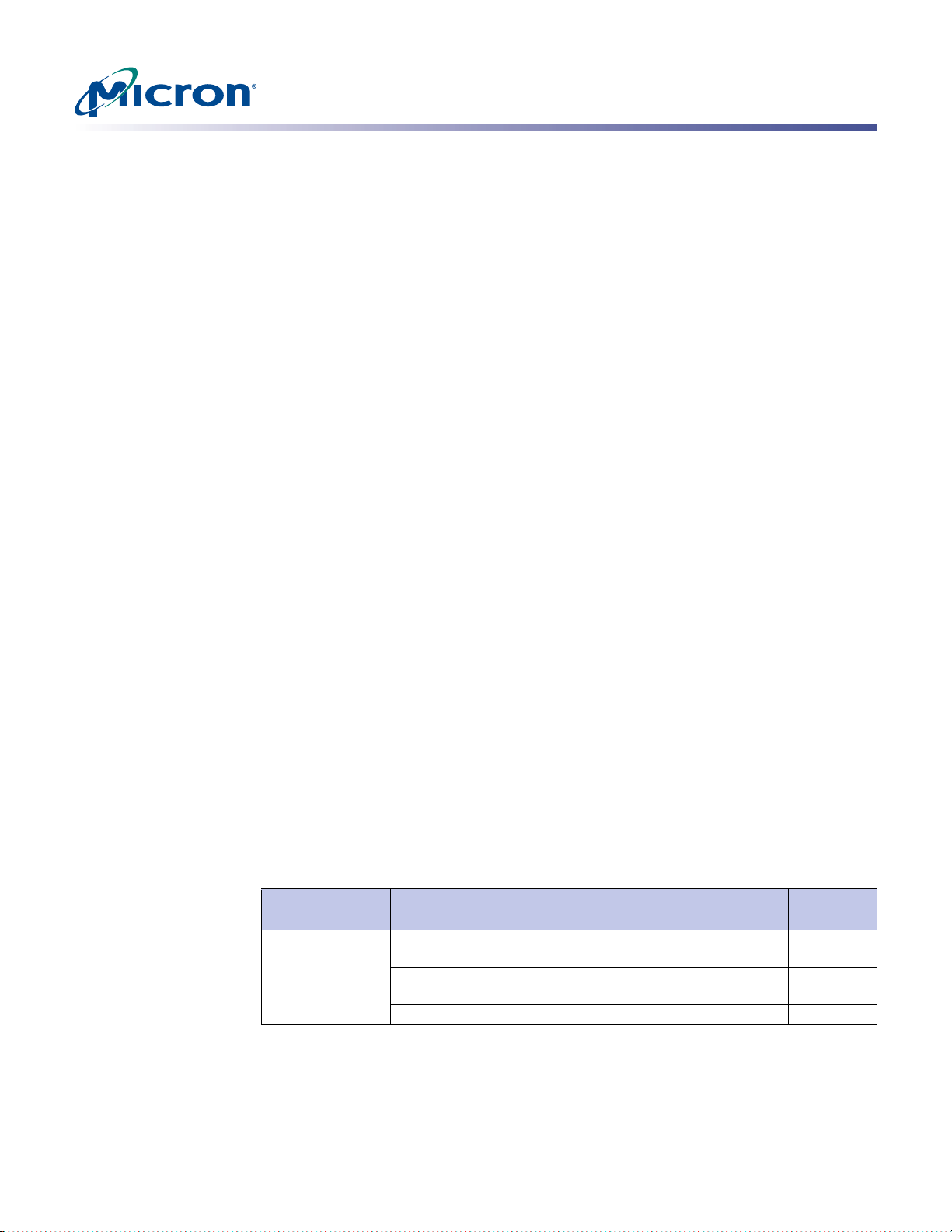
512Mb: x4, x8, x16 DDR2 SDRAM
WRITEs
During WRITE bursts, the first valid data-in element will be registered on the first rising
edge of DQS following the WRITE command, and subsequent data elements will be
registered on successive edges of DQS. The LOW state on DQS between the WRITE
command and the first rising edge is known as the write preamble; the LOW state on
DQS following the last data-in element is known as the write postamble.
The time between the WRITE command and the first rising DQS edge is WL ±
Subsequent DQS positive rising edg es are timed, relative to the associated clock edge, as
t
±
DQSS. tDQSS is specified with a relatively wide range (25 percent of one clock cycle).
All of the WRITE diagrams show the nominal case, and where the two extreme cases
t
(
DQSS [MIN] and tDQSS [MAX]) might not be intuitive, they have also been included.
Figure31 on page 51 shows the nominal case and the extr emes of
t
DQSS for BL = 4. Upon
completion of a burst, assuming no other commands have been initiated, the DQ will
remain High-Z and any additional input data will be ignored.
Data for any WRITE burst may be concatenated with a subsequent WRITE command to
provide continuous flow of input data. The first data element from the new burst is
applied after the last element of a completed burst. The new WRITE command shou ld
be issued x cycles after the first WRITE command, where x equals BL/2.
Figure32 on page 52 shows concatenated bursts of BL = 4. An example of nonconsecutive WRITEs is shown in Figure 33 on page 52. Full-speed random write accesses within a
page or pages can be performed as shown in Figure 34 on page 53. DDR2 SDRAM
supports concurrent auto precharge options, as shown in Table 1 0.
t
DQSS.
DDR2 SDRAM does not allow interrupting or truncating any WRITE burst using BL = 4
operation. Once the BL = 4 WRITE command is registered, it must be allowed to
complete the entire WRITE burst cycle. However, a WRITE BL = 8 operation (with auto
precharge disabled) might be interrupted and trun cat ed ONLY by another WRITE burst
as long as the interruption occurs on a 4-bit boundary, due to the 4n prefetch architecture of DDR2 SDRAM. WRITE burst BL = 8 operations may not be interrupted or truncated with any command except another WRITE command, as shown in Figure35 on
page 53.
Data for any WRITE burst may be followed by a subsequent READ command. To follow a
WRITE,
cycles required to meet
t
WTR should be met, as shown in Figure 36 on page 54. The number of clock
t
WTR is either 2 or tWTR/tCK, whichever is greater. Data for any
WRITE burst may be followed by a subsequent PRECHARGE command.
met, as shown in Figure37 on page 55.
of the data mask condition.
Table 10: WRITE Using Concurrent Auto Precharge
From Command
(Bank n)
WRITE with auto
precharge
To Command
(Bank m)
READ or READ with auto
precharge
WRITE or WRITE with
auto precharge
PRECHARGE or ACTIVE 1
t
t
WR starts at the end of the data burst, regardless
Minimum Delay (with
Concurrent Auto Precharge) Units
t
(CL - 1) + (BL/2) +
(BL/2)
WTR
WR must be
t
CK
t
CK
t
CK
PDF: 09005aef8117c18e, Source: 09005aef8211b2e6 Micron Technology, Inc., reserves the right to change products or specifications without notice.
512MbDDR2_2.fm - R ev. K 8/06 EN
50 ©2004 Micron Technology, Inc. All rights reserved.
Page 51
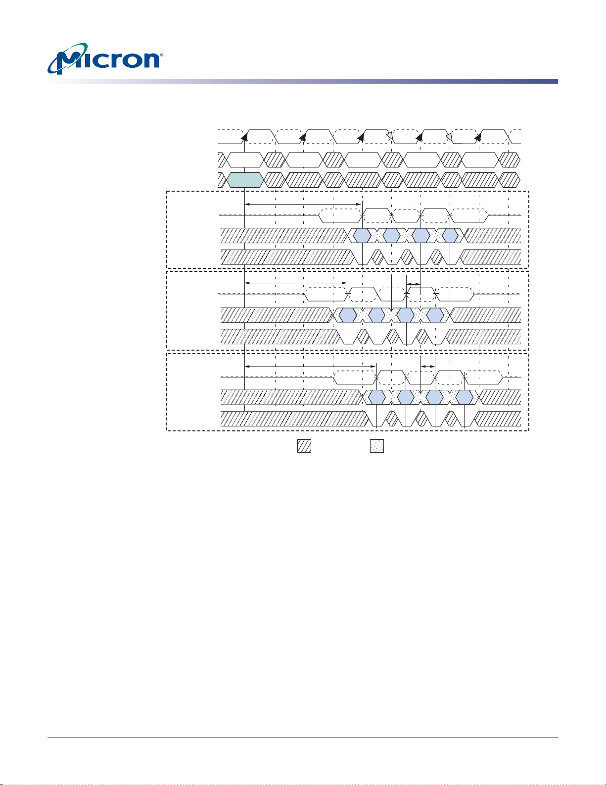
Figure 31: WRITE Burst
512Mb: x4, x8, x16 DDR2 SDRAM
WRITEs
CK#
CK
COMMAND
ADDRESS
t
DQSS (NOM)
DQS, DQS#
DQ
DM
t
DQSS (MIN)
DQS, DQS#
DQ
DM
t
DQSS (MAX)
DQS, DQS#
DQ
T0 T1 T2 T3T2n T4T3n
WRITE NOP NOP
Bank a,
Col b
WL ± tDQSS
DI
b
WL - tDQSS
DI
b
WL + tDQSS
DI
b
NOP NOP
5
t
5
DQSS
t
DQSS
5
DM
Notes: 1. DI b = data-in for column b.
2. Three subsequent elements of data-in are applied in the programmed order following
DI b.
3. Shown with BL = 4, AL = 0, CL = 3; thus, WL = 2.
4. A10 is LOW with the WRITE command (auto precharge is disabled).
5. Subsequent rising DQS signals must align to the clock within
DON’T CARE TRANSITIONING DATA
t
DQSS.
PDF: 09005aef8117c18e, Source: 09005aef8211b2e6 Micron Technology, Inc., reserves the right to change products or specifications without notice.
512MbDDR2_2.fm - R ev. K 8/06 EN
51 ©2004 Micron Technology, Inc. All rights reserved.
Page 52
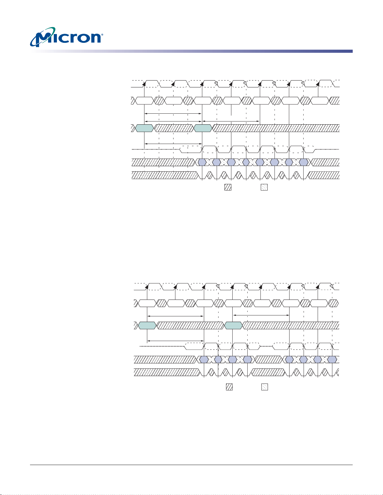
Figure 32: Consecutive WRITE-to-WRITE
512Mb: x4, x8, x16 DDR2 SDRAM
WRITEs
CK#
COMMAND
ADDRESS
t
DQSS (NOM)
DQS, DQS#
DQ
DM
T0 T1 T2 T3T2n T4 T5T4n T6T5nT3nT1n
CK
WRITE NOP WRITE NOP NOP NOP
t
CCD
WL = 2
Bank,
Col b
WL ±
t
DQSS
Bank,
Col n
DI
b
Notes: 1. DI b, etc. = data-in for column b, etc.
2. Three subsequent elements of data-in are applied in the programmed order following
DI b.
3. Three subsequent elements of data-in are applied in the programmed order following
DI n.
4. Shown with BL = 4, AL = 0, CL = 3; thus, WL = 2.
5. Each WRITE command may be to any bank.
6. Subsequent rising DQS signals must align to the clock within
NOP
WL = 2
t
DQSS.
6
6
DON’T CARE TRANSITIONING DATA
6
DI
n
Figure 33: Nonconsecutive WRITE-to-WRITE
CK#
COMMAND
ADDRESS
t
DQSS (NOM) WL ± tDQSS
DQS, DQS#
DQ
DM
Notes: 1. DI b, etc. = data-in for column b, etc.
2. Three subsequent elements of data-in are applied in the programmed order following
DI b.
3. Three subsequent elements of data-in are applied in the programmed order following
DI n.
4. Shown with BL = 4, AL = 0, CL = 3; thus, WL = 2.
5. Each WRITE command may be to any bank.
6. Subsequent rising DQS signals must align to the clock within
T0 T1 T2 T3T2n T4 T5T4nT3n T5n T6 T6n
CK
WRITE NOP NOP NOP NOP NOP
Bank,
Col b
WL = 2
WRITE
WL = 2
Bank,
Col n
6
DI
b
DON’T CARE TRANSITIONING DATA
66
DI
n
t
DQSS.
PDF: 09005aef8117c18e, Source: 09005aef8211b2e6 Micron Technology, Inc., reserves the right to change products or specifications without notice.
512MbDDR2_2.fm - R ev. K 8/06 EN
52 ©2004 Micron Technology, Inc. All rights reserved.
Page 53
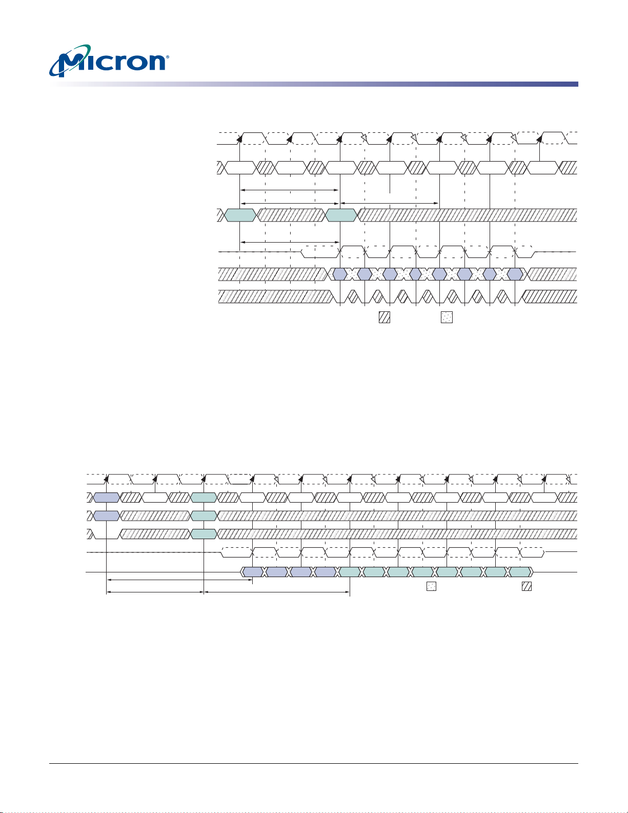
Figure 34: Random WRITE Cycles
512Mb: x4, x8, x16 DDR2 SDRAM
WRITEs
CK#
T0 T1 T2 T3T2n T4 T5T4n T6T5nT3nT1n
CK
COMMAND
WRITE NOP WRITE NOP NOP NOP
t
CCD
WL = 2
ADDRESS
t
DQSS (NOM)
Bank,
Col b
WL ±
t
DQSS
Bank,
Col n
DQS, DQS#
DQ
DM
Notes: 1. DI b, etc. = data-in for column b, etc.
2. Three subsequent elements of data-in are applied in the programmed order following
DI b.
3. Three subsequent elements of data-in are applied in the programmed order following
DI n.
4. Shown with BL = 4, AL = 0, CL = 3; thus, WL = 2.
5. Each WRITE command may be to any bank.
6. Subsequent rising DQS signals must align to the clock within
NOP
WL = 2
6
DI
b
6
DI
n
6
DON’T CARE TRANSITIONING DATA
t
DQSS.
Figure 35: WRITE Interrupted by WRITE
CK#
CK
COMMAND
ADDRESS
A10
DQS, DQS#
DQ
T0 T1 T2
1
WRITE
a
VALID
2
NOP
5
WL = 3
Notes: 1. BL = 8 required and auto precharge must be d isabled (A10 = LOW).
2. WRITE command can be issued to any valid bank and row address (WRITE command at T0
3. Interrupting WRITE command must be issued exactly 2 x tCK from previous WRITE.
4. Auto precharge can be either enabled (A10 = HIGH) or disabled (A10 = LOW) by the in ter-
5. NOP or COMMAND INHIBIT commands are valid. PRECHARGE command cannot be issued to
6. Earliest WRITE-to-PRECHARGE timing for WRITE at T0 is WL + BL/2 +
7. Example shown uses AL = 0; CL = 4, BL = 8.
8. Subsequent rising DQS signals must align to the clock within
3
WRITE
b
2
VALID
4
VALID
and T2 can be either same bank or different bank).
rupting WRITE command.
banks used for WRITEs at T0 and T2.
with T7 and not T5 (since BL = 8 from MR and not the truncated length).
T3 T4 T5 T6
NOP
DIN
a
T7 T8 T9
5
NOP
5
NOP
5
NOP
5
VALID
6
VALID
6
VALID
6
8 8888
D
D
D
D
D
DIN
a + 1
DIN
a + 2
DIN
a + 3
DIN
b
DIN
b + 1
b + 2
IN
IN
IN
b + 4
b + 5
IN
b + 3
WL = 32 clock requirement
t
WR where tWR starts
t
DQSS.
b + 6
D
IN
IN
b + 7
DON’T CARETRANSITIONING DATA
PDF: 09005aef8117c18e, Source: 09005aef8211b2e6 Micron Technology, Inc., reserves the right to change products or specifications without notice.
512MbDDR2_2.fm - R ev. K 8/06 EN
53 ©2004 Micron Technology, Inc. All rights reserved.
Page 54
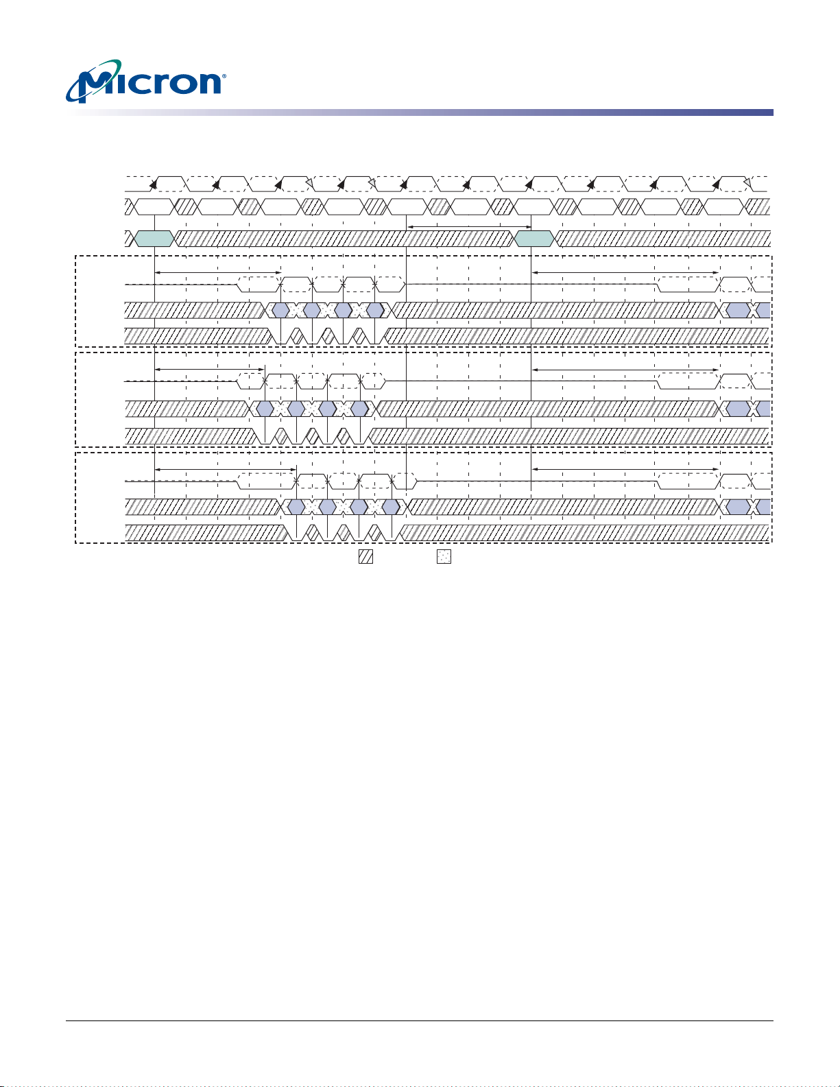
Figure 36: WRITE-to-READ
512Mb: x4, x8, x16 DDR2 SDRAM
WRITEs
CK#
CK
COMMAND
ADDRESS
t
DQSS (NOM)
DQS, DQS#
DQ
DM
t
DQSS (MIN)
DQS, DQS#
DQ
DM
t
DQSS (MAX)
DQS, DQS#
DQ
DM
T0 T1 T2 T3T2n T4 T5 T9nT3n
WRITE NOP NOP NOP NOP NOP NOP NOP
Bank a,
Col b
WL ± tDQSS
DI
b
WL - tDQSS
DI
b
WL + tDQSS
DI
NOP
8
8
8
b
DON’T CARE TRANSITIONING DATA
t
WTR
7
T6 T7 T8 T9
READ
Bank a,
Col n
CL = 3
CL = 3
CL = 3
Notes: 1. DI b = data-in for column b; DOUT n = data-out from column n.
2. BL = 4, AL = 0, CL = 3; thus, WL = 2.
3. One subsequent element of data-in is applied in the programmed order following DI b.
t
WTR is referenced from the first positive CK edge after the last data-in pair.
4.
5. A10 is LOW with the WRITE command (auto precharge is disabled).
6. The number of clock cycles required to meet tWTR is either 2 or tWTR/tCK, whichever is
greater.
t
WTR is required for any READ following a WRITE to the same device, but it is not required
7.
between module ranks.
t
8. Subsequent rising DQS signals must align to the clock within
DQSS.
Dout
Dout
Dout
PDF: 09005aef8117c18e, Source: 09005aef8211b2e6 Micron Technology, Inc., reserves the right to change products or specifications without notice.
512MbDDR2_2.fm - R ev. K 8/06 EN
54 ©2004 Micron Technology, Inc. All rights reserved.
Page 55
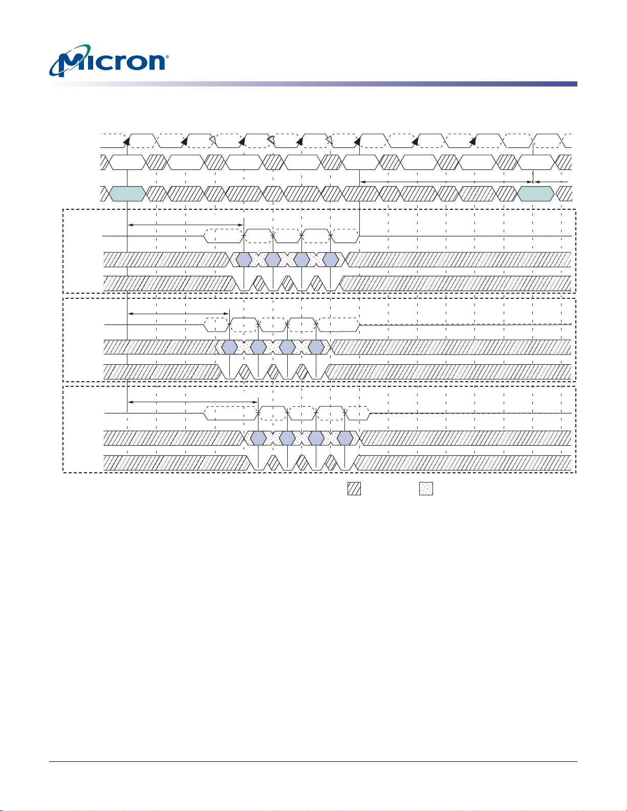
Figure 37: WRITE-to-PRECHARGE
512Mb: x4, x8, x16 DDR2 SDRAM
WRITEs
CK#
CK
COMMAND
ADDRESS
t
DQSS (NOM)
DQS#
DQS
DQ
DM
t
DQSS (MIN)
DQS#
DQS
DQ
DM
t
DQSS (MAX)
DQS#
DQS
DQ
T0 T1 T2 T3T2n T4 T5T3n
WRITE NOP NOP NOP NOPNOP
Bank a,
Col b
WL + tDQSS
DI
b
WL - tDQSS
DI
b
WL + tDQSS
DI
b
NOP
8
8
8
T6 T7
t
WR
7
PRE
t
Bank,
(a or all)
RP
DM
Notes: 1. DI b = data-in for column b.
2. Three subsequent elements of data-in are applied in the pro gra mmed order following DI b.
3. BL = 4, CL = 3, AL = 0; thus, WL = 2.
t
WR is referenced from the first positive CK edge after the last data-in pair.
4.
5. The PRECHARGE and WRITE commands are to the same bank. However, the PRECHARGE
and WRITE commands may be to different banks, in which case
PRECHARGE command could be applied earlier.
6. A10 is LOW with the WRITE command (auto precharge is disabled).
7. PRE = PRECHARGE command.
8. Subsequent rising DQS signals must align to the clock within
DON’T CARE TRANSITIONING DATA
t
WR is not required and the
t
DQSS.
PDF: 09005aef8117c18e, Source: 09005aef8211b2e6 Micron Technology, Inc., reserves the right to change products or specifications without notice.
512MbDDR2_2.fm - R ev. K 8/06 EN
55 ©2004 Micron Technology, Inc. All rights reserved.
Page 56
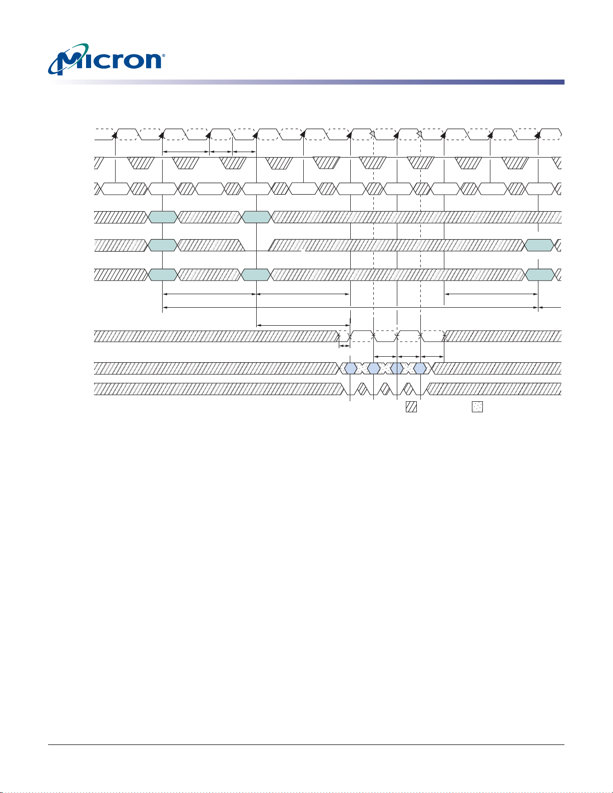
Figure 38: Bank Write – without Auto Precharge
512Mb: x4, x8, x16 DDR2 SDRAM
WRITEs
CK#
CK
CKE
COMMAND
ADDRESS
A10
BA0, BA1
DQS, DQS#
DQ
DM
T0
5
1
NOP
6
T1
t
ACT
RA Col n
RA
Bank x
T2 T3 T5 T6 T6n T7 T8 T9T5n
t
RCD
t
RAS
NOP
tCHt
6
CL
CK
WRITE
3
Bank x
2
T4
6
NOP
WL = 2
WL ± tDQSS (NOM)
NOP
t
WPRE
DI
n
6
NOP
9
t
DQSLtDQSHtWPST
6
DON’T CARE TRANSITIONING DATA
NOP
6
NOP
t
WR
6
PRE
ALL BANKS
ONE BANK
4
Bank x
t
RP
Notes: 1. DI n = data-in from column n; subsequent elements are applied in the programmed order.
2. BL = 4, AL = 0, and WL = 2 in the case shown.
3. Disable auto precharge.
4. “Don’t Care” if A10 is HIGH at T9.
5. PRE = PRECHARGE, ACT = ACTIVE, RA = row address, BA = bank address.
6. NOP commands are shown for ease of illustration; other commands may be valid at these
times.
7.tDSH is applicable during tDQSS (MIN) and is referenced from CK T5 or T6.
t
DSS is applicable during tDQSS (MAX) and is referenced from CK T6 or T7.
8.
9. Subsequent rising DQS signals must align to the clock within
t
DQSS.
PDF: 09005aef8117c18e, Source: 09005aef8211b2e6 Micron Technology, Inc., reserves the right to change products or specifications without notice.
512MbDDR2_2.fm - R ev. K 8/06 EN
56 ©2004 Micron Technology, Inc. All rights reserved.
Page 57
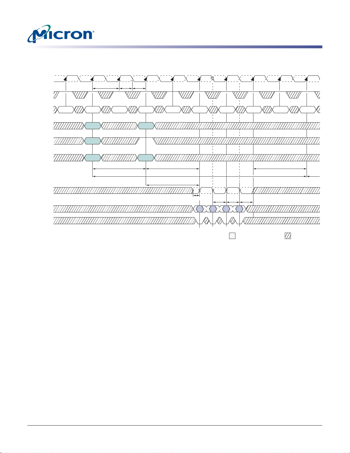
Figure 39: Bank Write – with Auto Precharge
512Mb: x4, x8, x16 DDR2 SDRAM
WRITEs
CK#
CK
CKE
COMMAND
ADDRESS
A10
BA0, BA1
DQS,DQS#
DQ
DM
T0
4
1
NOP
5
T1
t
ACT
RA Col n
RA
Bank x
T2 T3 T4 T5 T5n T6 T7 T8T6n
t
t
RCD
RAS
NOP
tCHt
5
CL
CK
WRITE
3
Bank x
2
NOP
WL = 2
WL ± tDQSS (NOM)
T9
5
NOP
t
WPRE
DI
5
n
5
NOP
9
t
DQSLtDQSHtWPST
TRANSITIONING DATA
NOP
5
WR
8
NOP
5
DON’T CARE
NOP
5
t
RP
Notes: 1. DI n = data-in from column n; subsequent elements are applied in the programmed order.
2. BL = 4, AL = 0, and WL = 2 in the case shown.
3. Enable auto precharge.
4. ACT = ACTIVE, RA = row address, BA = bank address.
5. NOP commands are shown for ease of illustration; other commands may be valid at these
times.
t
DSH is applicable during tDQSS (MIN) and is referenced from CK T5 or T6.
6.
t
7.
DSS is applicable during tDQSS (MAX) and is referenced from CK T6 or T7.
8. WR is programmed via MR[11, 10, 9] and is calculated by dividing
t
CK and rounding up to the next integer value.
9. Subsequent rising DQS signals must align to the clock within
t
WR (in nanoseconds) by
t
DQSS.
PDF: 09005aef8117c18e, Source: 09005aef8211b2e6 Micron Technology, Inc., reserves the right to change products or specifications without notice.
512MbDDR2_2.fm - R ev. K 8/06 EN
57 ©2004 Micron Technology, Inc. All rights reserved.
Page 58
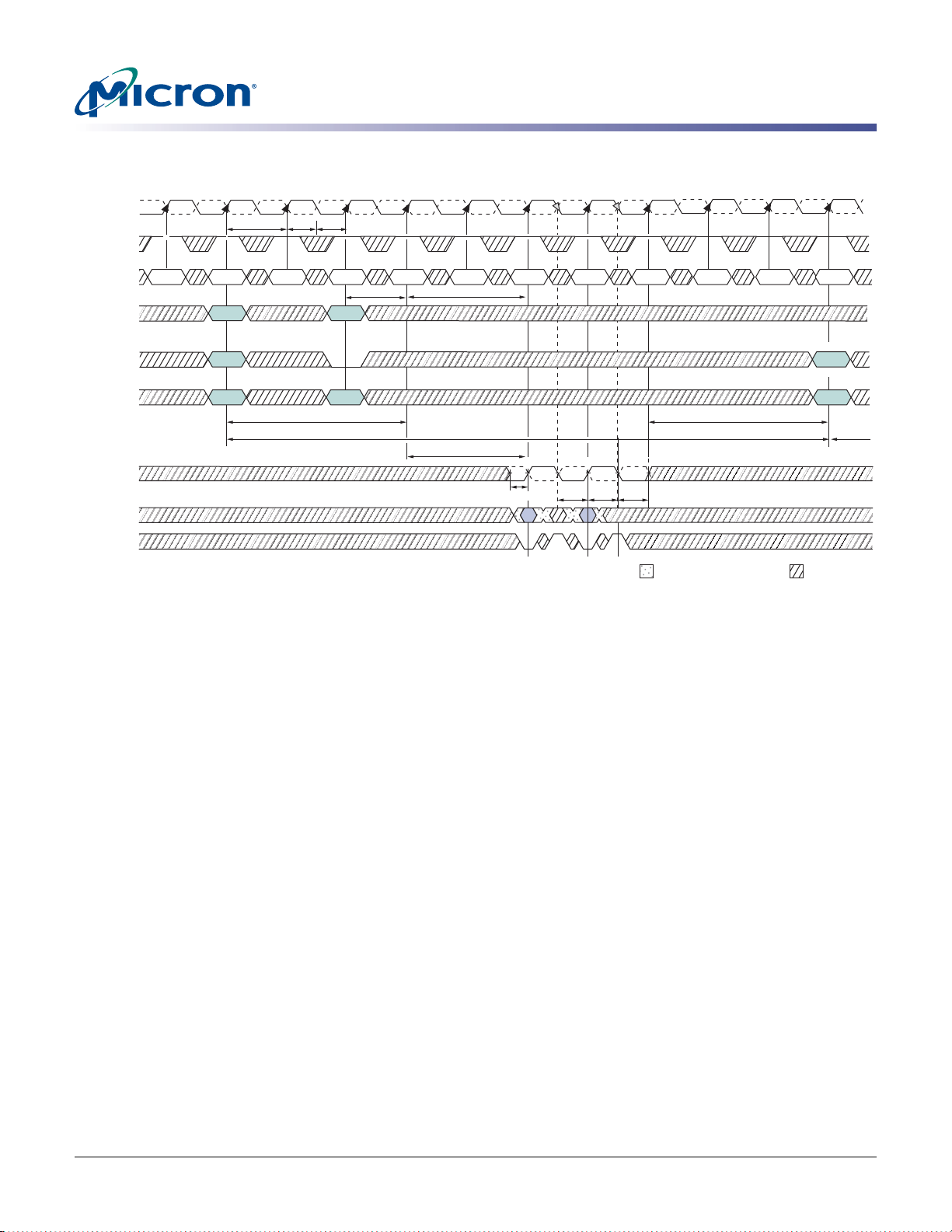
Figure 40: WRITE – DM Operation
512Mb: x4, x8, x16 DDR2 SDRAM
WRITEs
CK#
CK
CKE
COMMAND
ADDRESS
A10
BA0, BA1
DQS, DQS#
DQ
DM
T0
5
NOP
1
T1
t
CK
6
ACT
RA Col n
RA
Bank x
T2 T3 T4 T5 T7nT6 T7 T8T6n
tCHt
CL
6
NOP
WL = 2
WL ± tDQSS (NOM)
t
WPRE
NOP
t
RCD
t
RAS
NOP
6
WRITE
3
Bank x
2
AL = 1
NOP
6
6
DI
n
6
NOP
10
t
DQSLtDQSHtWPST
NOP
T9 T10 T11
6
NOP
t
WR
6
9
NOP
6
ALL BANKS
ONE BANK
DON’T CARETRANSITIONING DATA
PRE
Bank x
4
t
RP
A
Notes: 1. DI n = data-in from column n; subsequent elements are applied in the programmed order.
2. Burst length = 4, AL = 1, and WL = 2 in the case shown.
3. Disable auto precharge.
4. “Don’t Care” if A10 is HIGH at T11.
5. PRE = PRECHARGE, ACT = ACTIVE, RA = row address, BA = bank address.
6. NOP commands are shown for ease of illustration; other commands may be valid at these
times.
t
DSH is applicable during tDQSS (MIN) and is referenced from CK T6 or T7.
7.
t
8.
DSS is applicable during tDQSS (MAX) and is referenced from CK T7 or T8.
t
WR starts at the end of the data burst regardless of the data mask condition.
9.
10. Subsequent rising DQS signals must align to the clock within
t
DQSS.
PDF: 09005aef8117c18e, Source: 09005aef8211b2e6 Micron Technology, Inc., reserves the right to change products or specifications without notice.
512MbDDR2_2.fm - R ev. K 8/06 EN
58 ©2004 Micron Technology, Inc. All rights reserved.
Page 59
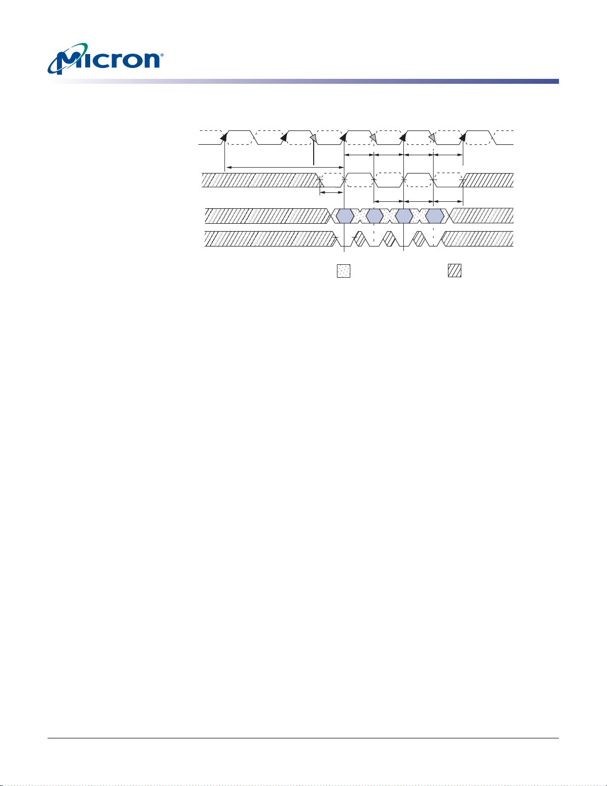
Figure 41: Data Input Timing
512Mb: x4, x8, x16 DDR2 SDRAM
WRITEs
CK#
CK
WL - tDQSS (NOM)
DQS
DQS#
DQ
DM
T1T0 T1n T2 T2n T3 T4T3n
1
t
DSH
t
WPRE
DI
TRANSITIONING DATA
Notes: 1.tDSH (MIN) generally occurs during tDQSS (MIN).
t
2.
DSS (MIN) generally occurs during tDQSS (MAX).
3. WRITE command issued at T0.
4. For x16, LDQS controls the lower byte and UDQS controls the upper byte.
5. WRITE command with WL = 2 (CL = 3, AL = 0) issued at T0.
6. Subsequent rising DQS signals must align to the clock within
t
DSS
t
DQSL
2
6
t
DSH
t
DQSH
1
t
t
DQSS.
t
DSS
WPST
2
DON’T CARE
PDF: 09005aef8117c18e, Source: 09005aef8211b2e6 Micron Technology, Inc., reserves the right to change products or specifications without notice.
512MbDDR2_2.fm - R ev. K 8/06 EN
59 ©2004 Micron Technology, Inc. All rights reserved.
Page 60
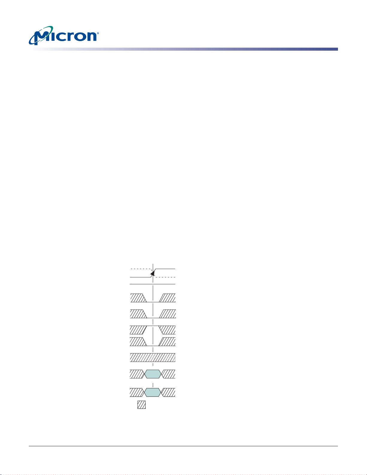
Precharge
PRECHARGE Command
The PRECHARGE command, illustrated in Figur e42 on page 60, is used to deactivate the
open row in a particular bank or the open row in all banks. The bank(s) will be available
for a subsequent row activation a specified time (
is issued, except in the case of concurrent auto precharge, where a READ or WRITE
command to a different bank is allowed as long as it does not interrupt the data transfer
in the current bank and does not violate any other timing parameters. Once a bank has
been precharged, it is in the idle state and must be activated prior to any READ or WRITE
commands being issued to that bank. A PRECHARGE command is allowed if there is no
open row in that bank (idle state) or if the previously open row is already in the process
of precharging. However, the precharge period will be determined by the last
PRECHARGE command issued to the bank.
PRECHARGE Operation
Input A10 determines whether one or all banks are to be precharged, and in the case
where only one bank is to be precharged, inputs BA1–BA0 select the bank. Otherwise
BA1–BA0 are treated as “Don’t Care.”
512Mb: x4, x8, x16 DDR2 SDRAM
Precharge
t
RP) after the PRECHARGE command
When all banks are to be precharged , inputs BA1–BA0 ar e tr eated as “Don’t C ar e . ” Once a
bank has been precharged, it is in the idle state and must be activated prior to any READ
or WRITE commands being issued to that bank.
PRECHARGE (ALL) command is issued, regardless of the number of banks already open
or closed. If a single-bank PRECHARGE command is issued,
Figure 42: PRECHARGE Command
CK#
CK
CKE
CS#
RAS#
CAS#
WE#
ADDRESS
A10
HIGH
ALL BANKS
ONE BANK
t
RPA timing applies when the
t
RP timing applies.
BA0, BA1
Note: BA = bank address (if A10 is LOW; otherwise “Don’t Care”).
PDF: 09005aef8117c18e, Source: 09005aef8211b2e6 Micron Technology, Inc., reserves the right to change products or specifications without notice.
512MbDDR2_2.fm - R ev. K 8/06 EN
BA
DON’T CARE
60 ©2004 Micron Technology, Inc. All rights reserved.
Page 61

Self Refresh
SELF REFRESH Command
The SELF REFRESH command can be used to retain data in the DDR2 SDRAM, even if
the rest of the system is powered down. When in the self refresh mode, the DDR2
SDRAM retains data without external clocking. All power supply inputs (including V
must be maintained at valid levels upon entry/exit and during SELF REFRESH operation.
The SELF REFRESH command is initiated like a REFRESH command exc ept CKE is L O W.
The DLL is automatically disabled upon entering self refresh and is automatically
enabled upon exiting self refresh (200 clock cycles must then occur before a READ
command can be issued). The differential clock should remain stable and meet
specifications at least 1 x
input signals except CKE are “Don’t Care” during self refresh.
512Mb: x4, x8, x16 DDR2 SDRAM
Self Refresh
REF)
t
t
CK after entering self refr esh mode. All command and address
CKE
The procedure for exiting self refresh requires a sequence of commands. First, the differential clock must be stable and meet
going back HIGH. Once CKE is HIGH (
registrations), the DDR2 SDRAM must have NOP or DESELECT commands issued for
t
XSNR because time is required for the completion of any internal refresh in progress. A
t
CK specifications at least 1 x tCK prior to CKE
t
CKE [MIN] has been satisfied with four clock
simple algorithm for meeting both refresh and DLL requirements is to apply NOP or
DESELECT commands for 200 clock cycles before applying any other command.
PDF: 09005aef8117c18e, Source: 09005aef8211b2e6 Micron Technology, Inc., reserves the right to change products or specifications without notice.
512MbDDR2_2.fm - R ev. K 8/06 EN
61 ©2004 Micron Technology, Inc. All rights reserved.
Page 62
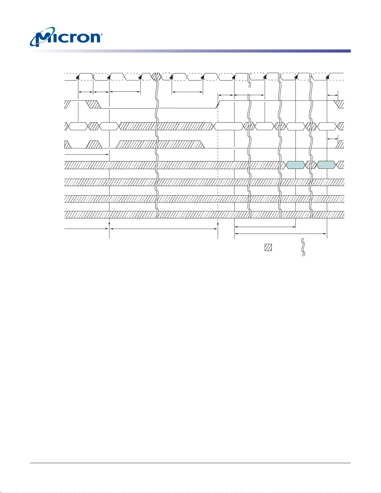
512Mb: x4, x8, x16 DDR2 SDRAM
Self Refresh
Figure 43: Self Refresh
CK#
CK
CKE
COMMAND
ODT
ADDRESS
DQS#,
DQS
DQ
DM
T0 T1 Ta2Ta1
1
1
5
8
t
CHtCL
NOP REF
t
AOFD / tAOFPD
2
t
RP
Enter self refresh
mode (synchronous)
XSRD
VALID
VALID
4,6
Tc0Tb0
3
t
CKE (MIN)
Ta0
tCK1
9
t
6
ISXR
7
NOP
Exit self refresh
mode (asynchronous)
t
CKE
10
t
NOP
XSNR
7
3, 6, 11
t
DON’T CARE
T2
tCK1
8
Td0
t
IH
3
VALID
t
IH
4
VALID
Indicates a break in
time scale
Notes: 1. Clock must be stable and meeting tCK specifications at least 1 x tCK after entering self
refresh mode and at least 1 x tCK prior to exiting self refresh mode.
2. Device must be in the all banks idle state prior to entering self refresh mode.
3.tXSNR is required before any non-READ command can be applied.
t
XSRD (200 cycles of CK) is required before a READ command can be applied at state Td0.
4.
5. REF = REFRESH command.
t
6. Self refresh exit is asynchronous; however,
XSNR and tXSRD timing starts at the first rising
clock edge where CKE HIGH satisfies tISXR.
7. NOP or DESELECT commands are required prior to exiting self refresh until state Tc0, which
allows any non-READ command.
8. ODT must be disabled and R
TT off (
AOFD and tAOFPD have been satisfied) prior to entering
t
SELF REFRESH at state T1.
9. Once self refresh has been entered,
t
10. CKE must stay HIGH until
XSRD is met; however , if self refresh is being re-entered, CKE may
t
CKE (MIN) must be satisfied prior to exiting self refresh.
go back LOW after tXSNR is satisfied.
11. Once exiting SELF REFRESH, ODT must remain LOW until
t
XSRD is satisfied.
PDF: 09005aef8117c18e, Source: 09005aef8211b2e6 Micron Technology, Inc., reserves the right to change products or specifications without notice.
512MbDDR2_2.fm - R ev. K 8/06 EN
62 ©2004 Micron Technology, Inc. All rights reserved.
Page 63
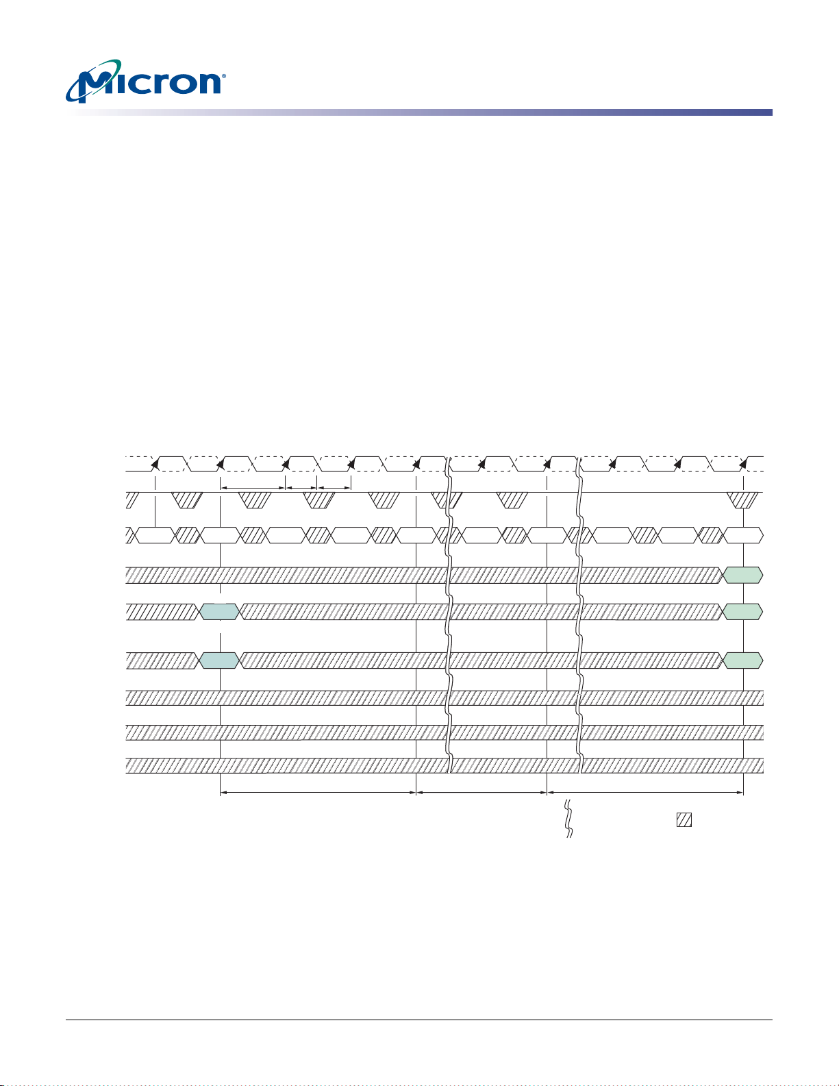
REFRESH
REFRESH Command
REFRESH is used during normal operation of the DDR2 SDRAM and is analogous to
CAS#-Before-RAS# (CBR) REFRESH. This command is nonpersistent, so it must be
issued each time a refr esh is r equired. The addr essing is gener ated by the internal r efre sh
controller. This makes the address bits a “Don’t Care” during an REFRESH command.
The 512Mb DDR2 SDRAM requires REFRESH cycles at an average interval of 7.8125µs
(MAX). To allow for improved efficiency in scheduling and switching between tasks,
some flexibility in the absolute refresh interval is provided. A maximum of eight
REFRESH commands can be posted (to defer issuing REFRESH commands) to any given
DDR2 SDRAM, meaning that the maximum absolute interval between any REFRESH
command and the next REFRESH command is 9 × 7.8125µs (70.3µs; 3.9µs for hightemperature operation). The refresh period begins when the REFRESH command is
registered and ends
Figure 44: Refresh Mode
t
RFC (MIN) later.
512Mb: x4, x8, x16 DDR2 SDRAM
REFRESH
CK#
CK
CKE
COMMAND
ADDRESS
A10
BANK
DQS, DQS#
DQ
DM
T0
1
1
1
4
4
4
NOP
2
T1
PRE
ALL BANKS
ONE BANK
3
Bank(s)
t
CK
T2 T3
t
CHtCL
2
NOP
t
RP
NOP
2
T4
REF NOP
Ta0
2
t
RFC(MIN)
Ta1
REF
Tb0
5
NOP
Indicates a break in
time scale
Tb1 Tb2
2
t
RFC
NOP
5
2
DON’T CARE
ACT
RA
RA
BA
Notes: 1. PRE = PRECHARGE, ACT = ACTIVE, AR = REFRESH, RA = row address, BA = bank address.
2. NOP commands are shown for ease of illustration; other valid commands may be possible at
these times. CKE must be active during clock positive transitions.
3. “Don’t Care” if A10 is HIGH at this point; A10 must be HIGH if more than one bank is active
(i.e., must precharge all active banks).
4. DM, DQ, and DQS signals are all “Don’t Care”/High-Z for operations shown.
5. The second REFRESH is not required and is only shown as an example o f two back-to-back
REFRESH commands.
PDF: 09005aef8117c18e, Source: 09005aef8211b2e6 Micron Technology, Inc., reserves the right to change products or specifications without notice.
512MbDDR2_2.fm - R ev. K 8/06 EN
63 ©2004 Micron Technology, Inc. All rights reserved.
Page 64

Power-Down Mode
DDR2 SDRAMs support multiple power-down modes that allow significant power
savings over normal operating modes. CKE is used to enter and exit different powerdown modes. Power-down entry and exit timings are shown in Figure45 on page 65.
Detailed power-down entry conditions are shown in Figures46 through 53. The CKE
Truth Table, Table 11, is shown on page 66.
DDR2 SDRAMs requir e CKE to be registered HIGH (active) at all times that an access is
in progress—from the issuing of a READ or WRITE command until completion of the
burst. Thus, a clock suspend is not supported. For READs, a burst completion is defined
when the read postamble is satisfied; for WRITEs, a burst completion is defined when
the write postamble and
page 68. The number of clock cycles required to meet
whichever is greater.
Power-down mode (see Figure45 on page 65) is entered when CKE is registered LOW
coincident with a NOP or DESELECT command. CKE is not allowed to go LOW during a
mode register or extended mode register command time, or while a READ or WRITE
operation is in progress. If power-down occurs when all banks are idle, this mode is
referred to as precharge power -down. If po wer -down occurs when there is a ro w active in
any bank, this mode is referred to as active power-down. Entering power-down deactivates the input and output buffers, excluding CK, CK#, ODT, and CKE. For maximum
power savings, the DLL is frozen during precharge power-down. Exiting active powerdown requires the device to be at the same voltage and frequency as when it entered
power-down. Exiting precharge power-d own requires the device to be at the same
voltage as when it entered power-down; however, the clock frequency is allowed to
change. See “Precharge Power-Down Clock FrequencyChange” on page71.
512Mb: x4, x8, x16 DDR2 SDRAM
Power-Down Mode
t
WR or tWTR are satisfied, as shown in Figures48 and 49 on
t
WTR is either two or tWTR/tCK,
The maximum duration for either active or precharge power-down is limited by the
refresh requirements of the device
entry and exit is limited by the
t
RFC (MAX). The minimum duration for po wer-down
t
CKE (MIN) parameter. While in power-down mode, CKE
LOW, a stable clock signal, and stable power supply signals must be maintained at the
inputs of the DDR2 SDRAM, while all other input signals are “Don’t Care” except ODT.
Detailed ODT timing diagrams for differ ent power-down modes are shown in F i gures56
through 63.
The power-down state is synchronously exited when CKE is registered HIGH (in
conjunction with an NOP or DESELECT command), as shown in Figure45 on page 65.
PDF: 09005aef8117c18e, Source: 09005aef8211b2e6 Micron Technology, Inc., reserves the right to change products or specifications without notice.
512MbDDR2_2.fm - R ev. K 8/06 EN
64 ©2004 Micron Technology, Inc. All rights reserved.
Page 65
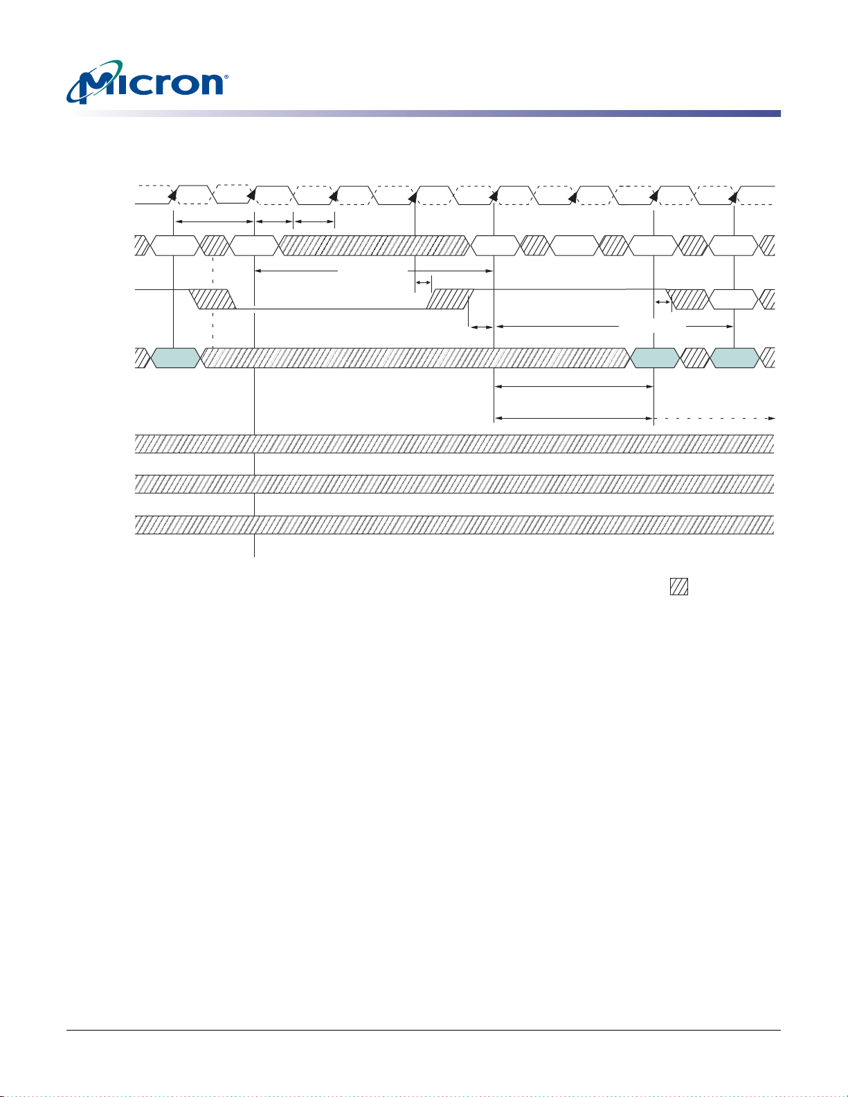
Figure 45: Power-Down
T1 T2 T3 T4 T5 T6 T7 T8
CK#
CK
t
CK
t
CHtCL
512Mb: x4, x8, x16 DDR2 SDRAM
Power-Down Mode
COMMAND
CKE
ADDRESS
DQS, DQS#
DQ
DM
1
VALID
NOP NOP NOP
Enter
power-down
mode
2
t
CKE (MIN)
3
t
IH
t
IS
Exit
power-down
mode
tXP4
t
, tXARD
XARDS
5
6
VALID
t
IH
t
CKE (MIN)
3
VALID VALID
DON’T CARE
Notes: 1. If this command is a PRECHARGE (or if the device is already in the idle state), then the
power-down mode shown is precharge power-down. If this command is an ACTIVE (or if at
least one row is already active), then the power-down mode shown is active power-down.
2. No column accesses are allowed to be in progress at the time power-down is entered. If the
DLL was not in a locked state when CKE went LOW, the DLL must be reset after exiting
power-down mode for proper READ operation.
t
CKE (MIN) of three clocks means CKE must be registered on three consecutive positive clock
3.
edges. CKE must remain at the valid input level the entire time it takes to achieve the three
clocks of registration. Thus, after any CKE transition, CKE may not transition from its valid
level during the time period of
t
IH window.
t
XP timing is used for exit precharge power-down and active power-down to any non-READ
4.
t
IS + 2 x tCK + tIH. CKE must not transition during its tIS and
command.
t
5.
XARD timing is used for exit active power-down to READ command if fast exit is selected
via MR (bit 12 = 0).
t
XARDS timing is used for exit active power-down to READ command if slow exit is selected
6.
via MR (bit 12 = 1).
VALIDVALID
PDF: 09005aef8117c18e, Source: 09005aef8211b2e6 Micron Technology, Inc., reserves the right to change products or specifications without notice.
512MbDDR2_2.fm - R ev. K 8/06 EN
65 ©2004 Micron Technology, Inc. All rights reserved.
Page 66
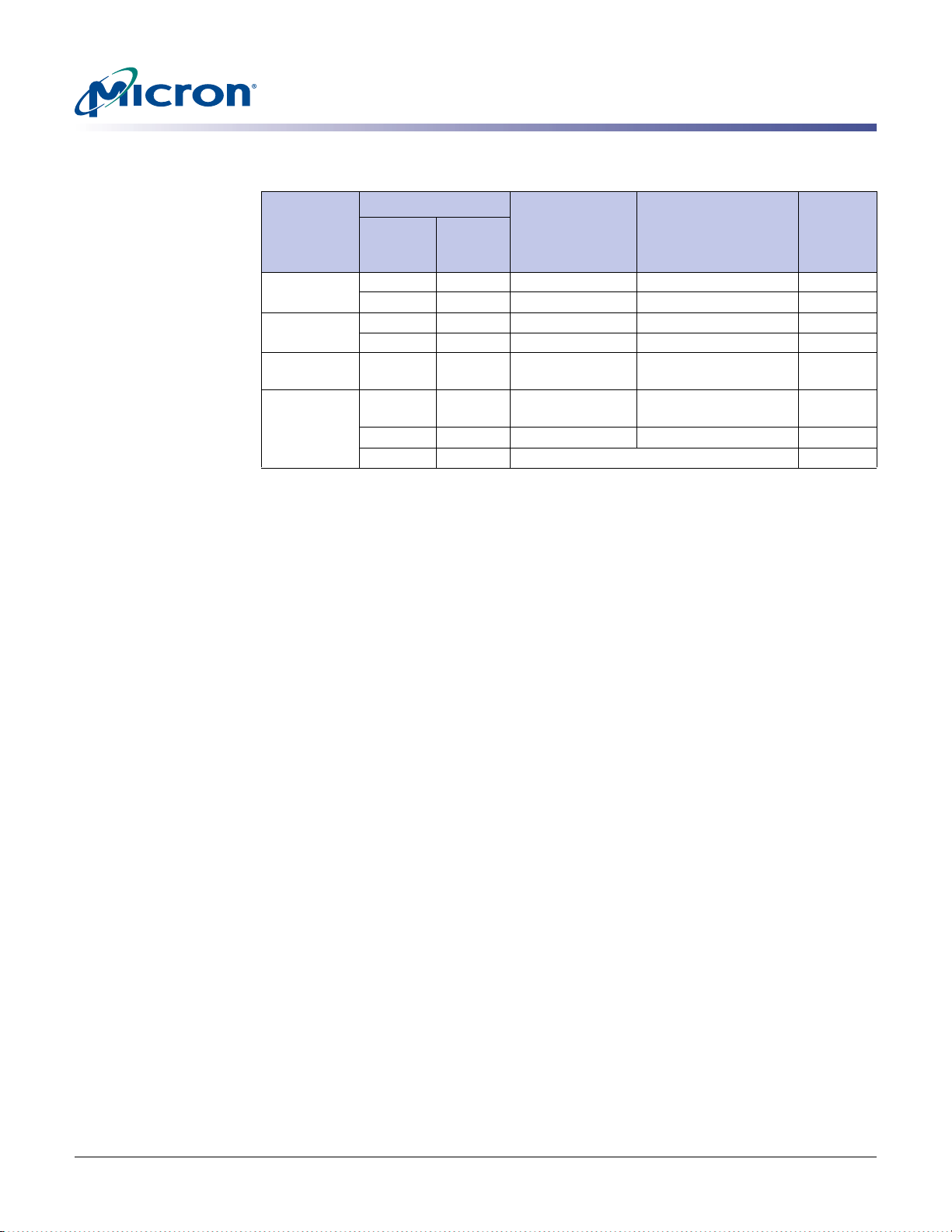
Table 11: CKE Truth Table
Notes 1–3, 12
Power-down L L X Maintain power-down 13, 14
Self refresh L L X Maintain self refresh 14
Bank(s) active H L DESELECT or NOP Active power-down
All banks idle H L DESELECT or NOP Precharge power-down
Notes: 1. CKE (n) is the logic state of CKE at clock edge n; CKE (n-1) was the state of CKE at the previ-
2. Current state is the state of the DDR2 SDRAM immedi ately prior to clock edge n.
3. Command (n) is the command registered at clock edge n, and action (n) is a result of com-
4. All states and sequences not shown are ille ga l or reserved unless explicitly described else-
5. On self refresh exit, DESELECT or NOP commands must be issued on every clock edge occur-
6. Self refresh mode can only be entered from the all banks idle state.
7. Must be a legal com mand as defined in the Command Truth Table, Table 5 on page 29.
8. Valid commands for power-down entry and exit are NOP and DESELECT only.
9. Valid commands for self refresh exit are NOP and DESELECT only.
10. Power-down and self refresh can not be entered while READ or WRITE operations, LOAD
11. Minimum CKE HIGH time is
12. The state of ODT does not affect the states described in this table. The ODT function is not
13. Power-down modes do not perform any REFRESH operations. The duration of power-down
14. “X” means “Don’t Care” (including floating around V
512Mb: x4, x8, x16 DDR2 SDRAM
Power-Down Mode
CKE
Current
State
Cycle
(n-1)
Current
Cycle (n)
L H DESELECT or NOP Power-down exit 4, 8
L H DE SELECT or NOP Self refresh exit 4, 5, 9
H L REFRESH Self refresh entry 6, 9, 11
H H Shown in Table 5 on page 29 7
ous clock edge.
mand (n).
where in this document.
Previous
t
ring during the
XSNR period. READ commands may be issued only after tXSRD (200 clocks)
is satisfied.
MODE operations, or PRECHA RGE operations are in progress. See “Power-Down Mode” on
page 64 and See “Self Refresh” on page 61 for a list of detailed restrictions.
t
CKE = 3 x tCK. Minimum CKE LOW time is tCKE = 3 x tCK. This
requires a minimum of 3 clock cycles of registration.
available during self refresh. See “ODT Timing” on page 74 for more details and specific
restrictions.
mode is therefore limited by the refresh requirements.
However, ODT must be driven HIGH or LOW in power-down if the ODT function is enabled
via EMR(1).
Command (n)
CS#, RAS#,
CAS#, WE#
Action (n) Notes
4, 8, 10, 11
entry
4, 8, 10
entry
REF) in self refresh and power-down.
PDF: 09005aef8117c18e, Source: 09005aef8211b2e6 Micron Technology, Inc., reserves the right to change products or specifications without notice.
512MbDDR2_2.fm - R ev. K 8/06 EN
66 ©2004 Micron Technology, Inc. All rights reserved.
Page 67
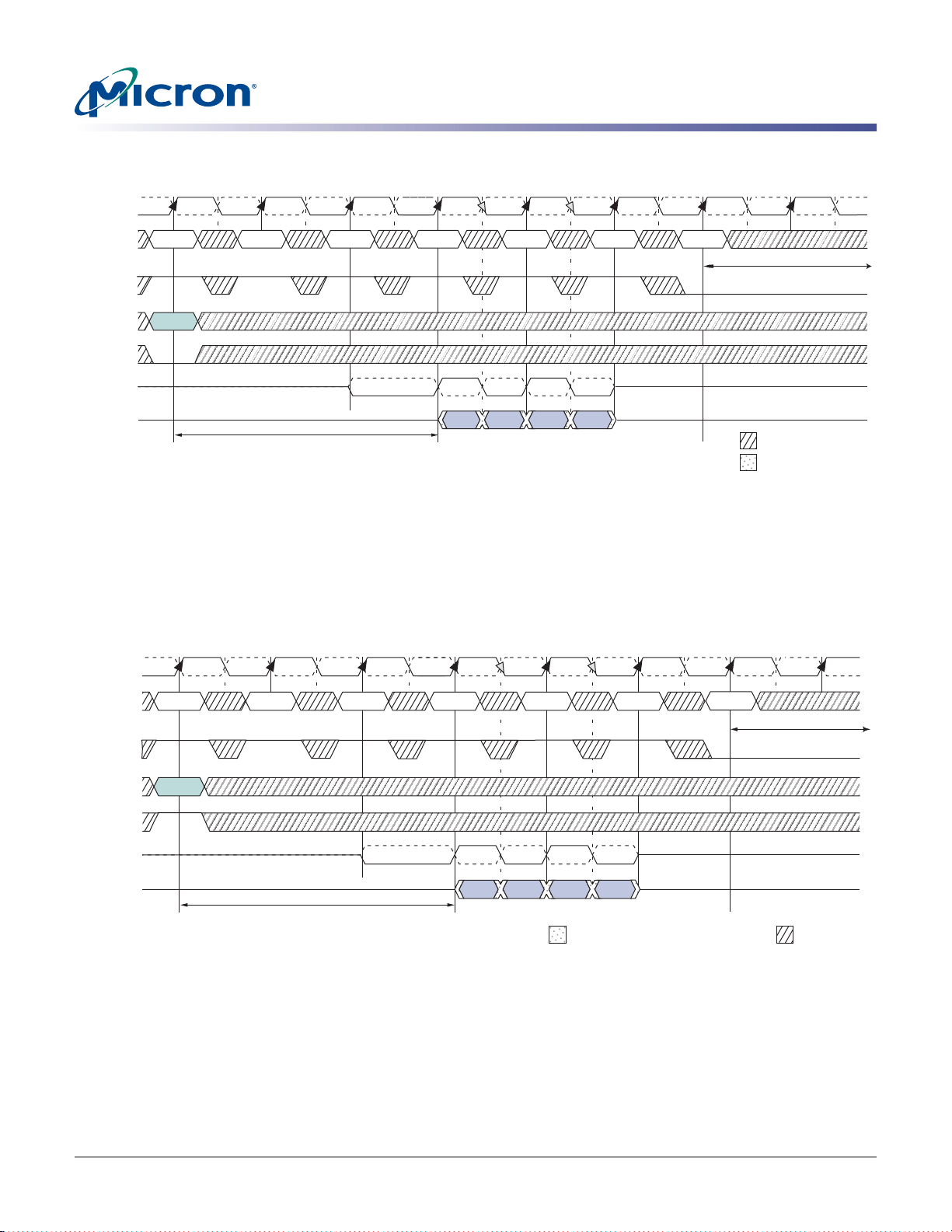
Figure 46: READ to Power-Down or Self Refresh Entry
512Mb: x4, x8, x16 DDR2 SDRAM
Power-Down Mode
CK#
CK
COMMAND
CKE
ADDRESS
A10
DQS, DQS#
DQ
T0 T1 T2
READ
VALID
NOP NOP
RL = 3
NOP
T3 T4 T5
VALID
DOUT
VALID
OUTDOUT DOUT
D
Power-down
or self refresh
Notes: 1. Power-down or self refresh entry may occur after the READ burst completes.
2. In the example shown, READ burst completes at T5; earliest power-down or self refresh
entry is at T6.
Figure 47: READ with Auto Precharge to Power-Down or Self Refresh Entry
T6 T7
2
NOP
1
entry
t
CKE (MIN)
DON’T CARE
TRANSITIONING DATA
CK#
CK
COMMAND
CKE
ADDRESS
A10
DQS, DQS#
DQ
T0 T1 T2
READ
VALID
NOP NOP
RL = 3
NOP
T3 T4 T5
VALID VALID
DOUT DOUTDOUT DOUT
TRANSITIONING DATA
or self refresh
Notes: 1. Power-down or self refresh entry may occur after the READ burst completes.
2. In the example shown, READ burst completes at T5; earliest power-down or self refresh
entry is at T6.
T6 T7
2
NOP
Power-down
entry
1
t
CKE (MIN)
DON’T CARE
PDF: 09005aef8117c18e, Source: 09005aef8211b2e6 Micron Technology, Inc., reserves the right to change products or specifications without notice.
512MbDDR2_2.fm - R ev. K 8/06 EN
67 ©2004 Micron Technology, Inc. All rights reserved.
Page 68
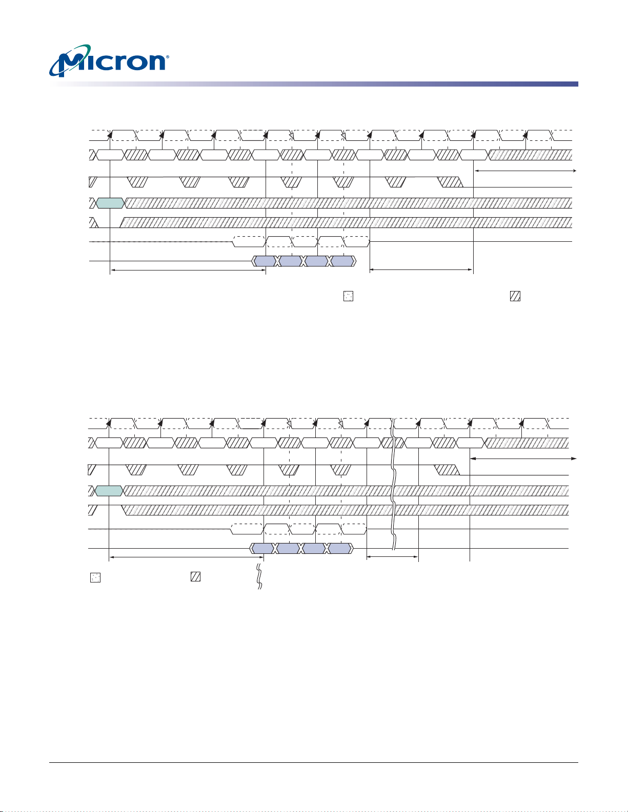
Figure 48: WRITE to Power-Down or Self-Refresh Entry
512Mb: x4, x8, x16 DDR2 SDRAM
Power-Down Mode
CK#
CK
COMMAND
CKE
ADDRESS
A10
DQS, DQS#
DQ
T0 T1 T2
WRITE
VALID
NOP NOP
WL = 3
NOP
T3 T4 T5
VALID VALID
DOUT
DOUT DOUT DOUT
T6
VALID
t
WTR
Notes: 1. Power-down or self refresh entry may occur after the WRITE burst completes.
Figure 49: WRITE with Auto Precharge to Power-Down or Self Refresh Entry
CK#
CK
COMMAND
CKE
T0 T1 T2
WRITE
NOP NOP
NOP
T3 T4 T5
VALID VALID
Ta0
VALID
2
T7 T8
1
NOP
Power-down
or self refresh
1
entry
Ta1 Ta2
NOP
t
CKE (MIN)
DON’T CARETRANSITIONING DATA
t
CKE (MIN)
ADDRESS
DQS, DQS#
PDF: 09005aef8117c18e, Source: 09005aef8211b2e6 Micron Technology, Inc., reserves the right to change products or specifications without notice.
512MbDDR2_2.fm - R ev. K 8/06 EN
VALID
A10
DQ
TRANSITIONING DATA
D
OUT
D
WL = 3
DON’T CARE
Notes: 1. WR is programmed through MR[9, 10, 11] and represents (tWR [MIN] ns / tCK) rounded up
to next integer
2. Internal PRECHARGE occurs at Ta0 when WR has completed; power-down entry may occur
t
CK later at Ta1, prior to tRP being satisfied.
1 x
t
OUTDOUTDOUT
Indicates a break in
time scale
CK.
WR
1
Power-down
or self refresh
entry
68 ©2004 Micron Technology, Inc. All rights reserved.
Page 69
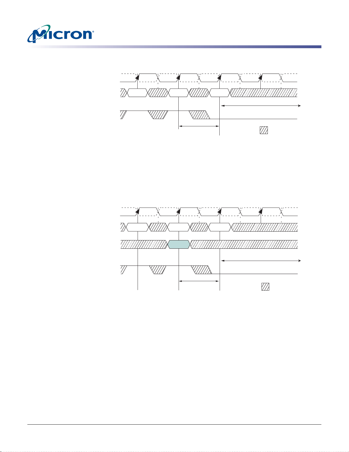
Figure 50: REFRESH Command to Power-Down Entry
512Mb: x4, x8, x16 DDR2 SDRAM
Power-Down Mode
CK#
T0 T1
CK
COMMAND
VALID
REFRESH
CKE
Notes: 1. The earliest precharge power-down entry may occur is at T2 which is 1 x tCK after the
REFRESH command. Precharge power down entry occurs prior to
Figure 51: ACTIVE Command to Power-Down Entry
CK#
CK
COMMAND
T0 T1
VALID
ACTIVE
1 x tCK
T2 T3
NOP
Power-down
1
entry
T2
NOP
t
CKE (MIN)
DON’T CARE
t
RFC (MIN) being satisfied.
T3
ADDRESS
VALID
t
CKE (MIN)
CKE
1 tCK
Power-down
1
DON’T CARE
entry
Notes: 1. The earliest active power-down entry may occur is at T2, which is 1 x tCK after the ACTIVE
command. Active power-down entry occurs prior to tRCD (MIN) being satisfied.
PDF: 09005aef8117c18e, Source: 09005aef8211b2e6 Micron Technology, Inc., reserves the right to change products or specifications without notice.
512MbDDR2_2.fm - R ev. K 8/06 EN
69 ©2004 Micron Technology, Inc. All rights reserved.
Page 70
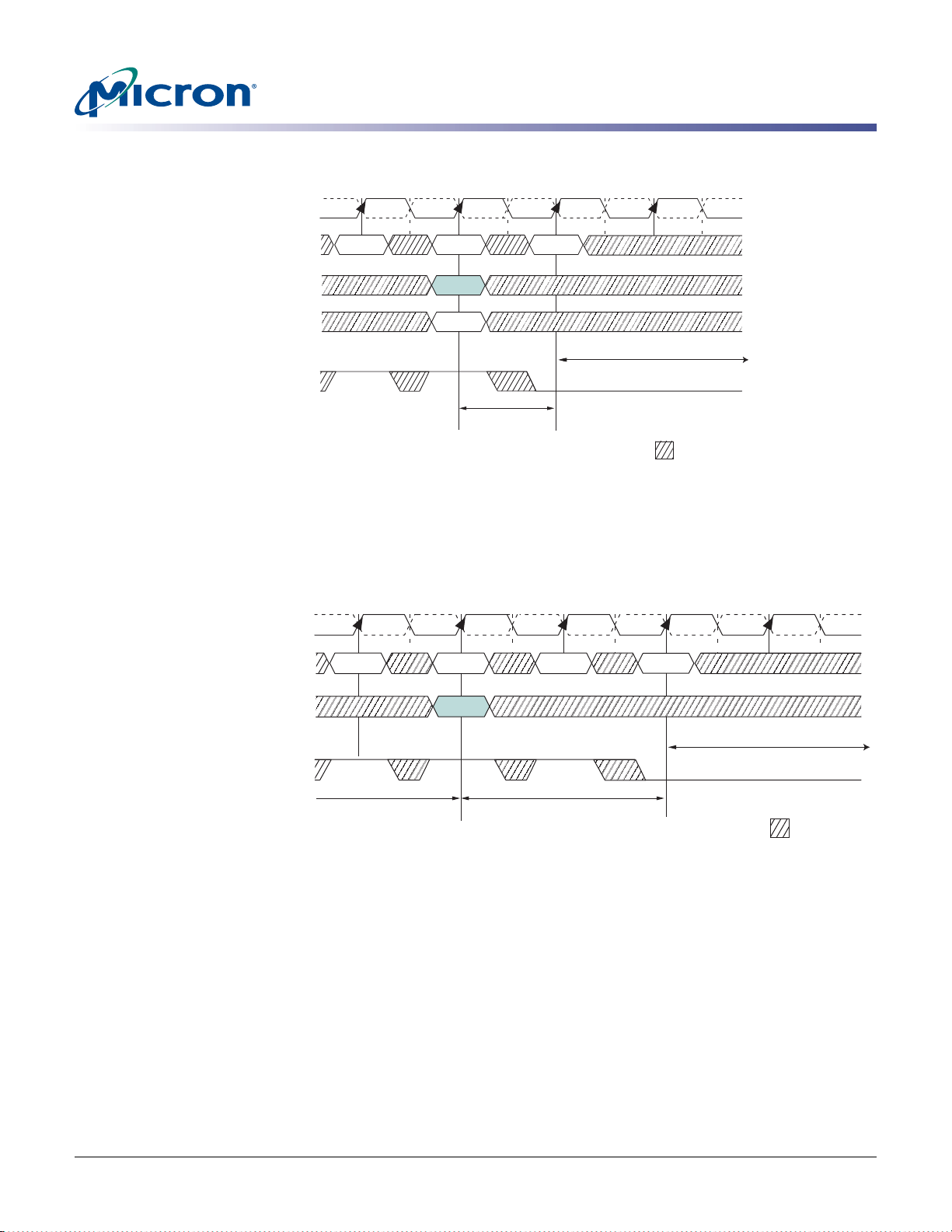
Figure 52: PRECHARGE Command to Power-Down Entry
512Mb: x4, x8, x16 DDR2 SDRAM
Power-Down Mode
CK#
T0 T1
CK
COMMAND
ADDRESS
A10
VALID
PRECHARGE
VALID
ALL BANKS
vs
SINGLE BANK
CKE
1 x tCK
Power-down
entry
Notes: 1. The earliest precharge power-down entry may occur is at T2, which is 1 x tCK after the PRE-
CHARGE command. Precharge power-down entry occurs prior to tRP (MIN) being satisfied.
Figure 53: LOAD MODE Command to Power-Down Entry
CK#
CK
COMMAND
T0 T1
VALID LM
T2
NOP
T2
NOP
T3
t
CKE (MIN)
1
DON’T CARE
T3 T4
NOP
3
ADDRESS
CKE
tRP2
VALID
t
MRD
Power-down
entry
t
CKE (MIN)
1
DON’T CARE
Notes: 1. The earliest precharge power-down entry is at T3, which is after tMRD is satisfied.
2. All banks must be in the precharged state and
t
RP met prior to issuing LM command.
3. Valid address for LM command includes MR, EMR, EMR(2), and EMR(3) registers.
PDF: 09005aef8117c18e, Source: 09005aef8211b2e6 Micron Technology, Inc., reserves the right to change products or specifications without notice.
512MbDDR2_2.fm - R ev. K 8/06 EN
70 ©2004 Micron Technology, Inc. All rights reserved.
Page 71
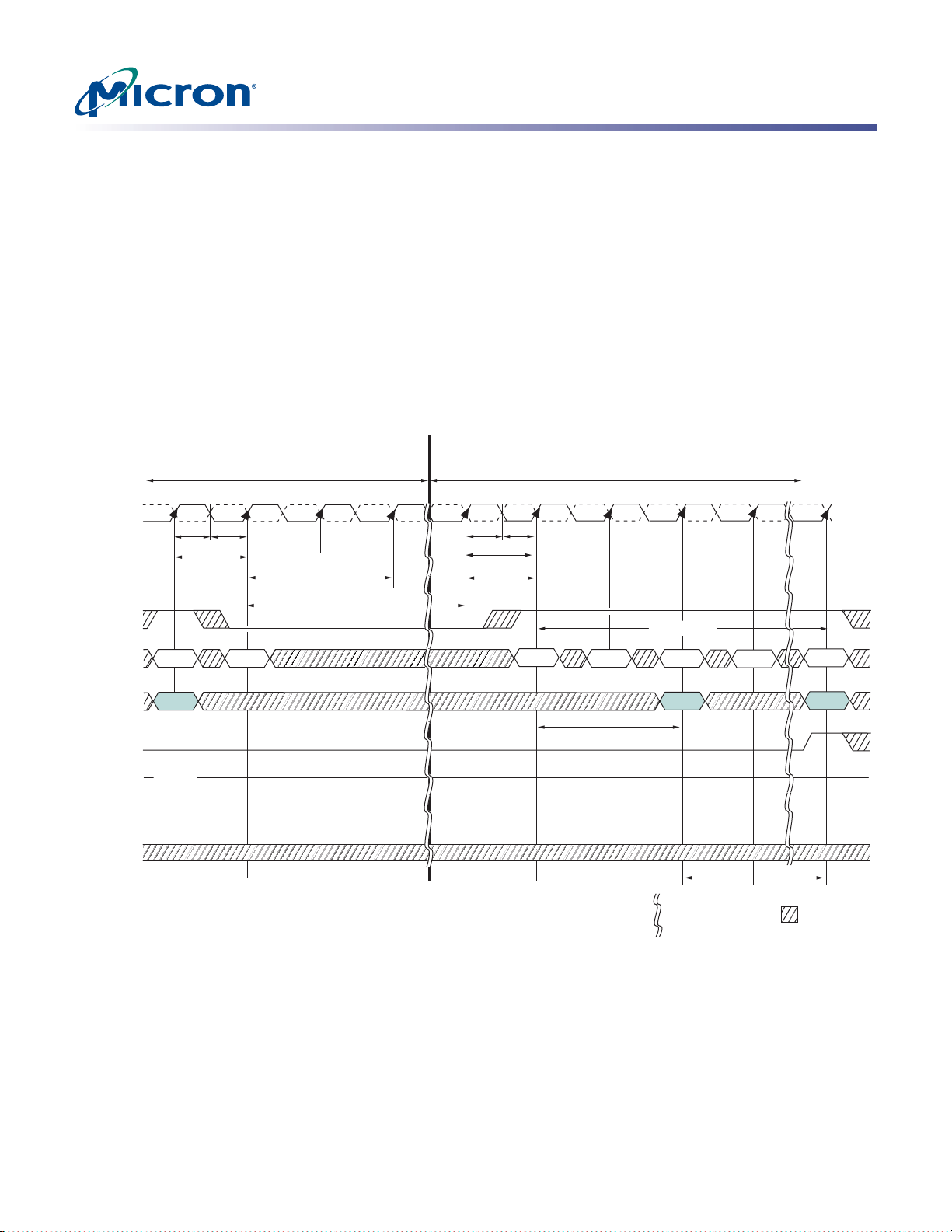
512Mb: x4, x8, x16 DDR2 SDRAM
Precharge Power-Down Clock Frequency Change
Precharge Power-Down Clock Frequency Change
When the DDR2 SDRAM is in precharge power-down mode, ODT must be turned off
and CKE must be at a logic LOW level. A minimum of two differential clock cycles must
pass after CKE goes LOW before clock frequency may change. The device input clock
frequency is allowed to change only within minimum and maximum operating frequencies specified for the particular speed grade. During input clock frequency change, ODT
and CKE must be held at stable LOW levels. Once the input clock frequency is changed,
new stable clocks must be provided to the device before precharge power-down may be
exited, and DLL must be reset via EMR after precharge power-down exit. Depending on
the new clock frequency , an additional LM command might be r equired to appropriately
set the WR MR[11, 10, 9]. During the DLL relock period of 200 cycles, ODT must remain
off. After the DLL lock time, the DRAM is ready to operate with a new clock frequency.
Figure 54: Input Clock Frequency Change During Precharge Power-Down Mode
PREVIOUS CLOCK FREQUENCY NEW CLOCK FREQUENCY
CK#
CK
T0 T1 T3 Ta0T2
t
CHtCL
t
CK
x t
2
CK (MIN)
t
CHtCL
2
1 x tCK (MIN)
Ta1 Ta2 Tb0Ta3
t
CK
3
Ta4
CKE
COMMAND
ADDR
ODT
DQS, DQS#
DQ
DM
VALID
VALID
High-Z
High-Z
1
NOP
Enter precharge
power-down mode
t
CKE (MIN)
4
Frequency
change
NOP
Exit precharge
power-down mode
NOP
t
XP
t
CKE (MIN)
4
LM
DLL RESET
Indicates a break in
time scale
200 x tCK
Notes: 1. If this command is a PRECHARGE (or if the device is already in the idle state), then the
power-down mode shown is precharge power-down, which is required prior to the clock
frequency change.
2. A minimum of 2 x tCK is required after entering precharge power-down prior to changing
clock frequencies.
3. Once the new clock frequency has changed and is stable, a minimum of 1 x
prior to exiting precharge power-down.
t
4. Minimum CKE HIGH time is
CKE = 3 x tCK. Minimum CKE LOW time is tCKE = 3 x tCK. This
requires a minimum of three clock cycles of registration.
NOP
t
CK is required
VALID
VALID
DON’T CARE
PDF: 09005aef8117c18e, Source: 09005aef8211b2e6 Micron Technology, Inc., reserves the right to change products or specifications without notice.
512MbDDR2_2.fm - R ev. K 8/06 EN
71 ©2004 Micron Technology, Inc. All rights reserved.
Page 72

RESET Function
(CKE LOW Anytime)
512Mb: x4, x8, x16 DDR2 SDRAM
RESET Function
DDR2 SDRAM applications may go into a reset state anytime during normal operation.
If an application enters a reset condition, CKE is used to ensure the DDR2 SDRAM
device resumes normal operation after re-initializing. All data will be lost during a reset
condition; however, the DDR2 SDRAM device will continue to operate properly if the
following conditions outlined in this section are satisfied.
The reset condition defined here assumes all supply voltages (V
V
REF) are stable and meet all DC specifications prior to, during, and after the RESET
DD, VDDQ, VDDL, and
operation. All other input pins of the DDR2 SDRAM device are a “Don’t Care” during
RESET with the exception of CKE.
If CKE asynchronously drops LOW during any valid operation (including a READ or
WRITE burst), the memory controller must satisfy the timing parameter
t
DELAY before
turning off the clocks. Stable cl ocks must exist at the CK, CK# inputs of the DRAM before
CKE is raised HIGH, at which time the normal initialization sequence must occur. See
“Initialization” on page 16. The DDR2 SDRAM device is now ready for normal operation
after the initialization sequence. Figure55 on page 73 shows the proper sequence for a
RESET operation.
PDF: 09005aef8117c18e, Source: 09005aef8211b2e6 Micron Technology, Inc., reserves the right to change products or specifications without notice.
512MbDDR2_2.fm - R ev. K 8/06 EN
72 ©2004 Micron Technology, Inc. All rights reserved.
Page 73
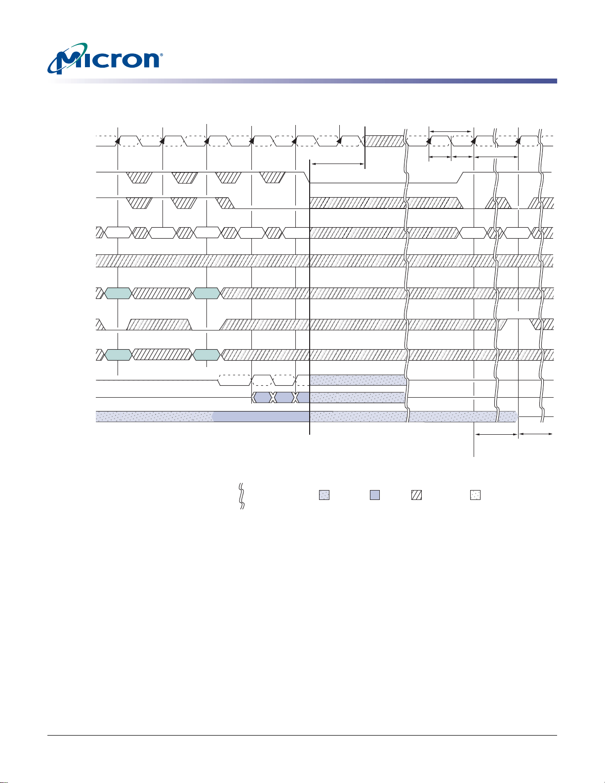
Figure 55: RESET Function
512Mb: x4, x8, x16 DDR2 SDRAM
RESET Function
CK#
CKE
ODT
COMMAND
DM
ADDRESS
A10
BA0, BA1
DQS
DQ
R
CK
T0 T1 T2
2
READ
3
Col n
Bank a
3
3
TT
High-Z
High-Z
NOP
1
READ
Col n
Bank b
T3 T4 T5
t
DELAY
NOP
1
D
OUT
1
NOP
D
OUT
D
OUT
Ta0
t
CK
t
t
CL
6
High-Z
High-Z
CL
NOP
t
1
5
Tb0
CKE (MIN)
PRE
ALL BANKS
High-Z
System
RESET
Indicates a break in
time scale
Unknown RTT ON
Notes: 1. Either NOP or DESELECT command may be applied.
2. PRE = PRECHARGE command.
3. DM represents DM for x4/x8 configuration and UDM, LDM for x16 configuration. DQS represents DQS, DQS#, UDQS, UDQS #, LDQS, LDQS#, RDQS, RDQS# for the appropriate configuration (x4, x8, x16).
4. Initialization timing is shown in Figure 7 on page 16.
5. In certain cases where a READ cycle is interrupted, CKE going HIGH may result in the completion of the burst.
6. V
DD, VDDL, VDDQ, VTT, and VREF must be valid at all times.
t
T = 400ns (MIN)
Start of normal
initialization
sequence
DON’T CARE TRANSITIONING DATA
4
RP
A
PDF: 09005aef8117c18e, Source: 09005aef8211b2e6 Micron Technology, Inc., reserves the right to change products or specifications without notice.
512MbDDR2_2.fm - R ev. K 8/06 EN
73 ©2004 Micron Technology, Inc. All rights reserved.
Page 74

ODT Timing
512Mb: x4, x8, x16 DDR2 SDRAM
ODT Timing
Once a 12ns delay (tMOD) has been satisfied, and after the ODT function has been
enabled via the EMR LOAD MODE command, ODT can be accessed under two timing
categories. ODT will operate in either synchronous mode or asynchronous mode,
depending on the state of CKE. ODT can switch anytime except during self refr esh mode
and a few clocks after being enabled via EMR, as shown in Figure56 on page 75.
There are two timing categories for ODT—turn-on and turn-off. During active mode
(CKE HIGH) and fast-exit power-down mode (any row of any bank open, CKE LOW,
MR[12 = 0]),
Figure58 on page 76 and Table12 on page 76.
During slow-exit power-down mode (any row of any bank open, CKE LOW, MR[12] = 1)
and precharge power-down mode (all banks/rows precharged and idle, CKE LOW),
t
AONPD and tAOFPD timing paramete rs are applied, as shown in Figure59 on page 77
and Table 13 on page 77.
t
AOND, tAON, tAOFD, and tAOF timing parameters are applied, as shown in
ODT turn-off timing, prior to entering any power-down mode, is determined by the
parameter
signal satisfies
(MIN) is satisfied,
shows the example where
until state T3. When
t
ANPD (MIN), as shown in Figure 60 on page 78. At state T2, the ODT HIGH
t
ANPD (MIN) prior to entering power-down mode at T5. When tANPD
t
AOFD and tAOF timing parameters apply. Figure 60 on page78 also
t
ANPD (MIN) is not satisfied since ODT HIGH does not occur
t
ANPD (MIN) is not satisfied, tAOFPD timing parameters apply.
ODT turn-on timing prior to entering any power-down mode is determined by the
parameter
satisfies
satisfied,
where
t
ANPD (MIN) is not satisfied, tAONPD timing parameters apply.
t
ANPD, as shown in Figure61 on page 79. At state T2, the ODT HIGH signal
t
ANPD (MIN) prior to entering power-down mode at T5. When tANPD (MIN) is
t
AOND and tAON timing parameters apply. Figure61 also shows the example
t
ANPD (MIN) is not satisfied since ODT HIGH does not occur until state T3. When
ODT turn-off timing after exiting any power-down mode is d etermined b y the par ameter
t
AXPD (MIN), as shown in Figure62 on page 80. At state Ta1, the ODT LOW signal satis-
t
fies
AXPD (MIN) after exiting power-do wn mode at state T1. When tAXPD (MIN) is satis-
t
fied,
AOFD and tAOF timing parameters apply. Figure62 also shows the example where
t
AXPD (MIN) is not satisfied since ODT LOW occurs at state Ta0. When tAXPD (MIN) is
not satisfied,
ODT turn-on timing after exiting either slow-exit powe r-down mode or precharge
power-down mode is determined by the parameter
on page 81. At state Ta1, the ODT HIGH signal satisfies
down mode at state T1. When
eters apply. Figure63 also shows the example where
ODT HIGH occurs at state Ta0. When
t
AOFPD timing parameters apply.
t
AXPD (MIN) is satisfied, tAOND and tAON timing param-
t
AXPD (MIN) is not satisfied, tAONPD timing
t
AXPD (MIN), as shown in Figure 63
t
AXPD (MIN) after exiting power-
t
AXPD (MIN) is not satisfied since
parameters apply.
PDF: 09005aef8117c18e, Source: 09005aef8211b2e6 Micron Technology, Inc., reserves the right to change products or specifications without notice.
512MbDDR2_2.fm - R ev. K 8/06 EN
74 ©2004 Micron Technology, Inc. All rights reserved.
Page 75
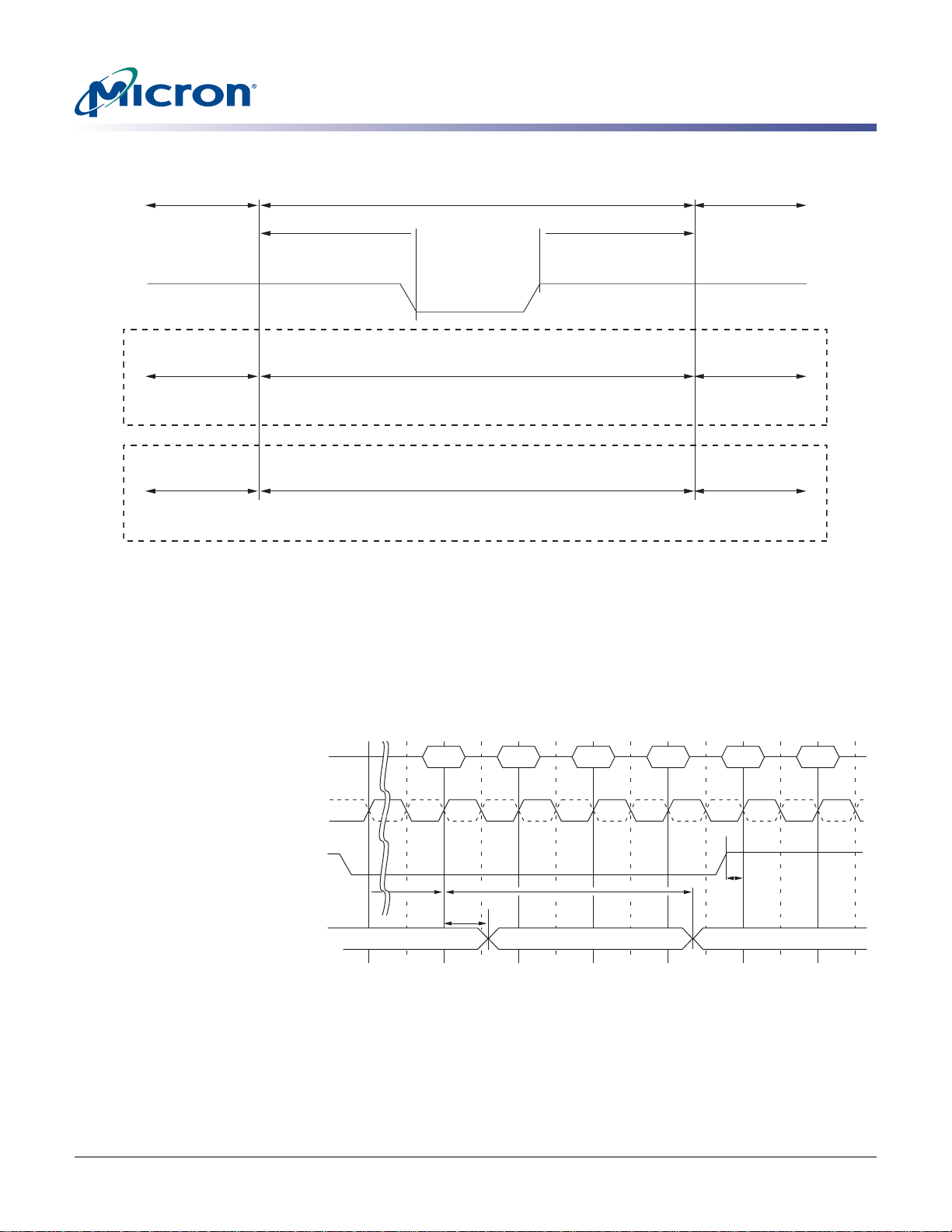
512Mb: x4, x8, x16 DDR2 SDRAM
Figure 56: ODT Timing for Entering and Exiting Power-Down Mode
ODT Timing
Synchronous
t
ANPD (3 tCKs)
st
1
CKE latched LOW
CKE
Any mode except
self refresh mode
Applicable modes
t
AOND/tAOFD
Applicable timing parameters
Active power-down fast (synchronous)
Active power-down slow (asynchronous)
Precharge power-down (asynchronous)
t
AOND/tAOFD (synchronous)
t
AONPD/tAOFPD (asynchronous)
MRS Command to ODT Update Delay
Asynchronous
t
AXPD (8 tCKs)
st
1
CKE latched HIGH
SynchronousSynchronous or
Any mode except
self refresh mode
t
AOND/tAOFD
During normal operation, the value of the effective termination resistance can be
changed with an EMRS set command.
t
MOD (MAX) updates the RTT setting.
Figure 57: Timing for MRS Command to ODT Update Delay
1
CMD
EMRS
CK#
CK
2
ODT
t
AOFD
0ns
Internal
TT Setting
R
Old Setting Undefined New Setting
Notes: 1. LM command directed to mode register, which updates the information in EMR(1)[A6, A2],
TT (nominal).
i.e., R
2. To prevent any impedance glitch on the channel, the following conditions must be met:
t
AOFD must be met before issuing the LM command; ODT must remain LOW for the entire
duration of the
t
MOD window, until tMOD is met.
NOP NOPNOP NOP NOP
t
MOD
2
t
IS
PDF: 09005aef8117c18e, Source: 09005aef8211b2e6 Micron Technology, Inc., reserves the right to change products or specifications without notice.
512MbDDR2_2.fm - R ev. K 8/06 EN
75 ©2004 Micron Technology, Inc. All rights reserved.
Page 76
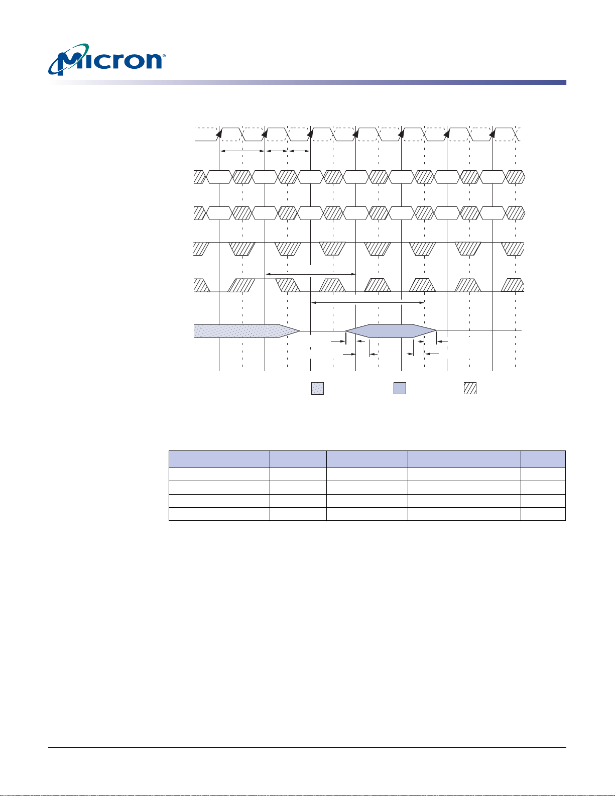
512Mb: x4, x8, x16 DDR2 SDRAM
Figure 58: ODT Timing for Active or Fast-Exit Power-Down Mode
CK#
CK
T1T0 T2 T3 T4 T5 T6
t
CK
t
t
CL
CH
ODT Timing
CMD
ADDR
CKE
ODT
R
TT
VALIDVALID VALID VALIDVALID VALID
VALIDVALID VALID VALIDVALID VALID VALID
t
AOND
t
AOFD
t
AON (MIN)
t
AON (MAX)
RTT Unknown
TT
On
R
t
AOF (MAX)
t
AOF (MIN)
Table 12: DDR2-400/533 ODT Timing for Active and Fast-Exit Power-Down Modes
Parameter Symbol Min Max Units
t
ODT turn-on delay
ODT turn-on
ODT turn-off delay
ODT turn-off
AOND 2 2
t
AON
t
AOFD 2.5 2.5
t
AOF
t
AC (MIN)
t
AC (MIN)
t
AC (MAX) + 1,000 ps
t
AC (MAX) + 600 ps
VALID
DON’T CARE
t
t
CK
CK
Note: The half-clock of tAOFD’s 2.5 tCK assumes a 50/50 clock duty cycle. This half-clock value
must be derated by the amount of half-clock duty cycle error. For example, if the clock
duty cycle was 47/53,
0.03, or 2.53, for
PDF: 09005aef8117c18e, Source: 09005aef8211b2e6 Micron Technology, Inc., reserves the right to change products or specifications without notice.
512MbDDR2_2.fm - R ev. K 8/06 EN
t
AOFD would actually be 2.5 - 0.03, or 2.47, for tAOF (MIN) and 2.5 +
t
AOF (MAX).
76 ©2004 Micron Technology, Inc. All rights reserved.
Page 77
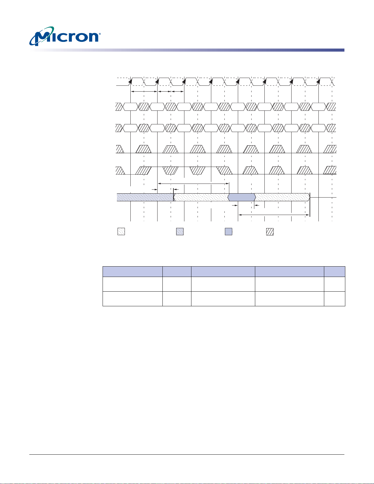
512Mb: x4, x8, x16 DDR2 SDRAM
Figure 59: ODT Timing for Slow-Exit or Precharge Power-Down Modes
ODT Timing
CK#
CK
CMD
ADDR
CKE
ODT
R
TT
t
CK
t
AONPD (MIN)
Transitioning R
T1T0 T2 T3 T4 T5 T6
t
t
CL
CH
VALIDVALID VALID VALIDVALID VALID
VALIDVALID VALID VALIDVALID VALID VALID
t
AONPD (MAX)
t
AOFPD (MIN)
TT
RTT Unknown
RTT On
t
AOFPD (MAX)
VALID
DON’T CARE
T7
VALID
VALID
Table 13: DDR2-400/533 ODT Timing for Slow-Exit and Precharge Power-Down Modes
Parameter Symbol Min Max Units
ODT turn-on
(power-down mode)
ODT turn-off
(power-down mode)
t
AONPD
t
AOFPD
t
AC (MIN) + 2,000 2 x tCK +tAC (MAX) +
1,000
t
AC (MIN) + 2,000 2.5 x tCK + tAC (MAX) +
1,000
ps
ps
PDF: 09005aef8117c18e, Source: 09005aef8211b2e6 Micron Technology, Inc., reserves the right to change products or specifications without notice.
512MbDDR2_2.fm - R ev. K 8/06 EN
77 ©2004 Micron Technology, Inc. All rights reserved.
Page 78
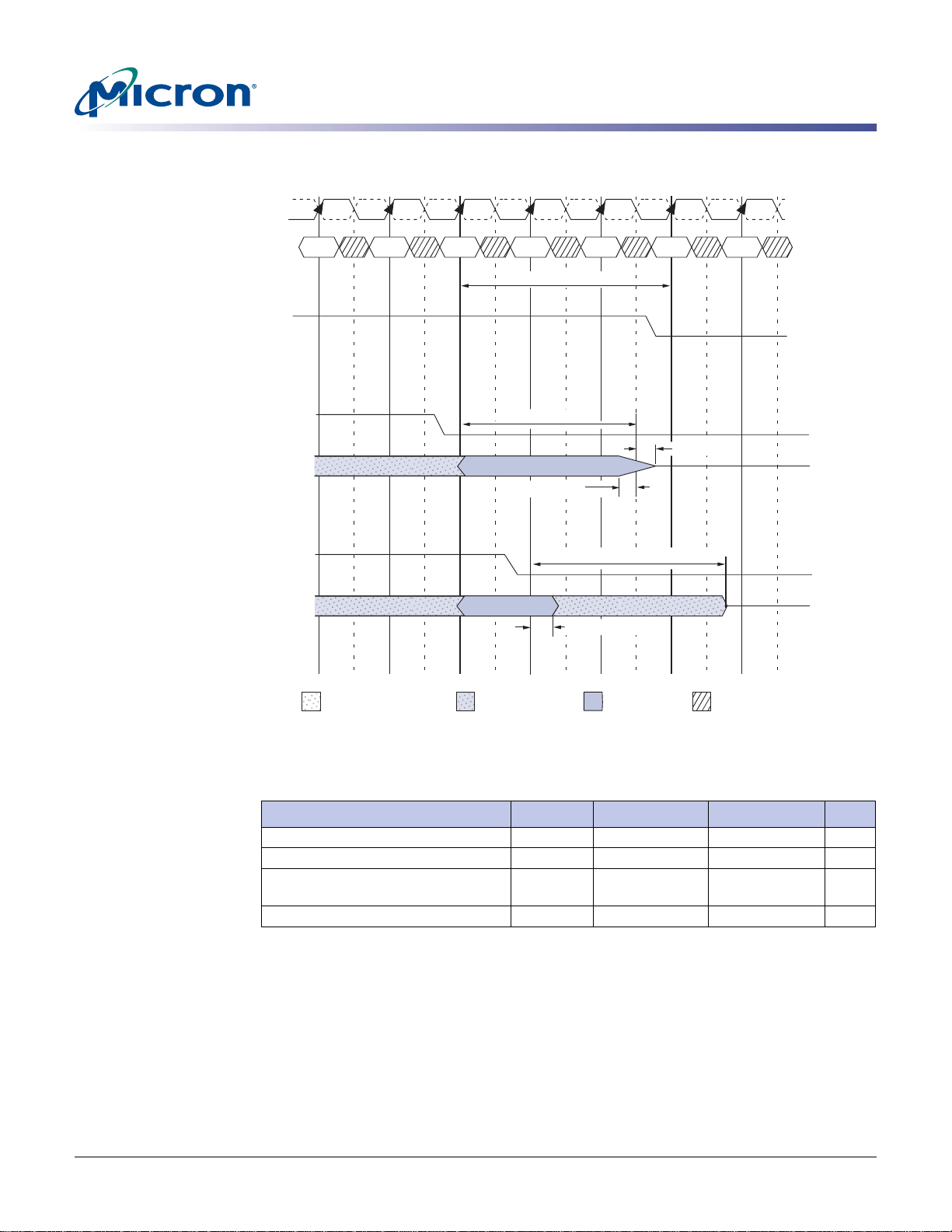
512Mb: x4, x8, x16 DDR2 SDRAM
Figure 60: OD T Turn-off Timings when Entering Power-Down Mode
CK#
CK
T1T0 T2 T3 T4 T5 T6
ODT Timing
CKE
ODT
RTT
ODT
RTT
NOPNOP NOP NOPNOP NOP
t
ANPD (MIN)
t
AOFD
t
AOF (MIN)
t
AOFPD (MAX)
t
AOFPD (MIN)
t
AOF (MAX)
NOP
Transitioning RTT
RTT Unknown RTT On
DON’T CARE
Table 14: DDR2-400/533 ODT Turn-off Timings when Entering Power-Down Mode
Parameter Symbol Min Max Units
t
ODT turn-off delay
ODT turn-off
ODT turn-off
(power-down mode)
ODT to power-down entry latency
Note: The half-clock of tAOFD’s 2.5 tCK assumes a 50/50 clock duty cycle. This half-clock value
must be derated by the amount of half-clock duty cycle error. For example, if the clock
duty cycle was 47/53,
0.03, or 2.53, for
t
AOFD would actually be 2.5 - 0.03, or 2.47, for tAOF (MIN) and 2.5 +
t
AOF (MAX).
AOFD 2.5 2.5
t
AOF
t
AOFPD
t
ANPD 3
t
AC (MIN)
t
AC (MIN) +
2,000
t
AC (MAX) + 600 ps
2.5 x tCK + tAC
(MAX) + 1,000
t
t
CK
ps
CK
PDF: 09005aef8117c18e, Source: 09005aef8211b2e6 Micron Technology, Inc., reserves the right to change products or specifications without notice.
512MbDDR2_2.fm - R ev. K 8/06 EN
78 ©2004 Micron Technology, Inc. All rights reserved.
Page 79
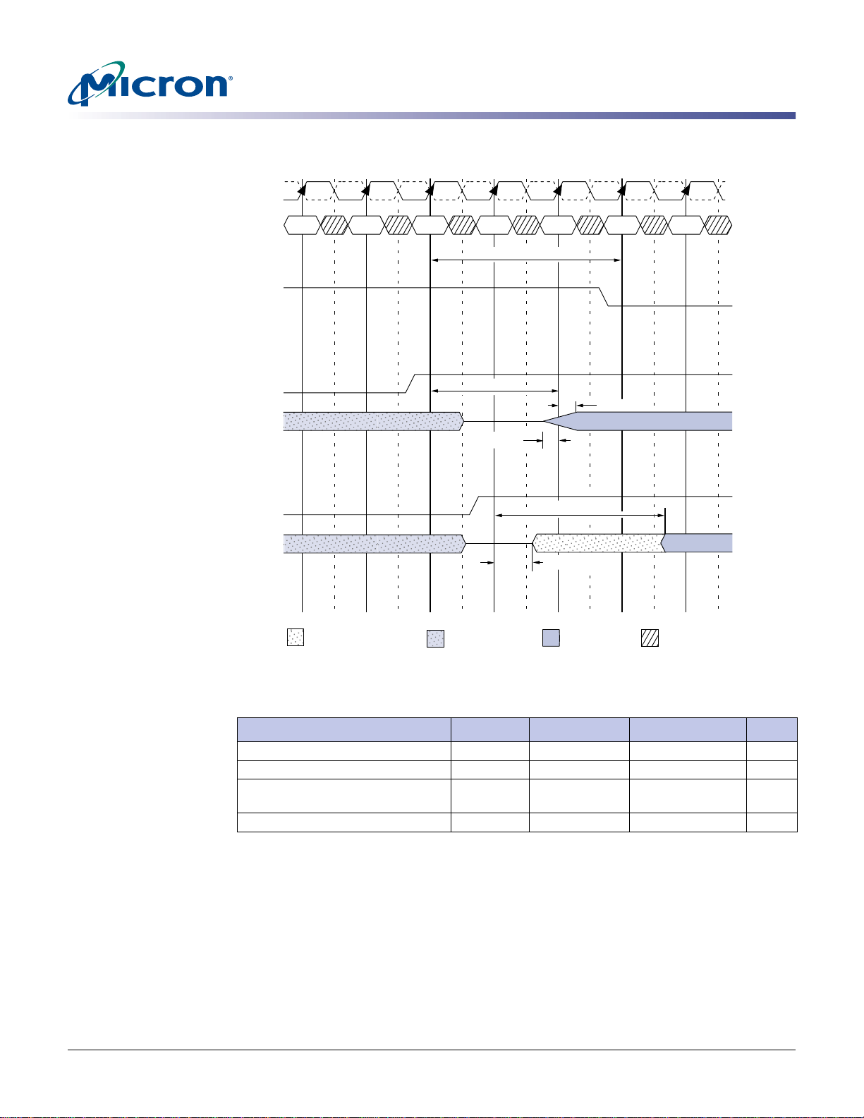
512Mb: x4, x8, x16 DDR2 SDRAM
Figure 61: ODT Turn-On Timing when Entering Power-Down Mode
CK#
CK
T1T0 T2 T3 T4 T5 T6
ODT Timing
CKE
ODT
RTT
ODT
RTT
NOPNOP NOP NOPNOP NOP
t
ANPD (MIN)
t
AOND
t
AON (MAX)
t
AON (MIN)
t
AONPD (MAX)
t
AONPD (MIN)
NOP
Transitioning RTT
RTT Unknown
R
TT On
Table 15: DDR2-400/533 ODT Turn-on Timing when Entering Power-Down Mode
Parameter Symbol Min Max Units
t
ODT turn-on delay
ODT turn-on
ODT turn-on
(power-down mode)
ODT to power-down entry latency
AOND 2 2
t
AON
t
AONPD
t
ANPD 3
t
AC (MIN)
t
AC (MIN) +
2,000
t
AC (MAX) + 1,000 ps
(MAX) + 1,000
DON’T CARE
2 x tCK + tAC
t
t
CK
ps
CK
PDF: 09005aef8117c18e, Source: 09005aef8211b2e6 Micron Technology, Inc., reserves the right to change products or specifications without notice.
512MbDDR2_2.fm - R ev. K 8/06 EN
79 ©2004 Micron Technology, Inc. All rights reserved.
Page 80
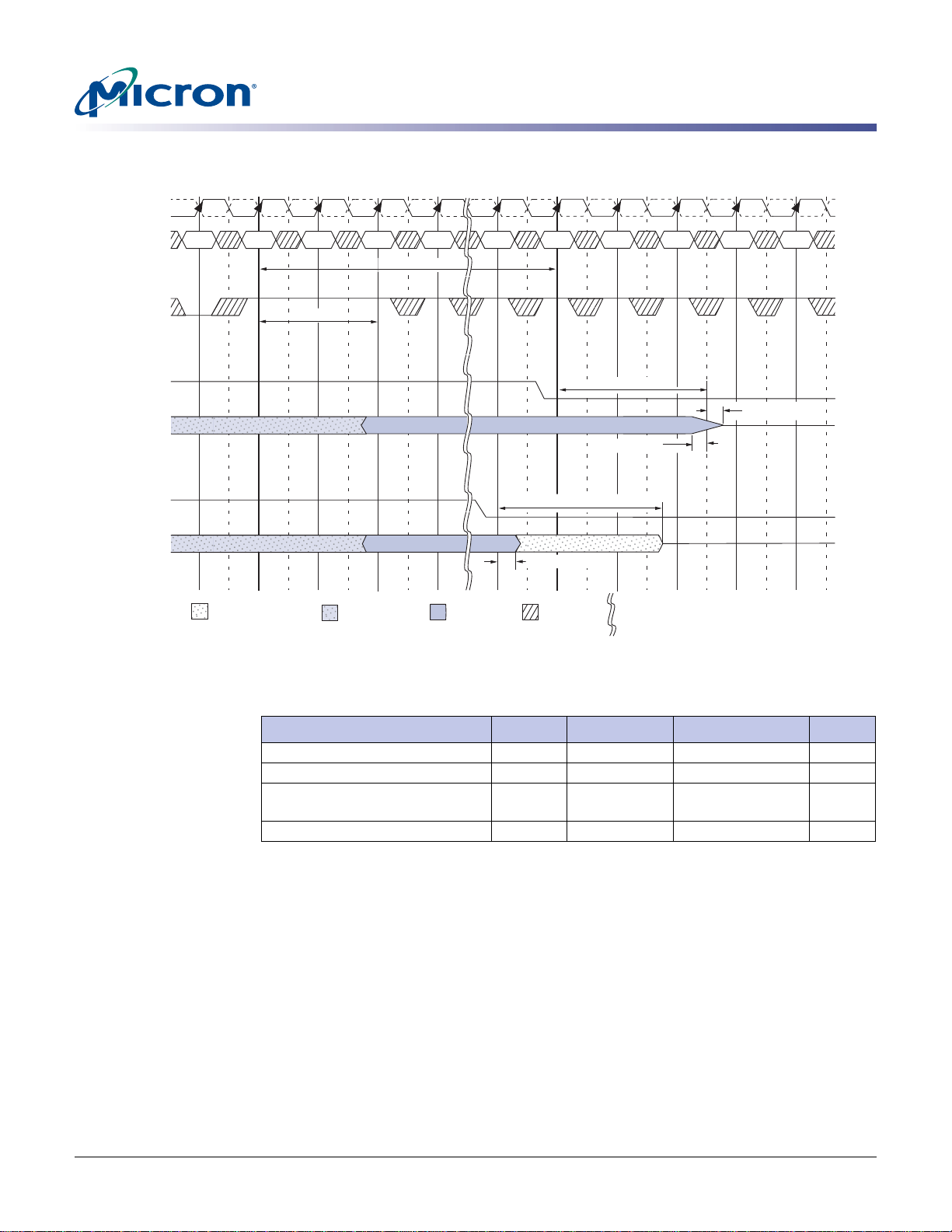
512Mb: x4, x8, x16 DDR2 SDRAM
Figure 62: ODT Turn-Off Timing when Exiting Power-Down Mode
CK#
CK
COMMAND
T1T0 T2 T3 T4 Ta0 Ta1
NOPNOP NOP NOPNOP NOP NOP
t
AXPD (MIN)
ODT Timing
Ta2 Ta3 Ta4 Ta5
NOPNOP NOP
NOP
CKE
ODT
RTT
ODT
RTT
Transitioning RTT
t
CKE (MIN)
RTT Unknown
RTT On
t
AOFPD (MAX)
t
AOFPD (MIN)
DON’T CARE
t
AOFD
t
AOF (MIN)
Indicates a break in
time scale
Table 16: DDR2-400/533 ODT Turn-off Timing when Exiting Power-Down Mode
Parameter Symbol Min Max Units
t
ODT turn-off delay
ODT turn-off
ODT turn-off
(power-down mode)
ODT to power-down exit latency
AOFD 2.5 2.5
t
AOF
t
AOFPD
t
AXPD 8
t
AC (MIN)
t
AC (MIN) +
2,000
t
AC (MAX) + 600 ps
2.5 x tCK + tAC
(MAX) + 1,000
t
AOF (MAX)
t
t
CK
ps
CK
Note: The half-clock of tAOFD’s 2.5 tCK assumes a 50/50 clock duty cycle. This half-clock value
must be derated by the amount of half-clock duty cycle error. For example, if the clock
duty cycle was 47/53,
0.03, or 2.53, for
PDF: 09005aef8117c18e, Source: 09005aef8211b2e6 Micron Technology, Inc., reserves the right to change products or specifications without notice.
512MbDDR2_2.fm - R ev. K 8/06 EN
t
AOFD would actually be 2.5 - 0.03, or 2.47, for tAOF (MIN) and 2.5 +
t
AOF (MAX).
80 ©2004 Micron Technology, Inc. All rights reserved.
Page 81
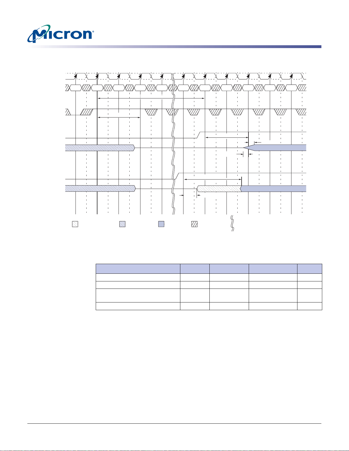
512Mb: x4, x8, x16 DDR2 SDRAM
Figure 63: ODT Turn-on Timing when Exiting Power-Down Mode
CK#
CK
COMMAND
T1T0 T2 T3 T4 Ta0 Ta1
NOPNOP NOP NOPNOP NOP
t
AXPD (MIN)
NOP
ODT Timing
Ta2 Ta3 Ta4 Ta5
NOPNOP NOP
NOP
CKE
ODT
RTT
ODT
RTT
Transitioning RTT RTT Unknown RTT On
t
CKE (MIN)
t
AONPD (MAX)
t
AONPD (MIN)
DON’T CARE
t
AOND
t
AON (MIN)
Indicates a break in
time scale
Table 17: DDR2-400/533 ODT Turn-On Timing when Exiting Power-Down Mode
Parameter Symbol Min Max Units
t
ODT turn-on delay
ODT turn-on
ODT turn-on
(power-down mode)
ODT to power-down exit latency
AOND 2 2
t
AON
t
AONPD
t
AXPD 8
t
AC (MIN)
t
AC (MIN) +
2,000
t
AC (MAX) + 1,000 ps
(MAX) + 1,000
t
AON (MAX)
2 x tCK + tAC
t
t
CK
ps
CK
PDF: 09005aef8117c18e, Source: 09005aef8211b2e6 Micron Technology, Inc., reserves the right to change products or specifications without notice.
512MbDDR2_2.fm - R ev. K 8/06 EN
81 ©2004 Micron Technology, Inc. All rights reserved.
Page 82
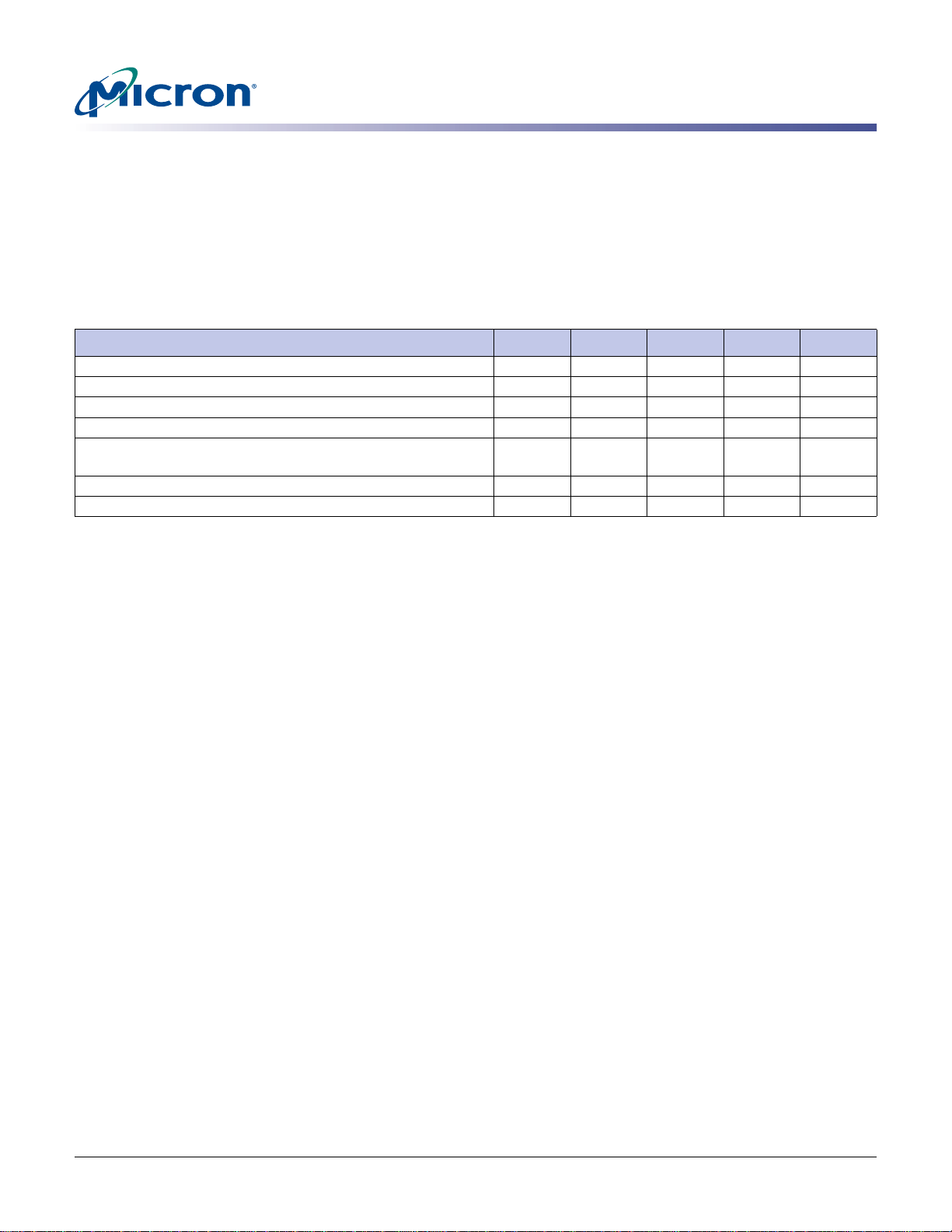
512Mb: x4, x8, x16 DDR2 SDRAM
Absolute Maximum Ratings
Absolute Maximum Ratings
Stresses greater than those listed may cause permanent damage to the device. This is a
stress rating only, and functional operation of the device at these or any other conditions
above those indicated in the operational sections of this specification is not impli e d.
Exposure to absolute maximum rating conditions for extended periods may affect reliability.
Table 17: Absolute Maximum DC Ratings
Parameter Symbol Min Max Units Notes
DD supply voltage relative to VSS
V
DDQ supply voltage relative to VSSQ
V
DDL supply voltage relative to VSSL
V
Voltage on any ball relative to V
Input leakage current; any input 0V ≤ V
not under test = 0V)
Output leakage current; 0V ≤ V
REF leakage current; VREF = Valid VREF le vel
V
Notes: 1. VDD, VDDQ, and VDDL must be within 300mV of each other at all times.
SS
OUT
≤ VDDQ; DQ and ODT disabled
2. V
REF ≤ 0.6 x VDDQ; however, VREF may be ≥ VDDQ provided that VREF ≤ 300mV.
3. Voltage on any I/O may not exceed voltage on V
IN ≤ VDD; all other balls
VDD –1.0 2.3 V 1
VDDQ –0.5 2.3 V 1, 2
VDDL–0.5 2.3 V 1
VIN, V OUT –0.5 2.3 V 3
I
I
VREF
I
OZ
I
–5 5 µA
–5 5 µA
–2 2 µA
DDQ.
Temperature and Thermal Impedance
It is imperative that the DDR2 SDRAM device’s temperature specifications, shown in
Table 18 on page 83, be maintained in order to ensure the junction temperature is in the
proper operating range to meet data sheet s peci fi cations. An important step in maintaining the proper junction temperature is using the device’s thermal impedances
correctly. The thermal impedances are listed in Table 19 on page 83 for the applicable
and available die revision and packages.
Incorrectly using thermal impedances can produce significant errors. Read Micron
Technical Note TN-00-08, “Thermal Applications,” prior to using the thermal impedances listed below. For designs that are expected to last several years and require the
flexibility to use several designs, consider using final target theta values, rather than
existing values, to account for larger thermal impedances.
The DDR2 SDRAM device’s safe junction temperature range can be maintained when
the T
specification is not exceeded. In applications where the device’s ambient temper-
C
ature is too high, use of forced air and/or heat sinks may be required in order to satisfy
the case temperature specifications.
PDF: 09005aef8117c18e, Source: 09005aef8211b2e6 Micron Technology, Inc., reserves the right to change products or specifications without notice.
512MbDDR2_2.fm - R ev. K 8/06 EN
82 ©2004 Micron Technology, Inc. All rights reserved.
Page 83
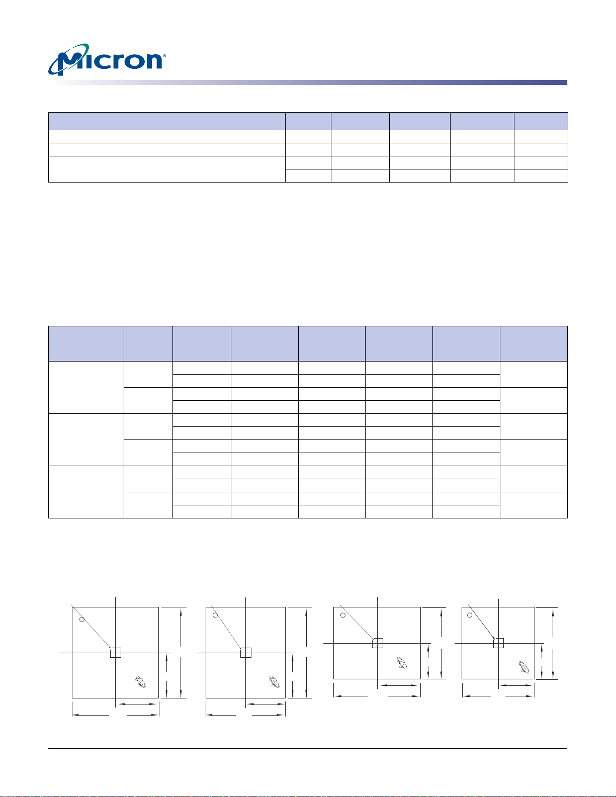
512Mb: x4, x8, x16 DDR2 SDRAM
Temperature and Thermal Impedance
Table 18: Temperature Limits
Parameter Symbol Min Max Units Notes
Storage temperature
Operating temperature – commercial
Operating temperature – industrial
Notes: 1. MAX storage case temperature; T
Figure 64. This case temperature limit is allowed to be exceeded briefly during package
reflow, as noted in Micron technical note, TN-00-15, “Recommended Soldering Parameters.”
2. MAX operating case temperature; TC is measured in the center of the package, as shown in
Figure 64.
3. Device functionality is not guaranteed if the device exceeds maximum T
4. Both temperature specifications must be satisfied.
5. Operating ambient temperature surrounding the package.
Table 19: Thermal Impedance
T
T
STG
T
C
T
C
AMB
–55 100 °C 1
085°C2, 3
–40 95 °C 2, 3, 4
–40 85 °C 4, 5
is measured in the center of the package, as shown in
STG
during operation.
C
Die Rev Package Substrate
1
B
60-ball 2-layer 53.2 40.0 37.2 27.5 2.9
θ JA (°C/W)
Airflow =
0m/s
θ JA (°C/W)
Airflow =
4-layer 37.4 30.9 27.7 24.2
84-ball 2-layer 50.2 36.8 32.1 24.5 3.1
4-layer 34.9 28.0 25.5 21.3
1
C
60-ball 2-layer 56.9 43.6 38.5 30.6 3.8
4-layer 40.6 34.1 31.3 27.0
84-ball 2-layer 56.8 42.8 37.7 24.8 3.9
4-layer 40.3 33.2 30.4 23.5
Last shrink
2
target
60-ball 2-layer 60.0 48.0 45.0 32.0 5.0
4-layer 42.0 36.0 34.0 29.0
84-ball 2-layer 59.0 45.0 40.0 27.0 5.2
4-layer 44.0 35.0 34.0 26.0
Notes: 1. Thermal resistance data is based on a number of samples from multiple lots and should be
viewed as a typical number.
2. This is an estimate; simulated number and actual results could vary.
Figure 64: Example Temperature Test Point Location
Test Point
Test Point
1m/s
Test Point
θ JA (°C/W)
Airflow =
2m/s θ JB (°C/W) θ JC (°C/W)
Test Point
12.50
6.75
6.00
12.00
12mm x 12.5 mm “CC” FBGA
PDF: 09005aef8117c18e, Source: 09005aef8211b2e6 Micron Technology, Inc., reserves the right to change products or specifications without notice.
512MbDDR2_2.fm - R ev. K 8/06 EN
10mm x 12.5 mm “BN” FBGA
10.00
5.00
12.50
6.75
6.00
12.00
12mm x 10 mm “CB” FBGA
83 ©2004 Micron Technology, Inc. All rights reserved.
5.00
10.00
10mm x 10mm “B6” FBGA
10.00
5.00
10.00
5.00
Page 84
512Mb: x4, x8, x16 DDR2 SDRAM
AC and DC Operating Conditions
AC and DC Operating Conditions
Table 20: Recommended DC Operating Conditions (SSTL_18)
All voltages referenced to VSS
Parameter Symbol Min Nom Max Units Notes
V
Supply voltage
V
DDL supply voltage
I/O supply voltage
I/O reference voltage
I/O termination voltage (system)
Notes: 1. VDD and VDDQ must track each other. VDDQ must be ≤ VDD.
2. V
3. V
4. V
5. V
REF is expected to equal VDDQ/2 of the transmitting device and to track variations in the
DC level of the same. Peak-to-peak noise (non-common mode) on VREF may not exceed ±1
percent of the DC value.
VREF(DC). This measurement is to be taken at the nearest VREF bypass capacitor.
TT is not applied directly to the device. VTT is a system supply for signal termination resis-
tors, is expected to be set equal to V
DDQ tracks with VDD; VDDL tracks with VDD.
SSQ = VSSL = VSS.
DD 1.7 1.8 1.9 V 1, 5
V
DDL 1.7 1.8 1.9 V 4, 5
V
DDQ 1.7 1.8 1.9 V 4, 5
V
REF(DC) 0.49 x VDDQ 0.50 x VDDQ0.51 X VDDQV 2
V
TT VREF(DC) - 40 VREF(DC)VREF(DC) + 40 mV 3
Peak-to-peak AC noise on VREF may not exceed ±2 percent of
REF, and must track variations in the DC level of VREF.
Table 21: ODT DC Electrical Characteristics
All voltages referenced to VSS
Parameter Symbol Min Nom Max Units Notes
TT effective impedance value for 75Ω setting
R
EMR (A6, A2) = 0, 1
TT effective impedance value for 150Ω setting
R
EMR (A6, A2) = 1, 0
R
TT effective impedance value for 50Ω setting
EMR (A6, A2) = 1, 1
Deviation of VM with respect to V
Notes: 1. R
DDQ/2
TT1(EFF) and RTT2(EFF) are determined by separately applying VIH(AC) and VIL(AC) to the ball
being tested, and then measuring current, I(VIH(AC)), and I(VIL(AC)), respectively.
RTT EFF()
2. Measure voltage (VM) at tested ball with no load.
3. IT device minimum values are derated by six percent when device operates between –40°C
and 0°C (T
C
RTT1(EFF)60 75 90
RTT2(EFF) 120 150 180
R
TT3(EFF)40 50 60
Ω
Ω
Ω
ΔVM –6 6 % 2
V
IH AC()VIL AC()–
-------------------------------------------------------------
=
IV
IH AC()()IVIL AC()()–
2 VM×
⎛⎞
ΔVM
----------------- -
⎝⎠
V
DDQ
1–
100×=
).
1, 3
1, 3
1, 3
PDF: 09005aef8117c18e, Source: 09005aef8211b2e6 Micron Technology, Inc., reserves the right to change products or specifications without notice.
512MbDDR2_2.fm - R ev. K 8/06 EN
84 ©2004 Micron Technology, Inc. All rights reserved.
Page 85
512Mb: x4, x8, x16 DDR2 SDRAM
Input Electrical Characteristics and Operating Conditions
Input Electrical Characteristics and Operating Conditions
Table 22: Input DC Logic Levels
All voltages referenced to VSS
Parameter Symbol Min Max Units
V
Input HIGH (logic 1) voltage
Input LOW (logic 0) voltage
Table 23: Input AC Logic Levels
All voltages referenced to VSS
Parameter Symbol Min Max Units
Input HIGH (logic 1) voltage (-5E/-37E)
Input HIGH (logic 1) voltage (-3/-3E/-25/-25E)
Input LOW (logic 0) voltage (-5E/-37E)
Input LOW (logic 0) voltage (-3/-3E/-25/-25E)
Figure 65: Single-Ended Input Signal Levels
1,150mV
IH(DC)VREF(DC) + 125 VDDQ + 300 mV
V
IL(DC) –300 VREF(DC) - 125 mV
IH(AC)VREF(DC) + 250 – mV
V
IH(AC)VREF(DC) + 200 – mV
V
IL(AC)–VREF(DC) - 250 mV
V
IL(AC)–VREF(DC) - 200 mV
V
VIH(AC)
1,025mV
936mV
918mV
900mV
882mV
864mV
775mV
650mV
Note: Numbers in diagram reflect nominal values.
V
IH(DC)
V
REF + AC Noise
V
REF + DC Error
V
REF - DC Error
VREF - AC Noise
VIL(DC)
V
IL(AC)
PDF: 09005aef8117c18e, Source: 09005aef8211b2e6 Micron Technology, Inc., reserves the right to change products or specifications without notice.
512MbDDR2_2.fm - R ev. K 8/06 EN
85 ©2004 Micron Technology, Inc. All rights reserved.
Page 86
512Mb: x4, x8, x16 DDR2 SDRAM
X
X
Input Electrical Characteristics and Operating Conditions
Table 24: Differential Input Logic Levels
All voltages referenced to VSS
Parameter Symbol Min Max Units Notes
IN(DC)–300 VDDQ + 300 mV 1
DC input signal voltage
DC differential input voltage
AC differential input voltage
AC differential cross-point voltage
Input midpoint voltage
Notes: 1. VIN(DC) specifies the allowable DC execution of each input of differential pair such as CK,
CK#, DQS, DQS#, LDQS, LDQS#, UDQS, UDQS#, and RDQS, RDQS#.
2. V
is the true input (such as CK, DQS, LDQS, UDQS) level and VCP is the complementary input
(such as CK#, DQS#, LDQS#, UDQS#). The minimum value is equal to V
ential input signal levels are shown in Figure 66.
3. V
is the true input (such as CK, DQS, LDQS, UDQS, RDQS) level and V
input (such as CK#, DQS#, LDQS#, UDQS#, RDQS#). The minimum value is equal to VIH(AC) -
VIL(AC), as shown in Table 23 on page 85.
4. The typical value of V
and VIX(AC) is expected to track variations in VDDQ. VIX(AC) indicates the voltage at which
differential input signals must cross, as shown in Figure 66.
5. V
the true input (CK, DQS) level and VCP is the complementary input (CK#, DQS#). VMP(DC) is
expected to be approximately 0.5 x VDDQ.
ID(DC) specifies the input differential voltage | VTR - VCP | required for switching, where VTR
ID(AC) specifies the input differential voltage | VTR - VCP | required for switching, where VTR
MP(DC) specifies the input differential common mode voltage (VTR + VCP)/2 where VTR is
V
V
ID(DC) 250 VDDQ + 600 mV 2
V
ID(AC) 500 VDDQ + 600 mV 3
V
IX(AC) 0.50 x VDDQ - 175 0.50 x VDDQ + 175 mV 4
V
MP(DC) 850 950 mV 5
IH(DC) - VIL(DC). Differ-
CP is the complementary
IX(AC) is expected to be about 0.5 x VDDQ of the transmitting device
Figure 66: Differential Input Signal Levels
2.1V
@ V
DDQ = 1.8V
CP8
1.075V
0.9V
0.725 V
8
TR
- 0.30V
Notes: 1. This provides a minimum of 850mV to a maximum of 950mV and is expected to be VDDQ/2.
2. TR and CP must cross in this region.
3. TR and CP must meet at least V
4. TR and CP must have a minimum 500mV peak-to-peak swing.
5. TR and CP may not be more positive than V
6. For AC operation, all DC clock requirements must also be satisfied.
7. Numbers in diagram reflect nominal values (V
8. TR represents the CK, DQS, RDQS, LDQS, and UDQS signals; CP represents CK#, DQS#,
RDQS#, LDQS#, and UDQS# signals.
1
IN(DC) MIN
5
VIX(AC)
5
3
VID(DC)
2
V
VIN(DC) MAX
VMP(DC)
V
ID(DC) MIN when static and is centered around VMP(DC).
DDQ + 0.3V or more negative than VSS - 0.3V.
DDQ = 1.8V).
ID(AC)
4
PDF: 09005aef8117c18e, Source: 09005aef8211b2e6 Micron Technology, Inc., reserves the right to change products or specifications without notice.
512MbDDR2_2.fm - R ev. K 8/06 EN
86 ©2004 Micron Technology, Inc. All rights reserved.
Page 87
512Mb: x4, x8, x16 DDR2 SDRAM
Input Electrical Characteristics and Operating Conditions
Table 25: AC Input Test Conditions
Parameter Symbol Min Max Units Notes
RS See Note 2 1, 2, 7,
Input setup timing measurement reference level
BA1–BA0, A0–A12 A0–A13 (A12 x16), CS#, RAS#, CAS#,
WE#, ODT, DM, UDM, LDM, and CKE
Input hold timing measurement reference level
BA1–BA0, A0–A13 (A12 x16), CS#, RAS#, CAS#, WE#, ODT ,
DM, UDM, LDM, and CKE
Input timing measurement reference level (single-ended)
DQS for x4, x8; UDQS, LDQS for x16
Input timing measurement reference level (differential)
CK, CK# for x4, x8, x16
DQS, DQS# for x4, x8; RDQS, RDQS# for x8
UDQS, UDQS#, LDQS, LDQS# for x16
Notes: 1. All voltages referenced to VSS.
2. Input waveform setup timing (
VIH(AC) level for a rising signal and VIL(AC) for a falling signal applied to the device under
test, as shown in Figure 75 on page 102.
t
3. Input waveform hold (
IHb) timing is referenced from the input signal crossing at the VIL(DC)
level for a rising signal and VIH(DC) for a falling signal applied to the device under test, as
shown in Figure 75 on page 102.
4. Input waveform setup timing (
referenced from the crossing of DQS, UDQS, or LDQS through the VREF level applied to the
device under test, as shown in Figure 77 on page 103.
5. Input waveform setup timing (
enabled is referenced from the cross-poin t of DQS/DQS#, UDQS/UDQS#, or LDQS/LDQS#, as
shown in Figure 76 on page 102.
6. Input waveform timing is referenced to the crossing point level (V
(VTR and VCP) applied to the device under test, where VTR is the “true” input signal and VCP
is the complementary input signal, as shown in Figure 78 on page 103.
7. See “Input Slew Rate Derating” on page 88.
8. The slew rate for single-ended inputs is measured from DC-level to AC-level, (V
IH(AC) on the rising edge and VIL(AC) to VIH(DC) on the falling edge. For signals referenced
V
REF, the valid intersection is where the “tangent” line intersects VREF, as shown in
to V
Figures 68, 70, 72, and 74.
9. The slew rate for differentially ended inputs is measured from twice the DC-level to twice
the AC-level: 2 x V
IL(DC) to 2 x VIH(AC) on the rising edge and 2 x VIL(AC) to 2 x VIH(DC) on the
falling edge). For example, the CK/CK# would be –250mV to +500mV for CK rising edge and
would be +250mV to –500mV for CK falling edge.
V
8
V
RH See Note 3 1, 3, 7,
8
V
REF(DC)VDDQ x 0.49 VDDQ x 0.51 V 1, 4, 7,
8
RD VIX(AC) V 1, 5, 6,
V
7, 9
t
ISb) is referenced from the input si gnal crossing at the
t
DS) and hold timing (tDH) for single-ended data strobe is
t
DS) and hold timing (tDH) when differential data strobe is
IX) of two input signals
IL(DC) to
PDF: 09005aef8117c18e, Source: 09005aef8211b2e6 Micron Technology, Inc., reserves the right to change products or specifications without notice.
512MbDDR2_2.fm - R ev. K 8/06 EN
87 ©2004 Micron Technology, Inc. All rights reserved.
Page 88

Input Slew Rate Derating
512Mb: x4, x8, x16 DDR2 SDRAM
Input Slew Rate Derating
For all input signals, the total tIS (setup time) and tIH (hold time) required is calculated
by adding the data sheet
value, respectively. Example:
t
IS, the nominal slew rate for a rising signal, is defined as the slew rate between the last
crossing of V
REF(DC) and the first crossing of VIH(AC) MIN. Setup nominal slew rate (
for a falling signal is defined as the slew rate between the last crossing of V
the first crossing of V
t
IS (base) and tIH (base) value to the ΔtIS and ΔtIH derating
t
IS (total setup time) = tIS (base) + ΔtIS.
IL(AC) MAX.
t
IS)
REF(DC) and
If the actual signal is always earlier than the nominal slew rate line between shaded
“V
REF(DC) to AC region,” use nominal slew rate for derating value (Figure 67 on page 90).
If the actual signal is later than the nominal slew rate line anywhere between shaded
“V
REF(DC) to AC region,” the slew rate of a tangent line to the actual signal from the AC
level to DC level is used for derating value (see Figure 68 on page 91).
t
IH, the nominal slew rate for a rising signal, is defined as the slew rate between the last
crossing of V
IL(DC) MAX and the first crossing of VREF(DC).
falling signal, is defined as the slew rate between the last crossing of V
the first crossing of V
REF(DC).
t
IH, nominal slew rate for a
IH(DC) MIN and
If the actual signal is always later than the nominal slew rate line between shaded “ DC to
V
REF(DC) region,” use nominal slew rate for derating value (Figure69 on page 92).
If the actual signal is earlier than the nominal slew rate line anywhere between shaded
“DC to V
level to V
REF(DC)) region,” the slew rate of a tangent line to the actual signal from the DC
REF(DC) level is used for the derating value (Figure 70 on page 93).
Although the total setup time might be negative for slow slew rates (a valid input signal
will not have reached V
input signal is still required to complete the transition and reach V
IH(AC)/VIL(AC) at the time of the rising clock transition), a valid
IH(AC)/VIL(AC).
For slew rates in between the values listed in Tables 26 and 27, the derating values may
obtained by linear interpolation.
PDF: 09005aef8117c18e, Source: 09005aef8211b2e6 Micron Technology, Inc., reserves the right to change products or specifications without notice.
512MbDDR2_2.fm - R ev. K 8/06 EN
88 ©2004 Micron Technology, Inc. All rights reserved.
Page 89
512Mb: x4, x8, x16 DDR2 SDRAM
Input Slew Rate Derating
Table 26: DDR2-400/533 Setup and Hold Time Derating Values (
CK, CK# Differential Slew Rate
Command/
Address Slew
Rate (V/ns)
4.0 +187 +94 +217 +124 +247 +154 ps
3.5 +179 +89 +209 +119 +239 +149 ps
3.0 +167 +83 +197 +113 +227 +143 ps
2.5 +150 +75 +180 +105 +210 +135 ps
2.0 +125 +45 +155 +75 +185 +105 ps
1.5 +83 +21 +113 +51 +143 +81 ps
1.0 0 0 +30 +30 +60 +60 ps
0.9 –11 –14 +19 +16 +49 +46 ps
0.8 –25 –31 +5 –1 +35 +29 ps
0.7 –43 –54 –13 –24 +17 +6 ps
0.6 –67 –83 –37 –53 –7 –23 ps
0.5 –110 –125 –80 –95 –50 –65 ps
0.4 –175 –188 –145 –158 –115 –128 ps
0.3 –285 –292 –255 –262 –225 –232 ps
0.25 –350 –375 –320 –345 –290 –315 ps
0.2 –525 –500 –495 –470 –465 –440 ps
0.15 –800 –708 –770 –678 –740 –648 ps
0.1 –1450 –1125 –1420 –1095 –1390 –1065 ps
2.0 V/ns 1.5 V/ns 1.0 V/ns
ΔtIS ΔtIH ΔtIS ΔtIH ΔtIS ΔtIH
t
IS and tIH)
Units
Table 27: DDR2-667 Setup and Hold Time Derating Values (
CK, CK# Differential Slew Rate
Command/
Address Slew
Rate (V/ns)
4.0 +150 +94 +180 +124 +210 +154 ps
3.5 +143 +89 +173 +119 +203 +149 ps
3.0 +133 +83 +163 +113 +193 +143 ps
2.5 +120 +75 +150 +105 +180 +135 ps
2.0 +100 +45 +160 +75 +160 +105 ps
1.5 +67 +21 +97 +51 +127 +81 ps
1.0 0 0 +30 +30 +60 +60 ps
0.9 –5 –14 +25 +16 +55 +46 ps
0.8 –13 –31 +17 –1 +47 +29 ps
0.7 –22 –54 +8 –24 +38 +6 ps
0.6 –34 –83 –4 –53 +36 –23 ps
0.5 –60 –125 –30 –95 0 –65 ps
0.4 –100 –188 –70 –158 –40 –128 ps
0.3 –168 –292 –138 –262 –108 –232 ps
0.25 –200 –375 –170 –345 –140 –315 ps
0.2 –325 –500 –295 –470 –265 –440 ps
0.15 –517 –708 –487 –678 –457 –648 ps
0.1 –1,000 –1,125 –970 –1,095 –940 –1,065 ps
2.0 V/ns 1.5 V/ns 1.0 V/ns
ΔtIS ΔtIH ΔtIS ΔtIH ΔtIS ΔtIH
t
IS and tIH)
Units
PDF: 09005aef8117c18e, Source: 09005aef8211b2e6 Micron Technology, Inc., reserves the right to change products or specifications without notice.
512MbDDR2_2.fm - R ev. K 8/06 EN
89 ©2004 Micron Technology, Inc. All rights reserved.
Page 90
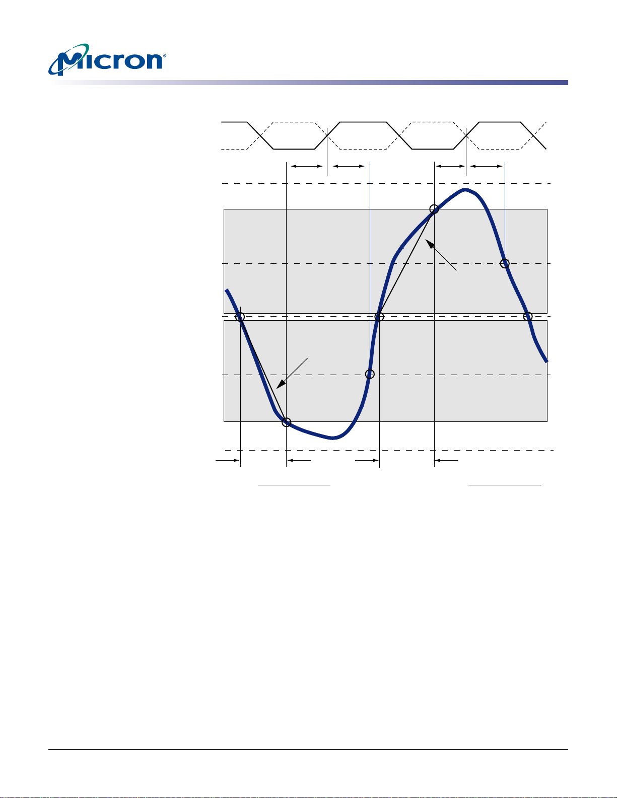
Figure 67: Nominal Slew Rate for tIS
CK
CK#
512Mb: x4, x8, x16 DDR2 SDRAM
Input Slew Rate Derating
VDDQ
V
IH(AC) MIN
VIH(DC) MIN
REF(DC)
V
V
IL(DC) MAX
IL(AC) MAX
V
VSS
Setup slew rate
falling signal
V
REF
to AC
region
t
IS
t
IH
t
IS
t
IH
Nominal
slew rate
Nominal
slew rate
V
REF
to AC
region
ΔTF
V
REF
(DC)
=
- VIL(AC) MAX
TF
Δ
ΔTR
Setup slew rate
rising signal
VIH(AC) MIN -
=
V
REF
(DC)
Δ
TR
PDF: 09005aef8117c18e, Source: 09005aef8211b2e6 Micron Technology, Inc., reserves the right to change products or specifications without notice.
512MbDDR2_2.fm - R ev. K 8/06 EN
90 ©2004 Micron Technology, Inc. All rights reserved.
Page 91
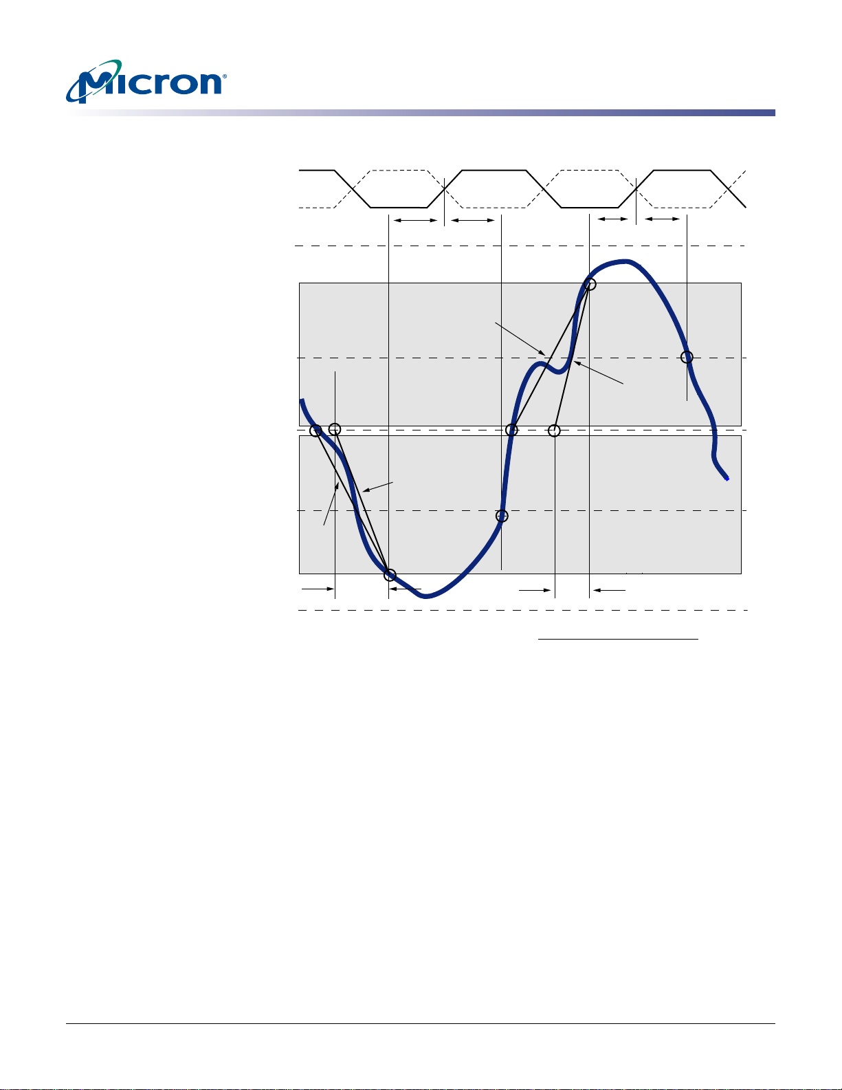
Figure 68: Tangent Line for tIS
CK
CK#
512Mb: x4, x8, x16 DDR2 SDRAM
Input Slew Rate Derating
IH(AC) MIN
V
IH(DC) MIN
V
REF(DC)
V
IL(DC) MAX
V
IL(AC) MAX
V
VDDQ
VSS
V
REF
to AC
region
Nominal
line
ΔTF
t
IS
Tangent
line
t
IH
Nominal
line
Setup slew rate
rising signal
t
IS
ΔTR
tangent line [VIH(AC) MIN - V
=
ΔTR
t
Tangent
line
IH
REF(DC
V
REF
to AC
region
)]
PDF: 09005aef8117c18e, Source: 09005aef8211b2e6 Micron Technology, Inc., reserves the right to change products or specifications without notice.
512MbDDR2_2.fm - R ev. K 8/06 EN
91 ©2004 Micron Technology, Inc. All rights reserved.
Page 92
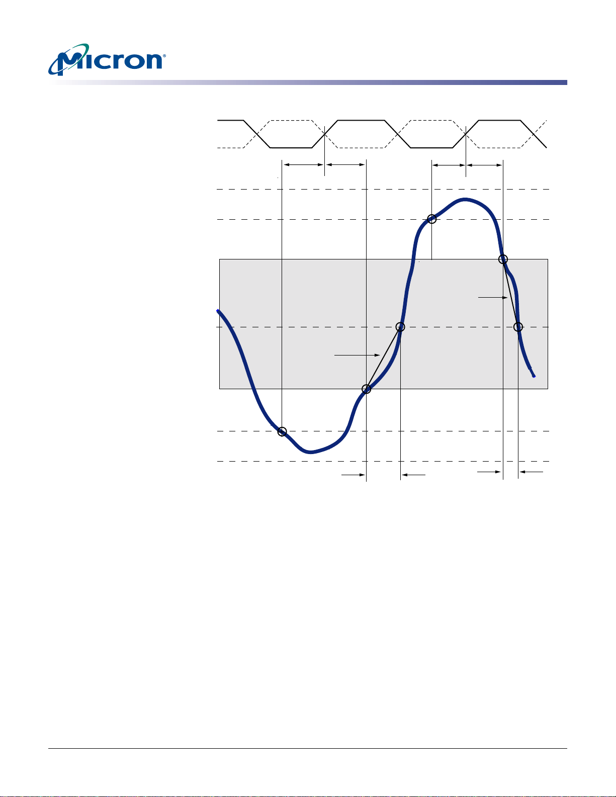
Figure 69: Nominal Slew Rate for tIH
CK
CK#
512Mb: x4, x8, x16 DDR2 SDRAM
Input Slew Rate Derating
VDDQ
V
IH(AC) MIN
IH(DC) MIN
V
REF(DC)
V
V
IL(DC) MAX
IL(AC) MAX
V
VSS
DC to V
region
REF
t
IS
t
IH
t
IS
t
IH
Nominal
slew rate
Nominal
slew rate
DC to V
REF
region
ΔTR
PDF: 09005aef8117c18e, Source: 09005aef8211b2e6 Micron Technology, Inc., reserves the right to change products or specifications without notice.
512MbDDR2_2.fm - R ev. K 8/06 EN
92 ©2004 Micron Technology, Inc. All rights reserved.
ΔTF
Page 93
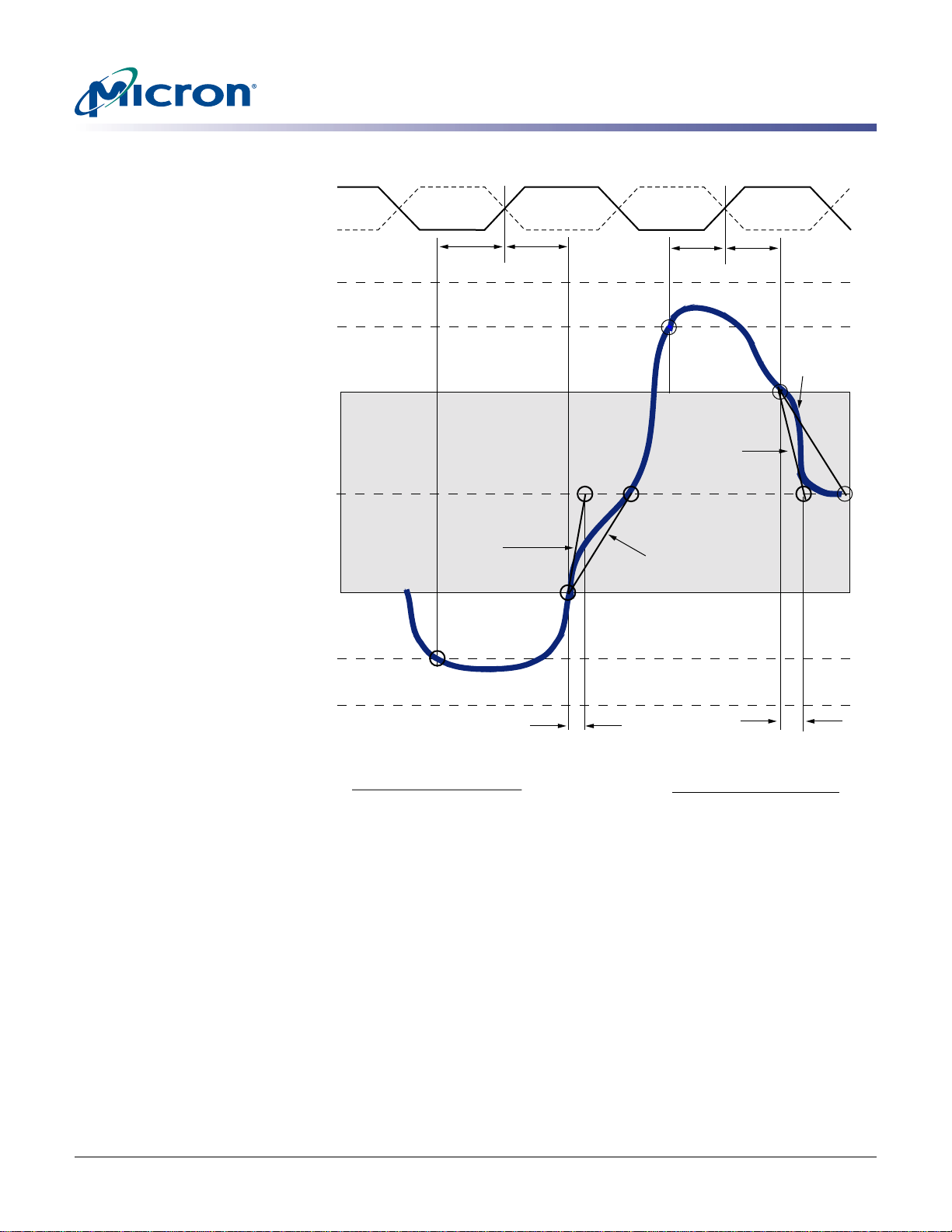
Figure 70: Tangent Line for tIH
CK
CK#
VDDQ
V
IH(AC) MIN
IH(DC) MIN
V
REF(DC)
V
V
IL(DC) MAX
DC to V
region
REF
512Mb: x4, x8, x16 DDR2 SDRAM
Input Slew Rate Derating
t
IS
t
IH
Tangent
line
Nominal line
t
IS
Tangent
line
DC to V
region
t
IH
Nominal
line
REF
IL(AC) MAX
V
VSS
Hold slew rate
rising signal
tangent line [VREF(DC) - VIL(DC) MAX]
=
ΔTR
ΔTR
Hold slew rate
falling signal
ΔTF
tangent line [VIH(DC) MIN - VREF(DC)]
=
ΔTF
PDF: 09005aef8117c18e, Source: 09005aef8211b2e6 Micron Technology, Inc., reserves the right to change products or specifications without notice.
512MbDDR2_2.fm - R ev. K 8/06 EN
93 ©2004 Micron Technology, Inc. All rights reserved.
Page 94
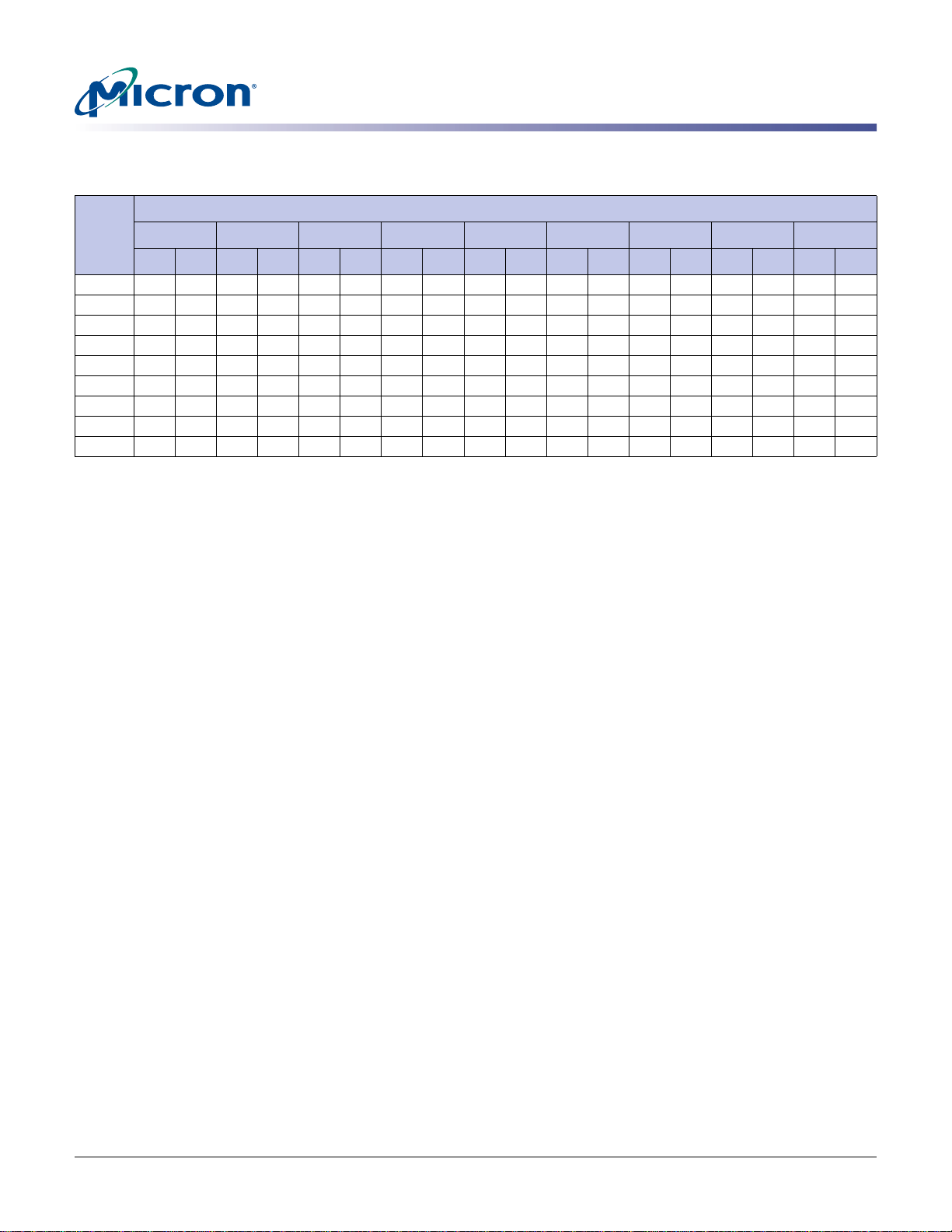
512Mb: x4, x8, x16 DDR2 SDRAM
Input Slew Rate Derating
Table 28: DDR2-400/533 tDS, tDH Derating Values with Differential Strobe
Notes: 1–7; all units in ps
DQ
Slew
Rate
(V/ns)
4.0 V/ns 3.0 V/ns 2.0 V/ns 1.8 V/ns 1.6 V/ns 1.4 V/ns 1.2 V/ns 1.0 V/ns 0.8 V/ns
ΔtDS ΔtDH ΔtDS ΔtDH ΔtDS ΔtDH ΔtDS ΔtDH ΔtDS ΔtDH ΔtDS ΔtDH ΔtDS ΔtDH ΔtDS ΔtDH ΔtDS ΔtDH
DQS, DQS# Differential Slew Rate
2.0125451254512545––––––––––––
1.5 8321832183219533 – – – – – – – – – –
1.000000012122424––––––––
0.9 – – –11 –14 –11 –14 1 –2 13 10 25 22 – – – – – –
0.8 – – – – –25 –31 –13 –19 –1 –7 11 5 23 17 – – – –
0.7–––––––31–42–19–30–7–185–6176––
0.6 – – – – – – – – –43 –59 –31 –47 –19 –35 –7 –23 5 –11
0.5 – – – – – – – – – – –74 –89 –62 –77 –50 –65 –38 –53
0.4 – – – – – – – – – – – – –127 –140 –115 –128 –103 –116
Notes: 1. For all input signals, the total tDS and tDH required is calculated by adding the data sheet
value to the derating value listed in Table 28.
t
DS nominal slew rate for a rising signal is defined as the slew rate between the last crossing
2.
of VREF(DC) and the first crossing of VIH(AC) MIN. tDS nominal slew rate for a falling signal is
defined as the slew rate between the last crossing of V
REF(DC) and the first crossing of
VIL(AC) MAX. If the actual signal is always earlier than the nominal slew rate line between
shaded “VREF(DC) to AC region ,” use no mi nal slew rate for derating value (see Figure 71). If
the actual signal is later than the nominal slew rate line anywhere between shaded
REF(DC) to AC region,” the slew rate of a tangent line to the actual signal from the AC
“V
level to DC level is used for derating value (see Figure 72).
t
3.
DH nominal slew rate for a rising signal is defined as the slew rate between the last crossing of VIL(DC) MAX and the first crossing of VREF(DC). tDH nominal slew rate for a falling signal is defined as th e slew ra te betw een the la st cross ing of V IH(DC) MIN and the first crossing
REF (DC). If the actual signal is always later than the nominal slew rate line between
of V
shaded “DC level to VREF(DC) region,” use nominal slew rate for derating value (see
Figure 73). If the actual signal is earlier than the nominal slew rate line anywhere between
shaded “DC to V
DC level to V
REF(DC) region,” the slew rate of a tangent line to the actual signal from the
REF(DC) level is used for derating value (see Figure 74).
4. Although the total setup time might be negative for slow slew rates (a valid input signal
will not have reached V
IH(AC)/VIL(AC) at the time of the rising clock transition), a valid input
signal is still required to complete the transition and reach VIH(AC)/VIL(AC).
5. For slew rates between the values listed in this table, the derating values may be obtained
by linear interpolation.
6. These values are typically not subject to production test. They are verified by design and
characterization.
7. Single-ended DQS requires special derating. The values in Table 30 are the DQS singleended slew rate derating with DQS referenced at V
t
DSb and tDHb. Table 31 provides the VREF-based fully derated values for the DQ (tDSa and
t
DHa) for DDR2-667. Table32 provides the VREF-based fully derated values for the DQ (tDSa
t
and
DHa) for DDR2-533. Table33 provides the VREF-based fully derated values for the DQ
t
DSa and tDHa) for DDR2-400.
(
REF and DQ referenced at the logic levels
PDF: 09005aef8117c18e, Source: 09005aef8211b2e6 Micron Technology, Inc., reserves the right to change products or specifications without notice.
512MbDDR2_2.fm - R ev. K 8/06 EN
94 ©2004 Micron Technology, Inc. All rights reserved.
Page 95
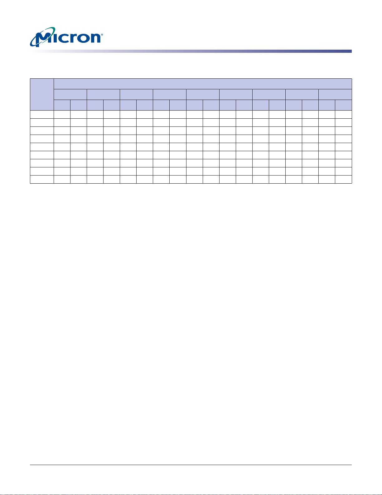
512Mb: x4, x8, x16 DDR2 SDRAM
Table 29: DDR2-667 tDS, tDH Derating Values with Differential Strobe
Notes: 1–7; all units in ps
Input Slew Rate Derating
DQ
Slew
Rate
(V/ns)
2.8 V/ns 2.4 V/ns 2.0 V/ns 1.8 V/ns 1.6 V/ns 1.4 V/ns 1.2 V/ns 1.0 V/ns 0.8 V/ns
ΔtDS ΔtDH ΔtDS ΔtDH ΔtDS ΔtDH ΔtDS ΔtDH ΔtDS ΔtDH ΔtDS ΔtDH ΔtDS ΔtDH ΔtDS ΔtDH ΔtDS ΔtDH
DQS, DQS# Differential Slew Rate
2.0 100 63 100 63 100 63 112 75 124 87 136 99 148 111 160 123 172 135
1.5 67 42 67 42 67 42 79 54 91 66 103 78 115 90 127 102 139 114
1.0 0 0 0 0 0 0 121224243636484860607272
0.9 –5–14–5–14–5–147 –219103122433455466758
0.8 –13 –31 –13 –31 –13 –31 –1 –19 11 –7 23 5 35 17 47 29 59 41
0.7 –22 –54 –22 –54 –22 –54 –10 –42 2 –30 14 –18 26 –6 38 6 50 18
0.6 –34 –83 –34 –83 –34 –83 –22 –71 –10 –59 2 –47 14 –35 26 –23 38 –11
0.5 –60 –125 –60 –125 –60 –125 –48 –113 –36 –101 –24 –89 –12 –77 0 –65 12 –53
0.4 –100 –188 –100 –188 –100 –188 –88 –176 –76 –164 –64 –152 –52 –140 –40 –128 –28 –116
Notes: 1. For all input signals the total tDS and tDH required is calculated by adding the data sheet
value to the derating value listed in Table 29.
t
DS nominal slew rate for a rising signal is defined as the slew rate between the last crossing
2.
of VREF(DC) and the first crossing of VIH(AC) MIN. tDS nominal slew rate for a falling signal is
defined as the slew rate between the last crossing of V
REF(DC) and the first crossing of
VIL(AC) MAX. If the actual signal is always earlier than the nominal slew rate line between
shaded “VREF(DC) to AC region ,” use no mi nal slew rate for derating value (see Figure 71). If
the actual signal is later than the nominal slew rate line anywhere between shaded
REF(DC) to AC region,” the slew rate of a tangent line to the actual signal from the AC
“V
level to DC level is used for derating value (see Figure 72).
t
3.
DH nominal slew rate for a rising signal is defined as the slew rate between the last
crossing of VIL(DC) MAX and the first crossing of VREF(DC). tDH nominal slew rate for a falling
signal is defined as the slew rate between the last crossing of VIH(DC) MIN and the first
crossing of V
REF (DC). If the actual signal is always later than the nominal slew rate line
between shaded “DC level to VREF(DC) region,” use nominal slew rate for derating value
(see Figure 73). If the actual signal is earlier than the nominal slew rate line anywhere
between shaded “DC to V
from the DC level to V
REF(DC) region,” the slew rate of a tangent line to the actual signal
REF(DC) level is used for derating value (see Figure 74).
4. Although the total setup time might be negative for slow slew rates (a valid input signal
will not have reached V
IH(AC)/VIL(AC) at the time of the rising clock transition), a valid input
signal is still required to complete the transition and reach VIH(AC)/VIL(AC).
5. For slew rates between the values listed in this table, the derating values may be obtained
by linear interpolation.
6. These values are typically not subject to production test. They are verified by design and
characterization.
7. Single-ended DQS requires special derating. The values in Table 30 are the DQS singleended slew rate derating with DQS referenced at V
t
DSb and tDHb. Table 31 provides the VREF-based fully derated values for the DQ (tDSa and
t
DHa) for DDR2-667. Table32 provides the VREF-based fully derated values for the DQ (tDSa
t
and
DHa) for DDR2-533. Table33 provides the VREF-based fully derated values for the DQ
t
DSa and tDHa) for DDR2-400.
(
REF and DQ referenced at the logic levels
PDF: 09005aef8117c18e, Source: 09005aef8211b2e6 Micron Technology, Inc., reserves the right to change products or specifications without notice.
512MbDDR2_2.fm - R ev. K 8/06 EN
95 ©2004 Micron Technology, Inc. All rights reserved.
Page 96
512Mb: x4, x8, x16 DDR2 SDRAM
Input Slew Rate Derating
Table 30: Single-Ended DQS Slew Rate Derating Values Using
t
DS
b
and
t
DH
b
Reference points indicated in bold
DQS Single-Ended Slew Rate Derated (at VREF)
DQ
(V/ns)
2.0 V/ns 1.8 V/ns 1.6 V/ns 1.4 V/ns 1.2 V/ns 1.0 V/ns 0.8 V/ns 0.6 V/ns 0.4V/ns
t
DStDHtDStDHtDStDHtDStDHtDStDHtDStDHtDStDHtDStDHtDStDH
2 130 53 130 53 130 53 130 53 130 53 145 48 155 45 165 41 175 38
1.59732973297329732973211227122241322014217
1 30–1030–1030–1030–1030–1045 –15 55 –18 65 –22 75 –25
0.9 25 –24 25 –24 25 –24 25 –24 25 –24 40 –29 50 –32 60 –36 70 –39
0.8 17 –41 17 –41 17 –41 17 –41 17 –41 32 –46 42 –49 52 –53 61 –56
0.7 5 –64 5 –64 5 –64 5 –64 5 –64 20 –69 30 –72 40 –75 50 –79
0.6 –7 –93 –7 –93 –7 –93 –7 –93 –7 –93 8 –98 18 –102 28 –105 38 –108
0.5 –28 –135 –28 –135 –28 –135 –28 –135 –28 –135 –13 –140 –3 –143 7 –147 17 –150
0.4 –78 –198 –78 –198 –78 –198 –78 –198 –78 –198 –63 –203 –53 –206 –43 –210 –33 –213
Notes: 1. Derating values, to be used with base tDSb- and tDHb-specified values.
Table 31: Single-Ended DQS Slew Rate Fully Derated (DQS, DQ at VREF) at DDR2-667
Reference points indicated in bold
DQS Single-Ended Slew Rate Derated (at VREF)
DQ
(V/ns)
1.5 330 290 330 290 330 290 330 290 330 290 345 285 355 282 365 279 375 275
0.9 347 290 347 290 347 290 347 290 347 290 362 285 372 282 382 278 392 275
0.8 367 290 367 290 367 290 367 290 367 290 382 285 392 282 402 278 412 275
0.7 391 290 391 290 391 290 391 290 391 290 406 285 416 281 426 278 436 275
0.6 426 290 426 290 426 290 426 290 426 290 441 285 451 282 461 278 471 275
0.5 472 290 472 290 472 290 472 290 472 290 487 285 497 282 507 278 517 275
0.4 522 289 522 289 522 289 522 289 522 289 537 284 547 281 557 278 567 274
2.0 V/ns 1.8 V/ns 1.6 V/ns 1.4 V/ns 1.2 V/ns 1.0 V/ns 0.8 V/ns 0.6 V/ns 0.4V/ns
t
DStDHtDStDHtDStDHtDStDHtDStDHtDStDHtDStDHtDStDHtDStDH
2 330 291 330 291 330 291 330 291 330 291 345 286 355 282 365 29 375 276
1 330 290 330 290 330 290 330 290 330 290 345 285 355 282 365 278 375 275
PDF: 09005aef8117c18e, Source: 09005aef8211b2e6 Micron Technology, Inc., reserves the right to change products or specifications without notice.
512MbDDR2_2.fm - R ev. K 8/06 EN
96 ©2004 Micron Technology, Inc. All rights reserved.
Page 97
512Mb: x4, x8, x16 DDR2 SDRAM
Input Slew Rate Derating
Table 32: Single-Ended DQS Slew Rate Fully Derated (DQS, DQ at VREF) at DDR2-533
Reference points indicated in bold
DQS Single-Ended Slew Rate Derated (at VREF)
DQ
(V/ns)
1.5 364 340 364 340 364 340 364 340 364 340 379 335 389 332 399 329 409 325
0.9 402 340 402 340 402 340 402 340 402 340 417 335 427 332 437 328 447 325
0.8 429 340 429 340 429 340 429 340 429 340 444 335 454 332 464 328 474 325
0.7 463 340 463 340 463 340 463 340 463 340 478 335 488 331 498 328 508 325
0.6 510 340 510 340 510 340 510 340 510 340 525 335 535 332 545 328 555 325
0.5 572 340 572 340 572 340 572 340 572 340 587 335 597 332 607 328 617 325
0.4 647 339 647 339 647 339 647 339 647 339 662 334 672 331 682 328 692 324
Table 33: Single-Ended DQS Slew Rate Fully Derated (DQS, DQ at VREF) at DDR2-400
2.0 V/ns 1.8 V/ns 1.6 V/ns 1.4 V/ns 1.2 V/ns 1.0 V/ns 0.8 V/ns 0.6 V/ns 0.4V/ns
t
DStDHtDStDHtDStDHtDStDHtDStDHtDStDHtDStDHtDStDHtDStDH
2 355 341 355 341 355 341 355 341 355 341 370 336 380 332 390 329 400 326
1 380 340 380 340 380 340 380 340 380 340 395 335 405 332 415 328 425 325
Reference points indicated in bold
DQS Single-Ended Slew Rate Derated (at VREF)
2.0 V/ns 1.8 V/ns 1.6 V/ns 1.4 V/ns 1.2 V/ns 1.0 V/ns 0.8 V/ns 0.6 V/ns 0.4V/ns
DQ
(V/ns)
t
DStDHtDStDHtDStDHtDStDHtDStDHtDStDHtDStDHtDStDHtDStDH
2 405 391 405 391 405 391 405 391 405 391 420 386 430 382 440 379 450 376
1.5 414 390 414 390 414 390 414 390 414 390 429 385 439 382 449 379 459 375
1 430 390 430 390 430 390 430 390 430 390 445 385 455 382 465 378 475 375
0.9 452 390 452 390 452 390 452 390 452 390 467 385 477 382 487 378 497 375
0.8 479 390 479 390 479 390 479 390 479 390 494 385 504 382 514 378 524 375
0.7 513 390 513 390 513 390 513 390 513 390 528 385 538 381 548 378 558 375
0.6 560 390 560 390 560 390 560 390 560 390 575 385 585 382 595 378 605 375
0.5 622 390 622 390 622 390 622 390 622 390 637 385 647 382 657 378 667 375
0.4 697 389 697 389 697 389 697 389 697 389 712 384 722 381 732 378 742 374
PDF: 09005aef8117c18e, Source: 09005aef8211b2e6 Micron Technology, Inc., reserves the right to change products or specifications without notice.
512MbDDR2_2.fm - R ev. K 8/06 EN
97 ©2004 Micron Technology, Inc. All rights reserved.
Page 98
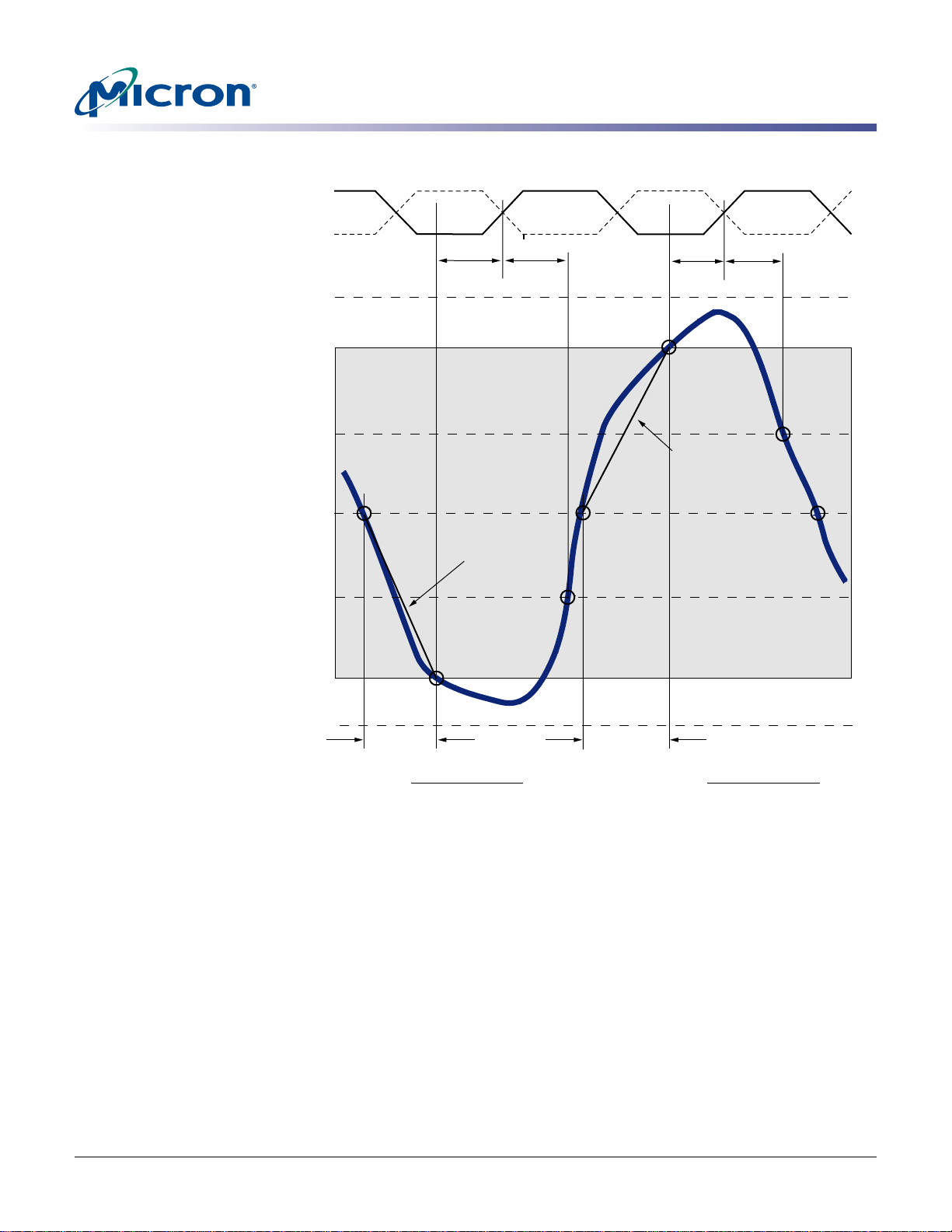
Figure 71: Nominal Slew Rate for tDS
1
DQS
1
DQS#
512Mb: x4, x8, x16 DDR2 SDRAM
Input Slew Rate Derating
VDDQ
V
IH(AC) MIN
IH(DC) MIN
V
REF(DC)
V
IL(DC) MAX
V
IL(AC) MAX
V
V
REF
region
to AC
t
DS
Nominal
slew rate
t
DH
t
DS
t
DH
Nominal
slew rate
REF
to AC
V
region
VSS
Δ
Setup slew rate
falling signal
=
TF
VREF(DC)
- VIL(AC) MAX
ΔTF
Δ
TR
Setup slew rate
rising signal
VIH(AC) MIN -
=
VREF(DC)
ΔTR
Notes: 1. DQS, DQS# signals must be monotonic between VIL(DC) MAX and VIH(DC) MIN.
PDF: 09005aef8117c18e, Source: 09005aef8211b2e6 Micron Technology, Inc., reserves the right to change products or specifications without notice.
512MbDDR2_2.fm - R ev. K 8/06 EN
98 ©2004 Micron Technology, Inc. All rights reserved.
Page 99
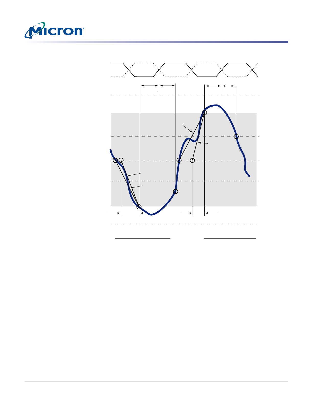
Figure 72: Tangent Line for tDS
1
DQS
1
DQS#
512Mb: x4, x8, x16 DDR2 SDRAM
Input Slew Rate Derating
VDDQ
V
IH(AC) MIN
IH(DC) MIN
V
REF(DC)
V
V
IL(DC) MAX
IL(AC) MAX
V
VSS
Setup Slew Rate
Falling Signal
V
REF
to AC
region
tangent line [V
=
Δ
TF
t
DS
Tangent line
Nominal line
REF(DC
) - VIL(AC) MAX]
ΔTF
t
DH
Nominal
line
Δ
TR
Setup Slew Rate
Rising Signal
t
DS
Tangent line
tangent line [V
=
t
DH
IH(AC
ΔTR
V
REF
to AC
region
) MIN - V
REF(DC
)]
Notes: 1. DQS, DQS# signals must be monotonic between VIL(DC) MAX and VIH(DC) MIN.
PDF: 09005aef8117c18e, Source: 09005aef8211b2e6 Micron Technology, Inc., reserves the right to change products or specifications without notice.
512MbDDR2_2.fm - R ev. K 8/06 EN
99 ©2004 Micron Technology, Inc. All rights reserved.
Page 100
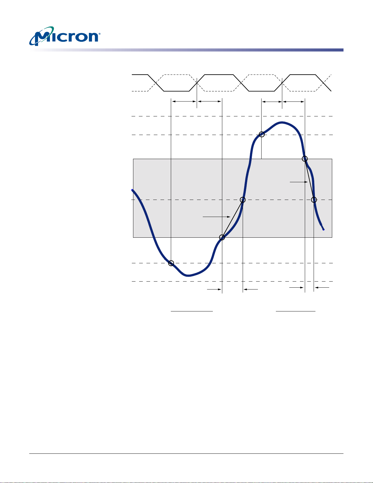
Figure 73: Nominal Slew Rate for tDH
1
DQS
1
DQS#
512Mb: x4, x8, x16 DDR2 SDRAM
Input Slew Rate Derating
VDDQ
V
IH(AC) MIN
IH(DC) MIN
V
REF(DC)
V
V
IL(DC) MAX
IL(AC) MAX
V
VSS
DC to V
region
REF
t
IS
t
IH
t
IS
t
IH
Nominal
slew rate
Nominal
slew rate
DC to V
REF
region
ΔTF
VREF(DC)
ΔTF
Hold slew rate
rising signal
VREF(DC) -
=
VIL(DC) MAX
ΔTR
ΔTR
Hold slew rate
falling signal
VIH(DC) MIN -
=
Notes: 1. DQS, DQS# signals must be monotonic between VIL(DC) MAX and VIH(DC) MIN.
PDF: 09005aef8117c18e, Source: 09005aef8211b2e6 Micron Technology, Inc., reserves the right to change products or specifications without notice.
512MbDDR2_2.fm - R ev. K 8/06 EN
100 ©2004 Micron Technology, Inc. All rights reserved.
 Loading...