

Page 1

INTEGRATED CIRCUITS
P32P4910B
PRML Read Channel with PR4,
8/9 ENDEC, 4-Burst Servo
Product specification 1997 July 15
Page 2

Philips Semiconductors Product specification
PRML Read Channel with PR4,
8/9 ENDEC, 4-Burst Servo
GENERAL DESCRIPTION
The Philips Semiconductors P32P4910B is a high performance
BiCMOS read channel IC that provides all of the functions needed to
implement an entire Partial Response Class 4 (PR4) read channel
for zoned recording hard disk drive systems with data rates from
42 to 125 Mbit/s or 33 to 100 Mbit/s. Functional blocks include
AGC, programmable filter, adaptive transversal filter, Viterbi qualifier ,
8,9 GCR ENDEC, data synchronizer, time base generator, and
4-burst servo.
Programmable functions such as data rate, filter cutoff, filter boost,
etc., are controlled by writing to the serial port registers so no
external component changes are required to change zones.
The part requires a single +5V power supply. The Philips
Semiconductors P32P4910B utilizes an advanced BiCMOS process
technology along with advanced circuit design techniques which
result in high performance devices with low power consumption.
FEA TURES
General:
•Register programmable data rates from 42 to 125 Mbit/s or
33 to 100 Mbit/s
•Sampled data read channel with Viterbi qualification
•Programmable filter for PR4 equalization
•Five tap transversal filter with adaptive PR4 equalization
•8/9 GCR ENDEC
•Data Scrambler/Descrambler
•Presettable precoder state
•Programmable write precompensation
•Low operating power (0.85 W typical at 5V)
•Register programmable power management
(<5 mW power down mode)
•4-bit nibble and byte-wide bi-directional NRZ data interfaces
•I/O Mapping and In circuit test
•8-bit Direct Write mode automatically configured for
RCLK = VCO/8
•Thermal asperity detection and suppression
•Bi-directional serial interface port for access to internal program
storage registers (read and write capability)
•Single power supply (5V ± 10%)
•Small footprint, 100-lead LQFP package
P32P4910B
Automatic Gain Control:
•Dual mode AGC, analog during acquisition, sampled during data
reads
•Separate AGC level storage pins for data and servo
•Dual rate attack and decay charge pump for rapid AGC recovery
(analog)
•Programmable, symmetric, charge pump currents for data reads
(sampled)
•Charge pump currents track programmable data rate during data
reads (sampled)
•Low drift AGC hold circuitry
•Low-Z circuitry at AGC input provides for rapid external coupling
capacitor recovery
•AGC Amplifier squelch during Low-Z
•Wide bandwidth, precision full-wave rectifier
•Programmable AGC controls
– Separate external input pins for AGC hold, fast recovery, and
Low-Z control
or
– Internal Low-Z and fast decay timing for rapid transient
recovery and AGC acquisition. Timing set with external
resistors (2). Ultra fast decay current set with external resistor.
AGC input impedance vs LOWZ = 5:1.
•2-bit DAC to control AGC voltage in servo mode between 1.1
and 1.4 V
Filter/Equalizer:
•Programmable, 7-pole, continuous time filter provides:
– Channel filter and pulse slimming equalization for equalization
to PR4
– Programmable cutoff frequency from 4 to 34 MHz
– Programmable boost /equalization of 0 to 13 dB
– Programmable “zeros” equalization provides time asymmetry
compensation
– ±0.5 ns group delay variation from 0.3ƒc to ƒc, with
ƒc = 34 MHz
– Minimizes size and power
– Low-Z switch at filter output for fast offset recovery
– No external coupling capacitors required
– DC offset compensation provided at filter output
– Five tap transversal filter for fine equalization to PR4
– Self adapting inner taps (symmetric)
– Programmable outer taps (symmetric, 4-bits)
– Equalization hold input
– “Zeros” channel quality output
– Amplitude asymmetry factor output
1997 JuL 15 853-1952 18177
2
Page 3

Philips Semiconductors Product specification
PRML Read Channel with PR4,
8/9 ENDEC, 4-Burst Servo
Pulse Qualification:
•Sampled Viterbi qualification of signal equalized to PR4
•Register programmable window or hysteresis pulse qualifier for
servo reads
•Selectable RDS pulse width and polarity for servo gray code reads
Time Base Generator:
•Less than 1% frequency resolution
•Up to 141 MHz frequency output
•Independent M and N divide-by registers
•No active external components required
Data Separator:
•Fully integrated data separator includes data synchronizer and
8,9 GCR ENDEC
•Register programmable to 125 Mbit/s operation
•Fast Acquisition, sampled data phase lock loop
•Decision directed clock recovery from data samples
•Adaptive clock recovery thresholds
•Programmable damping ratio for data synchronizer PLL is
constant for all data rates
•Data scrambler/descrambler to reduce fixed pattern effects
•4-bit nibble and byte-wide NRZ data interfaces
•Time base tracking, programmable write precompensation
•Differential PECL write data output
•Integrated sync byte detection, single byte or dual (“or” type)
P32P4910B
•Semi-auto training and sync byte generation available for single
sync byte operation
•Surface defect scan mode
Servo:
•4-burst servo capture with A, B, C, D outputs
•Internal hold capacitors
•“Soft Landing” charge pump architecture
•Separate, automatically selected, registers for servo ƒc, boost,
and threshold
•Programmable charge pump current
•Wide bandwidth, precision full-wave rectifier
•Programmable selection of normal or differentiated filter output to
servo capture block
•Programmable AGC gain in servo mode (2-bits)
•Full wave rectifier observation point
Thermal Asperity:
•Internal TA detector that monitors DP/DN output of continuous
time filter
•Hi-Y input modulation to rapidly attenuate offset due to TA
•AGC and PLL hold that may be triggered by TA event
•EFLAG output is dynamically generated to flag TA corrupted NRZ
data
•TAD input pin allows use of an external TA event detector
1997 JuL 15
3
Page 4

Philips Semiconductors Product specification
PRML Read Channel with PR4,
8/9 ENDEC, 4-Burst Servo
BLOCK DIAGRAM
WCLK
NRZ0–7
SYNC
BYTE
DETECTOR
PARALLEL
INTERFACE
DESCRAMBLER
9,8
DECODER
DSCLK
TO
SERIAL
PARALLEL
DUAL BIT
SCRAMBLER
9,8
BOUNDRY
CODE WORD
DB0–DB1
INTERFACE
ENCODER
CWBD
DETECTOR
RCLK
DWI
DWI
PRECODER
TO
PARALLEL
MUX
SERIAL
WD
WD
MUX
WRITE
FLIP-FLOP
MUX
WRITE
PRECOMP
MUX
GEN
PATTERN
VCO SYNC
DWR
TBGOUT
NCLK
RCLK
RCLK
CWBD
DSCLK
CHARGE
DATA SYNCHRONIZER
PHASE
DECISION
DIRECTED
DETECTOR
RCLK
GEN
CLOCK
VCO
PUMP
TBGOUT
FREQ
PHASE/
DAMPING
DETECTOR
ATO
DAC
CONTROL
TEST
ATRN
MUX
TBGOUT
POWER
TIME BASE GENERATOR
DOWN
CONTROL
P32P4910B
AGND3
AGND2
AGND1
DGND2
DGND1
PDWN
VPA3
VPA2
VPA1
VPD2
VPD1
FLTR2–
FLTR2+
VCO
FLTR1–
FLTR1+
PUMP
RR
CHARGE
FREQ
PHASE/
DETECTOR
1/(N+1)
1/(M+1)
FREF
SM00171
VRDT
TPB–
TPB+
TPA–
TPA+
PPOL
Σ
1/12
REF
3.2V
LOGIC
CONTROL
RG
WG
D
Σ
C
B
A
Philips Semiconductors P32P4910B
MAXREF
STROBE
RESET
SYNC
FIELD
TAD
VREF
COUNTER
REGISTERS
SDATA
Σ
Σ
LOGIC
DECODE
SG
QUAL
FROM LEVEL
DSCLK
FULLWAVE
RECTIFIER
SFWR
AGC
CONV
PUMP
CHARGE
AGC
CONTROL
AGC
PUMP
CHARGE
SAMPLED
VRC
LOWZ
LOGIC
FASTREC
x3
x3
x3
x3
+
–
VREF
&
PORT
SERIAL
CONTROL
SCLK
SDEN
MUX
MUX
TEST POINY
VITERBI
DETECTOR
RDS
CP
CN
DP
DN
ON+
ON–
OD+
OD–
VRX
To SFC
QUAL
PULSE
LEVEL TYPE
FILTER
LOW PASS
7TH ORDER
PROGRAMMABLE
AGC
AMP
VIA–
VIA+
BYPS
TA
BYP
3–TAP
ADAPTIVE
&
SAMPLE
EQUALIZER
HOLD
PLL
AGC
HOLD
1997 JuL 15
4
Page 5

Philips Semiconductors Product specification
PRML Read Channel with PR4,
8/9 ENDEC, 4-Burst Servo
P32P4910BP Pinout – 100 LQFP
VIA+
NC
NC
NC
BYPD
BYPS
HOLD
LOWZ
FASTREC
VRDT
SCLK
SDATA
SDEN
VPF
FREF
VNF
VPT
FLTR1+
FLTR1–
VNT
DWI
DWI
WD
WD
NC
NC
NC
NC
1
2
3
4
5
6
7
8
9
10
11
12
13
14
15
16
17
18
19
20
21
22
23
24
25
26 27 28 29 30 31 32 33
VIA–
VRX
VPA
AGCDEL
WRDEL
AGCRST
TPC–
919293949596979899100
TPC+
TPD–
TPD+
TPE
403937 38363534
VNA
PPOL/EFLAG
SG
BURST A
RDS/RDS/TAD
81828384858687888990 80 79 7678 77
44434241
BURST C
BURST B
BURST D
NC
48474645 5049
NC
P32P4910B
NC
75
TAD
74
EFLAG
73
VRC
72
RR
71
MAXREF
RESET
70
69
STROBE
68
VPS
67
VNS
66
TPA+
65
TPA–
64
TPB+
63
TPB–
62
VPS
61
ATO
60
EQHOLD
59
VNS
58
VPP
57
FLTR2+
56
FLTR2–
55
VNP
54
VNC
53
NC
52
NC
51
NC
1997 JuL 15
NC
RG
WG/WG
SBD
PERRNCNRZP
NRZ0
NRZ1
NRZ2
NRZ3
VND
VPD
5
NRZ4
NRZ5
NRZ6
NRZ7
WCLK
RCLK
DWR
PDWN
VPC
NC
NC
NC
SM00172
Page 6

Philips Semiconductors Product specification
PRML Read Channel with PR4,
8/9 ENDEC, 4-Burst Servo
FUNCTIONAL DESCRIPTION
The Philips Semiconductors P32P4910B implements a complete
high performance PR4 read channel, including an AGC,
programmable filter/equalizer, adaptive transversal filter, Viterbi
pulse qualifier, time base generator, data separator with 8,9 ENDEC
and scrambler/descrambler , and 4-burst capture servo, that
supports data rates from 42 to 125 Mbit/s. Data rates from 33 to
100 Mbit/s are supported by changing a single resistor.
A serial port is provided to write control data to the internal program
storage registers.
AGC Circuit
The automatic gain control (AGC) circuit is used to maintain a
constant signal amplitude at the input of the pulse detector and
sampled data processor while the input to the amplifier varies. The
circuit consists of an AGC loop that includes an AGC amplifier,
charge pump, programmable continuous time filter, and a precision,
wide band, full wave rectifier. Depending on whether the read is of
servo or data type, the specific blocks utilized in the loop are slightly
different. Both loop paths are fully differential to minimize
susceptibility to noise. AGC control can be programmably selected
between direct and timed modes.
AGC Operation in Servo Read Mode
During servo reads the loop consists of the AGC amplifier with a
continuous dual rate charge pump, the programmable continuous
time filter, and the full wave rectifier. The gain of the AGC amplifier
is controlled by the voltage stored on the BYPS hold capacitor
(C
The dual rate charge pump drives C
BYPS).
drive the differential voltage at DP/DN (internal nodes) to the value
programmed by the 2 SAGCLVL bits in the LDS register. These
2 bits allow adjustment of the filter’s normal output voltage from
1.10 to 1.40 Vppd. Attack currents lower the voltage at the BYPS
pin which reduces the amplifier gain. Decay currents raise the
voltage at the BYPS pin which increases the amplifier gain. The
sensitivity of the amplifier gain to changes in the BYPS voltage is
approximately 38 dB/V. When the voltage at BYPS is equal to VRC,
the gain from the AGC input to DP/DN will be about 24.9 dB. The
charge pump is continuously driven by the instantaneous voltage at
DP/DN. When the signal at DP/DN is greater than 100% of the
programmed AGC level, the normal attack current (I
used to reduce the amplifier gain. If the signal is greater than 125%
of the programmed level, the fast attack current (I
2.86 mA is used to reduce the gain very quickly. This dual rate
approach allows the AGC gain to be quickly decreased when it is
too high and minimizes distortion when the proper AGC level has
been acquired. The 100% and 125% levels are relative to the
selected AGC level in servo mode.
A constant normal decay current (I
amplifier gain when the signal at DP/DN is less than 100% of the
programmed AGC level. The large ratio (340 µA:20 µA) of the
normal attack and normal decay currents enables the AGC loop to
respond to the peak amplitudes of the incoming read signal rather
than the average value. As a result the AGC loop will not be able to
quickly increase its gain if required to do so. A fast recovery mode
is provided to allow the gain to be rapidly increased to reduce
recovery time between mode switches. In the fast recovery mode,
the decay current is increased by a factor of 8 to 160 µA (I
the attack current is increased by a factor of 4.18 to 1.42 mA (I
This has the effect of speeding up the AGC loop between 4 and 8
times.
) of 20 µA acts to increase the
D
with currents that
BYPS
CH
) of
CHF
) of 340 µA is
) and
DFR
CHFR
P32P4910B
It is recommended that the fast recovery mode be asserted when
the AGC fields from a sector are being read. Typically, this will be
just after each transition of SG (Servo Gate), after powerup, and
after WG/WG
FASTREC is asserted for 0.5
can increase at most by 0.5 µs * 160 µA/500 pF = 160 mV, which
will allow the gain to increase by 6 dB in that time. If FASTREC is
asserted for 0.5 µs in non-servo mode and C
the voltage at BYPD can increase at most by 0.5 µs * 160 µA/1000
pF = 80 mV, which will allow the gain to increase by 3 dB in that
time. It is recommended that LOWZ be asserted for 0.5 µs just prior
to any assertion of FASTREC in order to null any internal DC offsets.
However, it is possible to assert both LOWZ and FASTREC
simultaneously to reduce sector overhead. This method should be
evaluated under the actual system operating conditions.
The programmable AGC level in servo mode is provided to allow the
servo demodulator dynamic range to be adjusted over a narrow
range.
AGC Operation in Data Read Mode
For data reads, the loop described above is used until the data
synchronizer is locked to the incoming VCO preamble, except that
the BYPD hold capacitor (C
(C
BYPS
current is 2.86 mA, and the fast attack current is 2.86 mA. The fast
recovery mode decay current is 160 µA and the fast recovery mode
attack current is 1.42 mA. The above mentioned attack and decay
currents are not scaled with the data rate setting. After the data
synchronizer PLL is locked (SFC), the AGC loop is switched to
include the AGC amplifier with a sampled charge pump, the
programmable continuous time filter, full wave rectifier, and the
sampling 5-tap equalizer to more accurately control the signal
amplitude into the Viterbi qualifier. In this sampled AGC mode, a
symmetrical attack and decay charge pump is used. The “1” sample
amplitudes are sampled, held and compared to the ideal “1” value of
500 mV to generate the error current. The maximum charge pump
current value can be programmed from the Sample Loop Control
Register to 0, 34, 68, or 102 µA for maximum data rate and will
scale downward with reduced Data Rate Register values.
AGC Control Modes
The AGC control mode is determined by the state of bit 6 (AGCSEL)
of the Control Operating Register #1.
external AGC control method is selected. For example, AGC uses
external signals provided to the FASTREC, LOWZ, and HOLD
pins. If bit 6 is a 1, the timed AGC control method is selected for
generating the internal hold, fast recovery, squelch, and Low-Z
signals.
Direct AGC Control Mode
For maximum application flexibility, all AGC mode control inputs are
to be externally provided. When the LOWZ input is High, Low-Z
mode is activated. In the Low-Z mode, the AGC amplifier input
resistance is reduced to allow quick recovery of the AGC amplifier
input AC coupling capacitors. The ratio of Low-Z to non Low-Z
resistance can be selected as either 15:1 or 5:1 by programming the
LZTC bit in the Data Boost Register. During Low-Z mode, the time
constant of the internal AC coupling networks at the filter outputs are
also reduced by the ratio determined by the LZTC bit. This time
).
constant is 300 ns in Low-Z and either 5 µs or 1.5 µs when not in
Low-Z mode, depending on the state of the LZTC bit. Low-Z also
forces the AGC amplifier gain to be reduced to near 0 V/V . This
is de-asserted. For example, if C
µs in servo mode, the voltage at BYPS
) is used instead of BYPS and
). The normal decay current is 20 µA, the normal attack
BYPD
If this bit is 0, then the direct,
is 500 pF and
BYPS
is 1000 pF, then
BYPD
input
1997 JuL 15
6
Page 7

Philips Semiconductors Product specification
PRML Read Channel with PR4,
8/9 ENDEC, 4-Burst Servo
mode should be activated during and for a short time after a write
operation. It should also be activated for a short time after each
transition of the SG input and on initial power up.
When the HOLD
de-activates the AGC loop. The AGC amplifier gain will be held
constant at a level set by the voltage at the BYPD or BYPS pins.
The value of the capacitor placed at these pins should be selected
to give adequate droop performance when in hold mode as well as
to insure stability of the AGC loop when it is active.
The signal provided to the FASTREC input pin determines if the
AGC is in fast recovery mode. During the fast recovery
(FASTREC=1), the attack and decay currents are increased to allow
faster recovery to the proper AGC level. If faster recovery than is
provided by FASTREC alone is desired, an ultra fast recovery can
be effected by connecting a resistor between the AGCRST pin and
the positive supply VPA. If this resistor is present, whenever
FASTREC is entered, the voltage on the BYPD or BYPS capacitor
will be pulled up. This causes an extremely rapid increase in the
AGC amplifier gain. The ultra fast current will be disabled the first
time that the signal at DP/DN reaches the 125% point. The
FASTREC attack and decay currents are used as long as the
FASTREC pin is held High.
input is Low, the charge pumps are disabled. This
P32P4910B
Timed AGC Control mode
This timed AGC control mode differs from the direct control mode in
that the external control inputs LOWZ, FASTREC, and HOLD
typically not used, and therefore, must be deasserted. The
equivalent signals are generated internal to the P32P4910B. These
internal signals are generated by one-shots that are triggered by
various conditions of the WG/WG
, SG, and PDWN inputs. The
one-shot timings for the Low-Z and fastrec signals are set by the
resistors connected to the WRDEL and AGCDEL input pins,
respectively and analog ground.
The time Low-Z period (µs) = 0.1 * [0.5 + R
recovery period (µs) = 0.1 * [0.5 + R
AGCDEL
(kΩ)] and the fast
WRDEL
(kΩ)]. The current for
the ultra fast decay mode is set by the resistor connected between
the AGCRST input pin and VPA. In the timed mode, the AGC shall
use the C
BYPD
and C
for non-servo and servo modes
BYPS
respectively. The nominal and fast attack and decay currents are
the same in both of the P32P4910B’s AGC control modes. In
internally timed mode, the LOWZ, FASTREC, and HOLD
are logically OR’ed with their respective internal control signals but
do not affect the internal sequencing of the one-shot generated AGC
control signals.
, are
input pins
AGC
INPUT
PDWN
AGC LOWZ
FAST FILTER
OFFSET RECOVERY
AGC HOLD
AGC SQUELCH
AGC FAST RECOVERY
(ATTACK & DECAY)
AGC ULTRA
FAST RECOVERY
(DECAY)
OUTPUT
AGC
POWERED UP
t
LZ
t
LZ
t
LZ
t
LZ
t
FD
Ultra fast decay current is disabled when signal is greater
than 125% of nominal.
+
–
ULTRA
FAST
DECAY
FAST
ATTACK
NORMAL
ATTACK
125%
100%
SM00173
Figure 1. Power-On Mode Gain Recovery
1997 JuL 15
7
Page 8

Philips Semiconductors Product specification
PRML Read Channel with PR4,
8/9 ENDEC, 4-Burst Servo
AGC
INPUT
SG
AGC LOWZ
FAST FILTER
OFFSET RECOVERY
AGC HOLD
SQUELCH
AGC FAST RECOVERY
(ATTACK & DECAY)
AGC ULTRA
FAST RECOVERY
(DECAY)
+
AGC OUTPUT
–
ULTRA
FAST
DECAY
t
LZ
Figure 2. Servo Mode Gain Recovery
t
FD
FAST
ATTACK
t
LZ
t
LZ
t
FD
Ultra fast decay current is disabled when
signal is greater than 125% of nominal.
125%
100%
P32P4910B
SM00165
AGC
INPUT
WG
AGC LOWZ
FAST FILTER
OFFSET RECOVERY
AGC HOLD
AGC SQUELCH
AGC FAST RECOVERY
(ATTACK & DECAY)
AGC ULTRA
FAST RECOVERY
(DECAY)
+
AGC
OUTPUT
–
Ultra fast decay current is disabled when
signal is greater than 125% of nominal.
ULTRA
FAST
DECAY
t
LZ
t
LZ
t
FD
125%
100%
NORMAL
ATTACK
FAST
ATTACK
SM00166
1997 JuL 15
Figure 3. Write Mode Gain Recovery
8
Page 9

Philips Semiconductors Product specification
PRML Read Channel with PR4,
8/9 ENDEC, 4-Burst Servo
Pulse Qualification Circuit
This device utilizes three different types of pulse qualification, one
exclusively for servo reads, one primarily for servo reads, and the
other for data reads.
Servo Read Mode
For servo gray code reads, either a dual level (window type) qualifier
or a hysteresis type level qualifier may be selected. If the PDM bit in
the Filter Cutoff Servo Register is set to 0, then the window qualifier
is selected, and if the PDM bit equals 1, the hysteresis qualifier is
selected. The polarity of the RDS/RDS
(Servo Mode Select) in the Data Rate Register. If SMS is set to 0,
then RDS is active-Low and if SMS bit equals 1, then RDS is
active-High.
Dual Level (Window) Qualifier
During servo reads (SG High) a dual level type of pulse qualifier is
used. The level qualification thresholds are set by a 6-bit DAC
which is controlled by the Servo Level Threshold Register (LDS).
The register value is relative to the peak voltage at the output of the
continuous time filter derived off of the same reference voltage
internal to the chip. The positive and negative thresholds are equal
in magnitude. The state of the adaptive threshold level enable
(ALE) bit in the WP/LT Register does not affect this DAC’s
reference. The RDS/RDS
qualifier indicate a qualified servo pulse and the polarity of the pulse,
respectively. The RDS/RDS
when the SG input is High.
Hysteresis Qualifier
The hysteresis qualifier performs the same as the window qualifier
except that the hysteresis qualifier guarantees that the second of
two consecutive pulses of the same polarity will not be qualified.
The hysteresis qualifier will only qualify pulses of alternating polarity.
Data Read Mode
In data read mode (RG High), the dual level qualifier used for servo
reads, is used during VCO sync field counting. Its qualification
thresholds are set by a 6-bit DAC which is controlled by or the Data
Level Threshold Register (LD). The register value is relative to the
peak voltage at output of the continuous time filter and the DAC both
referenced to a fixed band gap voltage. The positive and negative
and the PPOL outputs of the level
and PPOL outputs are only active
is selected by the SMS bit
P32P4910B
thresholds are equal in magnitude. The state of the adaptive
threshold level enable (ALE) bit in the WP/LT Register does not
affect the DAC’s reference until the sync field count has been
achieved. The RDS/RDS
qualifier are not active in data read mode.
Viterbi Qualifier
The second type of pulse qualification, the Viterbi qualifier, is only
used during data read mode after the sync field count has been
achieved. The Viterbi qualifier has two significant blocks, one that
feeds the other. The first block is the sampled pulse detector and the
second is the Survival Sequence Register.
The sampled pulse detector performs the pulse acquisition/detection
in the sampled domain. It acquires pulses by comparing the code
clock sampled analog waveform to the positive and negative
thresholds established by the programmable Viterbi threshold
window. The threshold window is defined to be the dif ference
between the positive and negative threshold levels. The threshold
window, Vth, is set by a 7-bit DAC which is controlled by the V iterbi
Detector Threshold Register (VDT). While the window size is fixed
by the programmed Vth value, the actual positive and negative
thresholds track the most positive and the most negative samples of
the equalized input signal. For example, the Viterbi positive signal
threshold, Vpt = Vpeak (+)max if the previous detected level was
(+). If the previous detect level was (–), Vpt = Vpeak(–)max + Vth,
where Vpeak(–)max is the maximum amplitude of the previously
detected negative signal. Normally Vth is set to equal Vpeak
(approx. 500 mV).
After the pulses have been detected, they must be further qualified
by the Survival Sequence Registers and associated logic. This logic
guarantees that for sequential pulses of the same polarity within the
maximum run length, only the latest is qualified. In this way, only the
pulse of greatest amplitude will be qualified.
The Viterbi qualifier is implemented as two parallel qualifiers that
operate on interleaved samples. Each qualifier has a Survival
Sequence Register length of 5.
To facilitate media scan testing, the Viterbi Survival Sequence
register may be bypassed by setting the BYPSR bit in the Viterbi
Detector Threshold (VDT) register.
and the PPOL outputs of the level
1997 JuL 15
9
Page 10

Philips Semiconductors Product specification
PRML Read Channel with PR4,
8/9 ENDEC, 4-Burst Servo
+th
Viterbi
Threshold
WIndow
–th
+ pulse detect
– pulse detect
Viterbi
Detector
Output
For sequential pulses of the same
polarity, the latest is selected by the
Survival Sequence register logic
since it is always of greater
magnitude.
P32P4910B
SM00032
Figure 4. Viterbi Detection
Programmable Filter Circuit
The on-chip, continuous time, low pass filter has register
programmable cutoff and boost settings, and provides both normal
and differentiated outputs. It is a 7th order filter that provides a
0.05 phase equiripple response. The group delay is relatively
constant up to twice the cutoff frequency. For pulse slimming two
zero programmable boost equalization is provided with no
degradation to the group delay performance. The differentiated
output is created by a single-pole, single-zero differentiator. Both
the boost and the filter cutoff frequency for data reads and the filter
cutoff frequency for servo reads are programmed through internal
7-bit DACs, which are accessed via the serial port logic. The
nominal boost range at the cutoff frequency is 0 to 13 dB for data
reads and is controlled by the Data Boost Register. In servo mode,
the boost can be programmed in 2 dB steps from 0 to 6 dB by
programming the two FBS bits (bits 6 and 7) in the Filter Boost
Servo register. The cutoff frequency, ƒc is variable from 4 to 34 MHz
and controlled by the Data Cutoff Register or Servo Cutoff Register
in the servo mode. The cutoff and boost values for servo reads are
automatically switched when servo mode is entered.
IN
s2–s+1.31703
2
+1.68495s+1.31703
s
2.95139
s2+1.54203s+2.95139
The filter zero locations can be programmed asymmetrically about
zero to compensate for MR head time asymmetry. The asymmetry
is adjusted by programming the 6 FGD bits (bits 0-5) in the Filter
Boost Servo register. The asymmetric zeros are not usable while in
servo mode.
The normal low pass filter is of a seven-pole two-real-zero type.
Figure 5 illustrates the transfer function normalized to 1 rad/s. The
response can be denormalized to the cutoff frequency of ƒc (Hz) by
replacing s by s/2πƒc, while the boost and group delay equalization
are controlled by varying the α and β.
With a zero at the origin, the filter provides a time-differentiated filter
output. This is used in time qualification of the peak detection. To
ease the timing requirement in peak detection of a signal slightly
above the qualification threshold, the time-differentiated output is
purposely delayed by 1.2 ns relative to the normal low pass output.
The normal low pass output feeds the data qualifier (DP/DN), and
the differentiated output feeds the clock comparator (CP/CN).
5.37034
s2+1.14558s+5.37034
0.86133
s+0.86133
Normal
1997 JuL 15
Figure 5. Programmable Filter Normalized Transfer Function
10
s
s+0.86133
Differentiated
SM00010
Page 11

Philips Semiconductors Product specification
PRML Read Channel with PR4,
8/9 ENDEC, 4-Burst Servo
Five definitions are introduced for the programmable filter control
discussion (Figure 6):
Cutoff Frequency—The cutoff frequency is the –3 dB low pass
bandwidth with no boost and group delay equalization, i.e.: α=0 and
β=0.
Actual Boost—The amount of peaking in magnitude response at
the cutoff frequency due to α≠0 and/or β≠0.
Alpha Boost—The amount of peaking in magnitude response at the
cutoff frequency due to α≠0 and without group delay equalization.
In general, the actual boost with group delay equalization is higher
than the alpha boost. However, with >3 dB alpha boost, the
difference is minimal.
15
Actual Boost, same as Alpha Boost with 0%
10
Magnitude (dB)
–5
–10
–15
–20
Group Delay Change or Alpha Boost is large
5
0
–3dB Cutoff Frequency
1 10 100
Cutoff = 10MHz (i) 0dB Alpha Boost & 0% Group Delay Change
(ii) 13dB Alpha Boost & +30% Group Delay Change
Frequency (MHz)
Figure 6. Filter Magnitude Response
P32P4910B
Group Delay ∆%—The group delay ∆% is the percentage change in
absolute group delay at DC with respect to that without equalization
applied (β=0).
Group Delay Variation—The group delay variation is the change in
group delay from DC to the cutoff frequency. This can be expressed
as a percentage defined as: (change in group delay ÷ absolute
group delay with β=0) * 100%. An alternative is to express the
group delay variation in nanoseconds. Because the absolute group
delay variation in nanoseconds is scaled by the programmed cutoff
frequency, the percentage expression is used in this specification.
Actual –3dB Bandwidth
with Boost & Group
Delay Equalization
(ii)
(i)
SM00011
1997 JuL 15
70
(ii)
65
60
55
50
Absolute Group Delay (ns)
45
40
1 10 100
DC Group Delay Change
Programmable from
–30% to +30%
(i)
1
Frequency (MHz)
Cutoff = 10 MHz (i) 0dB Alpha Boost & 0% Group Delay Change
(ii) 13dB Alpha Boost & +30% Group Delay Change
Group Delay Variation from
DC to Cutoff Frequency
Figure 7. Filter Group Delay Response
11
SM00012
Page 12

Philips Semiconductors Product specification
Alpha Boost
PRML Read Channel with PR4,
8/9 ENDEC, 4-Burst Servo
Filter Operation
Direct coupled differential signals from the AGC amplifier output are
applied to the filter. The programmable bandwidth and equalization
characteristics of the filter are controlled by 3 internal DACs. The
registers for these DACs (FC, FB, and FGD) are programmed
through the serial port. The current reference for the DACs is set
using a single external resistor connected from pin VRX to ground.
The voltage at pin VRX is proportional to absolute temperature
(PTAT), hence the current for the DACs is a PT AT reference current.
This establishes the excellent temperature stability for the filter
characteristics.
The cutoff frequency can be set independently in the servo mode
and the data mode. In the data mode, the cutoff frequency is
controlled by the Data Cutoff Register. In the servo mode, the cutoff
frequency is controlled by the Servo Cutoff Register.
Table 1. Ratio of Actual –3dB Bandwidth to Cutoff Frequency
±30% ±25% ±20% ±15% ±10% ±5% ±0%
0 dB 1.62 1.47 1.31 1.16 1.06 1.01 1.00
1 1.74 1.62 1.50 1.38 1.28 1.21 1.19
2 1.87 1.79 1.71 1.63 1.56 1.51 1.49
3 2.01 1.96 1.91 1.87 1.83 1.80 1.79
4 2.14 2.11 2.09 2.07 2.05 2.04 2.03
5 2.25 2.24 2.23 2.22 2.21 2.20 2.20
6 2.35 2.34 2.34 2.33 2.33 2.32 2.32
7 2.44 2.44 2.43 2.43 2.42 2.42 2.42
8 2.52 2.52 2.51 2.51 2.51 2.51 2.51
9 2.59 2.59 2.59 2.59 2.59 2.59 2.59
10 2.67 2.66 2.66 2.66 2.66 2.66 2.66
11 2.73 2.73 2.73 2.73 2.73 2.73 2.73
12 2.80 2.80 2.80 2.80 2.80 2.80 2.80
13 2.87 2.87 2.86 2.86 2.86 2.86 2.86
Cutoff Control
The programmable cutoff frequency from 4 to 34 MHz is set by the
7-bit linear FC DAC. The FC register holds the 7-bit DAC control
value. The cutoff frequency is set as:
ƒc (MHz) = 0.301 * FC – 1.142 44 ≤ FC ≤ 117
for servo zones
ƒc (MHz) = 0.277 * FCS + 0.08 14 ≤ FCS ≤ 43
The filter cutoff (ƒc) is defined as the –3 dB bandwidth with no boost
applied. When boost/equalization is applied, the actual –3 dB point
will move out. The ratio of the actual –3 dB bandwidth to the
programmed cutoff is tabulated in Table 1 as a function of applied
boost and group delay equalization.
Group Delay ∆%
P32P4910B
Boost Control
The programmable alpha boost from 0 to 13 dB is set by the 7-bit
linear FB DAC in data mode or 2-bit linear FBS DAC in servo mode.
The FB register holds the 7-bit DAC control value and the FBS
register holds the 2-bit control value. The alpha boost in data mode
is set as:
Alpha Boost (dB) = 20 log [0.021848 * FB + 0.000046 * FB * FC + 1]
0 ≤ FB ≤ 127
The alpha boost in servo mode is set as:
Alpha Boost (dB) = 2 * FBS 0 ≤ FBS ≤ 3
1997 JuL 15
That is, the boost in servo mode can be changed in 2 dB steps from
0 to 6 dB.
The programmed alpha boost is the magnitude gain at the cutoff
frequency with no group delay equalization. When finite group delay
equalization is applied, the actual boost is higher than the
programmed alpha boost. However, the difference becomes
negligible when the programmed alpha boost is >3 dB. Table 2
tabulates the actual boost as a function of the applied alpha boost
and group delay equalization.
12
Page 13

Philips Semiconductors Product specification
Alpha Boost
PRML Read Channel with PR4,
8/9 ENDEC, 4-Burst Servo
Table 2. Actual Boost vs Alpha Boost and Group Delay Change
Group Delays ∆%
±30% ±25% ±20% ±15% ±10% ±5% ±0%
0 dB 2.81 2.12 1.47 .89 0.42 0.11 0.00
1 3.36 2.76 2.21 1.72 1.33 1.09 1.00
2 3.97 3.45 2.99 2.58 2.27 2.07 2.00
3 4.63 4.19 3.80 3.47 3.21 3.05 3.00
4 5.34 4.97 4.65 4.38 4.17 4.07 4.00
5 6.10 5.79 5.52 5.30 5.14 5.03 5.00
6 6.89 6.64 6.42 6.24 6.11 6.03 6.00
7 7.72 7.51 7.34 7.19 7.09 7.02 7.00
8 8.58 8.41 8.27 8.15 8.07 8.02 8.00
9 9.47 9.33 9.22 9.12 9.05 9.01 9.00
10 10.4 10.3 10.2 10.1 10.1 10.0 10.0
11 11.3 11.2 11.1 11.1 11.0 11.0 11.0
12 12.2 12.2 12.1 12.1 12.0 12.0 12.0
13 13.2 13.1 13.1 13.1 13.0 13.0 13.0
P32P4910B
Group Delay Equalization
The group delay ∆% can be programmed between –30% to +30%
by the 6-bit linear FGD DAC. The FGD register holds the 6-bit DAC
control value. The group delay ∆% is set as:
Group Delay ∆% = 0.9783 * (FGD4:0) – 0.665 0 ≤ FGD4:0 ≤ 31
and FGD5 = sign bit
The group delay ∆% is defined to be the percentage change of the
absolute group delay due to equalization from the absolute group
delay without equalization at DC.
The current reference for the filter DACs is set using a single
12.1 kΩ resistor, from the VRX pin to ground. The voltage at VRX is
proportional-to-absolute-temperature (PTA T).
The outputs of the filter are internally AC coupled to the qualifier
inputs and buffers for the filter monitoring test points TPC+/TPC–
and TPD+/TPD–.
Internal AC Coupling
The conventional external ac coupling at the filter to qualifier
interface has been replaced by a pair of feedback circuits, one for
the normal and one for the differentiated outputs of the filter. The
offset of the filter outputs are sensed, integrated, and fed back to the
filter output stage. The feedback loop forces the filter offset
nominally to zero. In the normal read mode, (LOWZ=0), the
integration time constant is set to 5 µs until the sync field counter
reaches the programmed SFC count. At the SFC count, the offset
sensing is switched into sampled mode and the time constant is
reduced to 300 ns. In sampled mode the offset correction voltage is
generated from the zeros qualified by the quantizer. This ensures
that the sampled voltage level, not DP/DN, will be offset free.
Amplitude Asymmetry Detection and Correction
In the presence of amplitude asymmetry, such as that generated by
MR heads, the sampled data processor (SDP) will be presented with
zeros generated in one of two ways. The first is due the lack of a
magnetic transition and will be referred to as a “real” zero. The
second is produced by the superposition of adjacent +1 and –1
magnetic transitions and results in zero samples that shall be
referred to as “cancelled” zeros. In the presence of amplitude
asymmetry from an MR head, the “real” zeros are zero, but the
“cancelled” zeros are offset by the difference between the +1 and –1
samples.
The offset correction circuit forces the ground reference of the
sampled data processor to the center of the “real” and “cancelled”
zero sample levels.
The integration time constant is increased by a factor of 4 to 1.0 µs,
after the sync byte has been detected.
Amplitude Asymmetry Monitor Point
An amplitude asymmetry quality factor “Qasym” may be selected to
be output on the AT O output pin by programming the ASEL bits in
the Power Down Register. This signal is derived by computing the
average distance of the “real” and “canceled” zeros from the
sampled data processor’s system ground which was established
between the two zeros levels by the offset correction circuit. The
average distance is a measure of the asymmetry present in the MR
read back signal. A gain of 8 from the sampled values is utilized
and is low pass filtered with a time constant that is programmable to
one of four different values by programming the two QTC bits in the
Control Operating Mode Register 2.
The signal is then buffered and differentially multiplexed to the ATO
pin. The signal is referenced to MAXREF/2.
The asymmetry quality factor can be held at the value present at
sync byte detect by setting the FREZQ bit in the WP/LT Register.
The value will be held for 10 ms and is NOT reset. The ATO output
may also be externally filtered to provide time constants that are
appropriate for averaging over major portions of, or an entire sector.
1997 JuL 15
13
Page 14

Philips Semiconductors Product specification
PRML Read Channel with PR4,
8/9 ENDEC, 4-Burst Servo
The capacitors on externally added filters must be externally reset.
Note that any external filtering added to AT O output pin will affect
both the amplitude asymmetry monitor signal and the equalization
quality monitor signal since they are both muxed to the AT O output
pin.
Adaptive Equalizer Circuit
Up to 7 dB of equalization for fine shaping of the incoming read
signal to the PR4 waveshape is provided by a 5 tap, sampled
analog, transversal filter. This filter provides a self adaptive
multiplier coefficient for the inner taps and a programmable
coefficient for the outer taps. Both inner taps use the same
coefficient (k
For the adaptive inner taps, the value of k
“zero” samples to zero volts. A special equalizer training pattern,
located after the VCO sync field in the sector format, is used to
provide an optimum signal for the equalizer to adapt to. The
adaptive property of these taps is enabled or disabled by the AEE bit
in the Sample Loop Register. If the adaptive property is enabled,
whether adaptation occurs only during the training pattern or both
during the training pattern and the user data is controlled by the
AED bit in the Sample Loop Register.
The adaptation can be observed when the equalizer control voltage
is selected as the TPA+/TPA– output. The equalizer control voltage
is approximately related to km1 by:
k
= 0.009 * Date Rate (Mbit/s) * (TPA+ – TPA–)
m1
The multiplier coefficients for the adaptive taps can be held for up to
10 ms if the EQHOLD input is brought High after sync byte detect
), and both outer taps use the same coefficient (km2).
m1
is adjusted to force
m1
x
x
n
n-1
D
D
P32P4910B
has occurred during a previous read in which proper training has
occurred. The EQHOLD input pin may be asserted at any time
during a read cycle and the adaptive coefficient k
time will be held, provided no leakage occurs, until the EQHOLD
input is de-asserted.
The multiplier coefficient, k
, for the outer taps is programmable
m2
between +0.1 17 and –0.135 by the 4 km bits (bits 4–7) in the Control
Operating Mode Register 2
.
Equalization Quality Monitor Point
An equalization quality factor “Q” may be selected to be output on
the ATO output pin by programming the ATOSEL bits in the Power
Down Register and should be used as a guide for selection of the
appropriate value for k
This signal is derived by computing the
m2.
absolute distance of the “real” and “canceled” zeros from the
sampled data processor’s system ground which was established
between the two zeros levels by the offset correction circuit. Then
the asymmetry factor (QASYM) is subtracted and the resulting
signal is full wave rectified and low pass filtered using one of the four
time constants that may be programmed with the two QTC bits in
the Control Operating Mode Register 2. The signal is then buffered
and differentially multiplexed to the ATO pin. The overall gain to the
ATO pin is 4. The signal is referenced to MAXREF/2.
The equalization quality factor can be held at the value present at
sync byte detect by setting the FREZQ bit in the WP/LT Register.
The value will be held for approximately. 10 ms and is NOT reset.
The ATO output may also be externally filtered to provide time
constants that are appropriate for averaging over major portions of,
or an entire sector. The capacitors on externally added filters must
be externally reset.
x
n-2
x
n-3
D
x
n-4
D
present at that
m1
k
m2
+1
0V 0V
k
m1
yn = k
m2
+1
0
km1 coefficient adapts to force ’0’ samples to 0V
xn + k
m1
need more boost
decrease km
Figure 8. Block Diagram of 5-Tap Equalizer
+ km2 x
+1
k
m2
n-4
+1
need less boost
increase km
0
SM00026
k
m1
S
y
n
x
+ x
+ km1 x
n-1
n-2
n-3
1997 JuL 15
14
Page 15

Philips Semiconductors Product specification
PRML Read Channel with PR4,
8/9 ENDEC, 4-Burst Servo
Time Base Generator Circuit
The time base generator (TBG) is a PLL based circuit, that provides
a programmable reference frequency to the data separator for
constant density recording applications. This time base generator
output frequency can be programmed with a less than 1% accuracy
via the M, N and DR Registers. The TBG output frequency, Fout,
should be programmed as close as possible to ((9/8) * NRZ Data
Rate). The time base also supplies the timing reference for write
precompensation so that the precompensation tracks the reference
time base period.
The time base generator requires an external passive loop filter to
control its PLL locking characteristics. This filter is fully-differential
and balanced in order to reduce the effects of common mode noise.
In read, write and idle modes, the programmable time base
generator is used to provide a stable reference frequency for the
data separator. In the write and idle modes, the Time Base
Generator output, when selected by the Control Test Mode Register,
can be monitored at the TPB+ and TPB– test pins. In the read
mode, the TBG output should not be selected for output on the test
pins so that the possibility of jitter in the data separator PLL is
minimized.
The reference frequency is programmed using the M and N
registers of the time base generator via the serial port, and is related
to the external reference clock input, FREF, as follows:
F
= FREF * [(M + 1) B (N + 1)]
TBG
The M and N values should be chosen with the consideration of
phase detector update rate and the external passive loop filter
design. The Data Rate Register must be set to the correct VCO
center frequency. The time base generator PLL responds to any
changes to the M and N registers, only after the DR register is
updated.
The DR register value, directly affects the following:
•center frequency of the time base generator VCO,
•center frequency of the data separator VCO,
•phase detector gain of the time base generator phase detector,
•phase detector gain of the data separator phase detector,
•write precompensation
The reference current for the DR DAC is set by an external resistor,
RR, connected between the RR pin and ground.
RR = 10.0 kΩ for 42 to 125 Mbit/s data rate range
RR = 12.1 kΩ for 33 to 100 Mbit/s data rate range
P32P4910B
Data Separator Circuit
The Data Separator circuit provides complete encoding, decoding,
and synchronization for 8,9 (0,4,4) GCR data. In data read mode,
the circuit performs clock recovery, code word synchronization,
decoding, sync byte detection, descrambling, and NRZ interface
conversion. In the write mode, the circuit generates the VCO sync
field, scrambles and converts the NRZ data into 8,9 (0,4,4) GCR
format, precodes the data, and performs write precompensation.
The circuit consists of five major functional blocks; the data
synchronizer, 8,9 ENDEC, NRZ scrambler/descrambler, NRZ
interface, and write precompensation.
Data Synchronizer
The data synchronizer uses a fully integrated, fast acquisition, PLL
to recover the code rate clock from the incoming read data. To
achieve fast acquisition, the data synchronizer PLL uses two
separate phase detectors to drive the loop. A decision-directed
phase detector is used in the read mode and phase-frequency
detector is used in the idle, servo, and write modes.
In the read mode the decision-directed timing recovery updates the
PLL by comparing amplitudes of adjacent “one” samples or
comparing the “zero” sample magnitude to ground for the entire
sample period. A special (non IBM) algorithm is used to prevent
“hang up” during the acquisition phase. The determination of
whether a sample is a “one” or a “zero” is performed by a dedicated,
dual mode, threshold comparator. This comparator’s threshold
levels are determined by the value, Lth, programmed in the Data
Threshold Register. The fixed level threshold before the sync field
count (SFC) has been achieved will be 1.4 times the threshold level
after SFC since this is the ratio of the peak signal to the sampled “1”
signal amplitude for PR4. The dual mode nature of this comparator
allows the selection of either symmetric fixed or independent self
adapting (+) and (–) thresholds by programming the adaptive level
enable (ALE) bit in the WP/LT Register. Also at SFC, the gain of the
phase detector is reduced by a factor of 6 or 10, selectable by the
GS bit in the Damping Ratio Control register. This gain shift
increases the loop’s noise immunity during data tracking by reducing
its bandwidth.
The adaptive reference allows the specification of the threshold
value to be a percentage of an averaged peak value. When
adaptive mode is selected, the fixed thresholds are used until the
sync field count (SFC) has been reached, then the adaptive levels
are internally enabled. The time constant of a single pole filter that
controls the rate of adaptation, is programmable by bits TC2:1 in the
WP/LT Register.
1997 JuL 15
Sampled Read Data
from Adaptive Equalizer
Reference Frequency
from Time Base Generator
VCO
KDS
SAMPLED DATA
PHASE DETECTOR
KDI
PHASE/FREQUENCY
DETECTOR
Figure 9. Data Synchronizer Phase Locked Loop
READ MODE
IDLE/WRITE
MODE
Gm
CHARGE
PUMP
15
Cint
12pF
A
Cext
KVCO
DSCLK
M
VCO
SM00033
Page 16

Philips Semiconductors Product specification
PRML Read Channel with PR4,
8/9 ENDEC, 4-Burst Servo
In the write and idle modes the non-harmonic phase-frequency
detector is continuously enabled, thus maintaining both phase and
frequency lock to the time base generator’s VCO output signal,
F
The polarity and width of the detector’s output current pulses
TBG.
correspond to the direction and magnitude of the phase error.
The two phase detectors’ outputs are muxed into a single differential
charge pump which drives the loop filter directly. The loop filter
requires an external capacitor. The loop damping ratio is
programmed by bits 6-0 in the Damping Ratio Control Register. The
programmed damping ratio is independent of data rate.
In write mode, the TBG output is used to clock the encoder,
precoder, and write precompensation circuits. The output of the
precompensation circuit is then fed to the write data flip-flop which
generates the write data (WD, WD
ENDEC
The ENDEC implements an 8,9 (0,4,4) Group Coded Recording
(GCR) algorithm. The code has a minimum of no zeros between
ones and a maximum of four zeros between ones for the interleaved
samples. During write operations the encoder portion of the ENDEC
converts 8-bit parallel, scrambled or nonscrambled, data to 9-bit
parallel code words that are then converted to serial format. In data
read operation, after the code word boundary has been detected in
the Viterbi qualified serial data stream, the data is converted to 9-bit
parallel form and the decoder portion of the ENDEC converts the
9-bit code words to 8-bit NRZ format.
Sync Byte Detection
The P32P4910B supports two types of sync byte detection; dual
byte and single byte.
Dual Sync Byte Detection
The P32P4910B implements a dual “or” type sync byte detection
scheme to reduce the probability that a single bit error will lead to
the inability to synchronize. The two sync bytes are different and
are spaced apart by one byte. The first sync byte is 1FH and the
second is 69H. Sync byte detection is considered to have occurred
if either of the two sync bytes is found but the sync byte detect
output pin (SBD
) is transitioned at the position in time when the
) outputs.
P32P4910B
second sync byte (69H) would have been detected. The data
placed on the NRZ outputs when SBD goes Low is always the
second sync byte (69H) regardless of which of the two was actually
detected.
Single Sync Byte Detection
Since the P32P4910B looks for either of the two sync bytes, the
absence of the first sync byte is not an error. This allows for only a
single byte to be written and still be able to achieve synchronization.
It is recommended that only the 69H be written if single sync byte
detection is desired so that when detection occurs, the data output
on the NRZ pins at sync byte detect will match the sync byte written.
Single Sync Byte Detection when Semi Automatic Training Is Enabled
When the AUTOTR bit is set in the Control Operating Register, the
training/sync byte sequence is generated with an internal state
machine. The internal state machine generates the 5-byte equalizer
training pattern (93H) followed by the second sync byte (69H); the
first sync byte (1FH) is not written by the internal state machine. To
initiate the writing of the training pattern and sync byte in this mode,
an FFH must be placed on the NRZ bus for 6 byte times prior to the
user data. This mode may be desirable if controller state machine
space is very limited.
Scrambler/Descrambler
The scrambler/descrambler circuit is provided to reduce fixed
pattern effects on the channel’s performance. It is enabled or
disabled by bit 2 (SD) of the Control Operating Register. In write
mode, if enabled, the circuit scrambles the 8-bit internal NRZ data
before passing it to the encoder. Only user data, i.e., the NRZ data
following the second sync byte (69H), is scrambled. In data read
mode, only the decoded NRZ data after the second sync byte (69H)
is descrambled.
The scrambler polynomial is H(X)= 1 ⊕ X7 ⊕ X10. The scrambler
block diagram is shown in Figure 10. The scrambler contributes no
delay in either the encode or decode paths and therefore there is no
difference in path delays whether or not the scrambler is enabled.
1997 JuL 15
XOR
X0 X1 X2 X3 X4 X5 X6 X7 X8 X9
XOR
NRZ0–7
Figure 10. P32P4910B Scrambler Block Diagram
16
SCRAM0–7
SM00034
Page 17

Philips Semiconductors Product specification
PRML Read Channel with PR4,
8/9 ENDEC, 4-Burst Servo
NRZ Interface
The NRZ interface circuit provides the ability to interface with either
a nibble or byte-wide controller . The NRZ interface type is specified
by the programming of bit 4 (NIB) of the Control Operating Register.
If byte-wide mode is selected, the circuit does not reformat the data
before passing it to and from the internal 8-bit bus. If nibble mode is
selected, the NRZ interface circuit converts the 4 LSBs of the
external 8-bit bus to the internal 8-bit bus. Only the selected NRZ
interface is enabled and the unused bits can be left floating. Both
the byte-wide and nibble interfaces define the most significant bit of
the interface as the most significant bit of the data and the nibble
interface defines the first nibble clocked in or out as the most
significant of the pair.
For both byte-wide and nibble operation, the NRZ write data is
latched by the P32P4910B on the rising edge of the WCLK input.
RCLK
NRZ3
NRZ2
NRZ1
NRZ0
WCLK
bit 7
bit 6
bit 5
bit 4
byte 0 = MSN byte 0 = LSN byte 1 = MSN
Read Mode–Nibble
P32P4910B
The WCLK frequency must be appropriate for the data rate chosen
or else overflow/underflow will occur. It is recommended that WCLK
be connected to RCLK to prevent this from occurring. In byte-wide
mode, as each NRZ byte is input to the P32P4910B, its parity is
checked against the controller supplied parity bit NRZP. If an error
is detected, the PERR output pin goes High and remains High until
WG/WG
goes inactive. The timing is shown in Figure 11.
In data read mode, the NRZ data will be presented to the controller
near the falling edge of RCLK so that it can be latched by the
controller on the rising edge of RCLK. When RG goes High, the
selected NRZ interface will output Low data until the sync byte has
been detected. The first non-zero data presented will be the sync
byte (69H). The NRZ interface is at a high impedance state when
not in data read mode. In byte-wide mode, an even parity bit, NRZP,
is generated for each output byte.
bit 3
bit 2 bit 6
bit 1
bit 0
bit 7
bit 5
bit 4
NRZ3
NRZ2
NRZ1
NRZ0
RCLK
NRZ0–7
WCLK
NRZ0–7
bit 7
bit 6
bit 5
bit 4
byte 0 = MSN byte 0 = LSN byte 1 = MSN
Write Mode–Nibble
byte 0 byte 1
Read Mode–Byte Wide
byte 0 byte 1
Write Mode–Byte Wide
bit 3
bit 2 bit 6
bit 1
bit 0
bit 7
bit 5
bit 4
Figure 11. NRZ Timing
SM00035
1997 JuL 15
17
Page 18

Philips Semiconductors Product specification
PRML Read Channel with PR4,
8/9 ENDEC, 4-Burst Servo
XOR
CODED DATA
D D
Figure 12. Precoder Block Diagram
Write Precoder
The P32P4910B implements a 1/(1⊕D
used to precode the serialized encoder data for PR4. The state of
the precoder is preset to 0,0 upon exiting write mode. This
guarantees that precoder will begin the next write in the 0,0 state.
The state of the precoder is not guaranteed when the write data
(WD/WD
that one of 2 different write data patterns or their inverses may be
written for a particular write. All four of these patterns will decode
properly upon read back. As a result of the fact that the write data
toggle flip-flop is utilized as part of the precoder, the read/write
amplifier connected (AC coupled) to the P32P4910B must not
contain a toggle flip-flop. The precoder block diagram is shown in
Figure 12.
Write Precompensation
The write precompensation circuitry is provided to compensate for
media bit shift caused by magnetic nonlinearities. The circuit
recognizes specific write data patterns and can add delays in the
time position of write data bits to counteract the magnetic
nonlinearity effect. The magnitude of the time shift, WPC, is
programmable via the Write Precomp Register and is made
proportional to the time base generator’s VCO period (i.e., data
rate). The circuit performs write precompensation only on the
second of two consecutive “ones” and only shifts in the late
direction. If more than two consecutive “ones” are written, all but the
first are precompensated in the late direction.
) changes from sync field to encoded data. The result is
Servo Demodulator Circuit
Servo functionality is provided by two separate circuits: the servo
demodulator circuit, and the previously described dual level pulse
qualifier circuit. T o support embedded servo applications,
P32P4910B provides separate programmable registers for servo
mode filter cutoff frequency , boost, and qualification threshold. The
values programmed in these registers are selected upon entry into
servo mode (SG=1). Either the normal or the differentiated filter
output can be routed to the servo demodulator by programming the
Servo Mode Select (SMS) bit in the Data Rate Register. This bit
also determines the polarity of the RDS/RDS
RDS/RDS
by the RDSPW bit in the Sample Loop Control Register and the
SBCC bits in the Data Level Threshold register respectively.
The servo demodulator circuit captures four separate servo bursts
and provides an amplified and offset version of the voltages
captured for each at the A, B, C, D output pins respectively. The
circuit uses a “Soft Landing” charge pump with programmable initial
charge current to charge each of the internal 10 pF burst hold
capacitors. This “soft landing” charge pump architecture minimizes
the overshoot of the hold capacitor beyond the actual instantaneous
peak voltage at the full wave rectifier output. Internal burst hold
capacitors are provided to support low leakage burst capture and to
pulse width and initial charge pump current is determined
2
) write precoder which is
output. In addition, the
P32P4910B
WRITE CURRENT
SM00007
reduce external component count. Burst capture control is provided
by the STROBE and RESET
output pins, the circuit provides a maximum reference voltage at the
MAXREF output pin. This reference voltage represents the
maximum voltage that can be achieved at the A, B, C, D output pins
with a 1.4 Vpp signal at the filter output and is typically used as the
reference voltage for an external A/D converter.
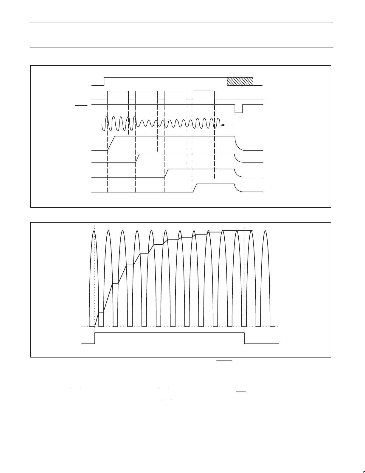
Burst Capture
Burst capture is controlled by the signal applied to the STROBE
input pin and an internal counter. The first pulse on the STROBE
input pin causes the A burst hold capacitor to be charged by the
charge pump. The capacitor charges for as long as the STROBE
input is High or until the capacitor voltage reaches the peak voltage
at the full wave rectifier output. On the falling edge of the STROBE
signal, the internal counter is incremented. The next 3 STROBE
pulses will charge the B, C, and D, hold capacitors respectively.
After the falling edge of the fourth strobe, the counter is reset to zero
and the burst capture can be repeated. The counter is also reset
when the RESET
The voltage level on each hold capacitor is amplified by a factor of
3.33 and summed with a 0.27V DC reference to create the A, B, C,
and D output signals. A 1.40 Vppd voltage at the DP/DN nodes will
result in 1.40 * 0.6 * 3.33 = 2.80V peak burst amplitude (i.e., servo
gain = 2.0). The MAXREF output pin is a nominal 3.2V and is
internally divided by 12 to create the DC baseline of 0.27V .
Either the normal or differentiated filter output may be selected for
full wave rectification for servo capture. If the Servo Mode Select
(SMS) bit in the Data Rate Register is 0 then the normal filter
outputs are used and if it is a 1, the differentiated filter outputs are
used. If the differentiated output is selected, the polarity of the
RDS/RDS
negative true. The magnitude of the captured voltage on the burst
hold capacitors is governed by setting of the 2-bit servo AGC DAC.
The AGC voltage can be programmed from 1.10 to 1.40 Vppd.
All four of the internal hold capacitors are discharged when the
RESET
input is driven Low. The RESET input overrides the
STROBE signal. STROBE and RESET
The maximum charge pump current can be selected as 40, 80, 120
or 160 µA by setting the servo burst charge current (SBCC) bits in
the Data Level Threshold register. The “Soft Landing” technique
reduces the charge pump current as the error between the voltage
on the hold capacitor and the full wave rectifier output becomes
smaller. This reduces the possibility of overcharging the capacitor
during the comparator’s propagation delay period.
A small leakage current is applied to the capacitor being charged
during each strobe period to make the captured voltage less
sensitive to noise and strobe timing. The magnitude of this current
is 1/450 of the charge current.
input transitions Low.
pulse will be positive true, otherwise RDS/RDS is
input pins. In addition to the A, B, C, D
are not gated with SG.
1997 JuL 15
18
Page 19
Philips Semiconductors Product specification
PRML Read Channel with PR4,
8/9 ENDEC, 4-Burst Servo
SG
STROBE
RESET
Burst A
Burst B
Burst C
Burst D
P32P4910B
SERVO DATA
Figure 13. Servo Capture Timing Diagram
Strobe
Figure 14. Servo Burst Acquisition (SG = RESET = 1)
Servo Timing Outputs
The dual level qualifier that was previously described is used to
generate the RDS/RDS
output pin pulses Low for each positive or negative servo peak that
is qualified by the dual level qualifier. The pulse width of RDS/RDS
may be selected as either 15 ns or 27 ns with the RDSPW bit in the
and PPOL timing signals. The RDS/RDS
SM00025
SM00036
Sample Loop Control Register . The PPOL output pin provides the
pulse polarity information for the qualified peaks, where PPOL=1 for
a positive peak and PPOL=0 for a negative peak. To reduce noise
propagation, the RDS/RDS
and PPOL outputs are only active in
servo mode.
1997 JuL 15
19
Page 20
Philips Semiconductors Product specification
PRML Read Channel with PR4,
8/9 ENDEC, 4-Burst Servo
DP/DN
RDS
PPOL
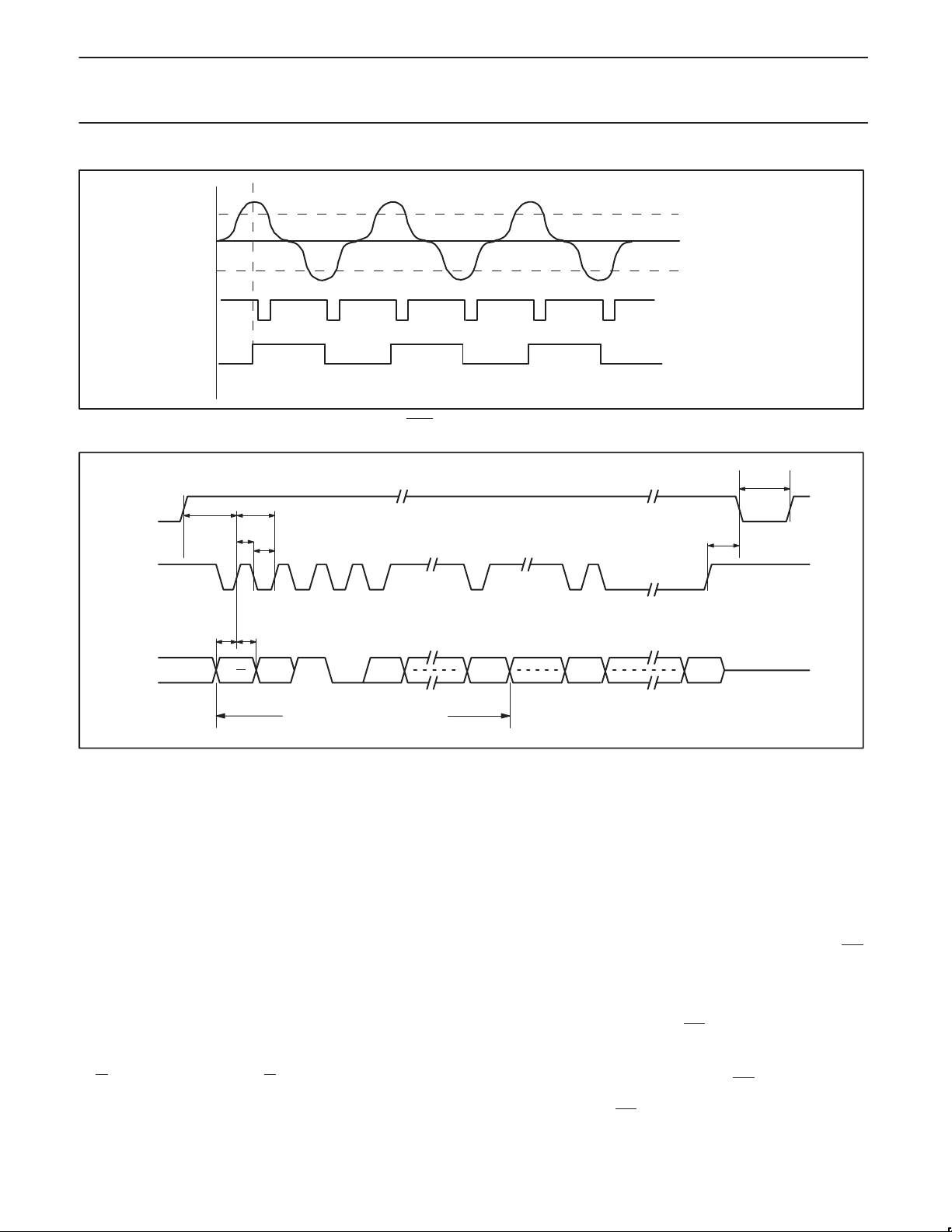
Figure 15. RDS/RDS and PPOL vs. DP/DN Relationship
SDEN
t
SENS
t
C
+ Threshold
(+LSth)
(–LSth)
– Threshold
P32P4910B
SM00037
t
SL
t
SCLK
SDATA
CKH
tDSt
R/W
t
CKL
DH
S0 S1 S2 A0 A3 D0 D7
COMPLETE REGISTER STRING ID
Figure 16. Serial Interface Timing
Serial Port Circuit
The serial port interface is used to program the P32P4910B’s
seventeen internal registers. The serial port is enabled for data
transfer when the Serial Data Enable (SDEN) pin is High (“1”).
SDEN must be asserted High prior to any transmission and it should
remain High until the completion of the transfer. At the end of each
transfer SDEN should be brought Low (“0”).
When SDEN is High, the data presented to the Serial Data (SDATA)
pin will be latched into the P32P4910B on each rising edge of the
Serial Clock (SCLK). Rising edges of SCLK should only occur when
the desired bit of address or data is being presented on the serial
data line. Serial data transmissions must occur in 16-bit packets. If
more than 16 rising edges of SCLK are received during the time that
SDEN is High, only the last 16 are considered valid. For all valid
transmissions, the data is latched into the internal register on the
falling edge of SDEN.
Each 16-bit transmission consists of a read/write control bit
(R/W
= “0” write to the register, R/W = “1” read back register
contents) followed by 3 device select bits, 4 address bits and eight
data bits. The device select and address bits select the internal
t
SENH
SM00174
register to be written to. The device select, address and data fields
are input LSB first, MSB last, where LSB is defined as Bit 0. The
three device select bits select the type of device on the Philips
Semiconductors serial bus to be communicated with and must be
set to S0 = 0 or 1 (depending on register to be selected), S1 = 1,
and S2 = 0 when communicating with the P32P4910B. Figure 16
shows the serial interface timing diagram.
Operating Modes
The fundamental operating modes of the P32P4910B are controlled
by the Servo Gate (SG), Read Gate (RG), and Write Gate (WG/WG
input pins. The exclusive assertion of any these inputs causes the
device to enter that mode. If none of these inputs is asserted, the
device is in the idle mode. If more than one of the inputs is
asserted, the mode is determined by the following hierarchy: SG
overrides RG which overrides WG/WG
takes effect immediately.
RG and SG are asynchronous inputs and may be initiated or
terminated at any position on the disk. WG/WG
asynchronous input, but should not be terminated prior to the last
output write data (WD/WD
) pulse.
. The mode that is overriding
is also an
)
1997 JuL 15
20
Page 21

Philips Semiconductors Product specification
PRML Read Channel with PR4,
8/9 ENDEC, 4-Burst Servo
MODE CONTROL
WG/WG RG DEVICE MODE DESCRIPTION
0/1 0 Idle Mode DS VCO locked to F
0/1 1 Data Read Mode DS PLL acquisition, adaptive equalizer training, code word boundary search and detect,
1/0 0 Data Write Mode Write mode preamble insertion and data write. DS VCO locked to F
1/0 1 Read Override RG overrides WG/WG which causes any write in progress to cease and Data Read
Idle Mode Operation
If SG, RG, and WG/WG
mode. When in idle mode, the Time Base Generator and the Data
Separator PLL are running and the Data Separator PLL is
phase-frequency locked to the TBG VCO output. The AGC,
continuous time filter, and pulse qualifiers are active but the outputs
of the pulse qualifiers are disabled. The continuous time filter is
using its programmed values for cutoff frequency and boost
determined by the data mode registers. The AGC operation is the
same as in the VCO preamble portion of a data read. Servo burst
capture is operational in idle mode but the filter and AGC settings
are for data reads and not for servo reads as would be the case if
the device was in servo mode. The RDS/RDS
are disabled in idle mode.
Servo Mode Operation
If SG is High, the device is in the servo mode. This mode is the
same as idle except that the filter cutoff and boost settings are
switched from those programmed for data read mode to those
programmed for servo mode, the AGC is switched to servo mode,
and the RDS/RDS
assertion of SG causes read mode, write mode, and the power
down register settings for the front end to be overridden.
Write Mode Operation
The P32P4910B supports three different write modes; Normal write
mode, direct write mode 1 and direct write mode 2. The direct write
modes require that either the direct write bit, bit 0 of the Control
Operating Register, or the DWR
require that the Data Separator be powered on. The active polarity
of write gate can be selected by programming the WGP bit in the
Control Operating Register. The PDWN
until all registers are properly loaded to prevent an illegal write
operation at power up.
Normal Write Mode
The P32P4910B is in the normal write mode if WG/WG
DWR
is High, and the direct write bit in the Control Operating
Register is Low. A minimum of one NRZ time period must elapse
after RG goes Low before WG/WG
Separator PLL is phase-frequency locked to the TBG VCO output in
this mode.
In normal write mode, the circuit first autogenerates the VCO sync
pattern, then optionally scrambles the incoming NRZ data from the
controller, encodes it into 8,9 GCR formatted data, precodes it,
precompensates it, feeds it to a write data toggle flip-flop, and
outputs it to the preamp for storage on the disk. When WG/WG
are not active, the P32P4910B is in idle
and PPOL and outputs are enabled. The
pin be active. All three write modes
input should be kept Low
can be set active. The Data
decode, sync byte detect, and NRZ data output. DS VCO switched from F
after preamble detect. RCLK gen. input switched from F
re-synchronized to RD at code word boundary detect. NRZ7–0 active.
synchronized to F
Mode to be entered.
and PPOL outputs
is active,
NRZ7–0 tri-stated.
TBG.
TBG
WD and WD active. NRZ7–0 = inputs.
TBG.
goes inactive, the WD/WD outputs remain enabled but the active
pull down current is reduced by a factor of 7 to reduce power
consumption and the write data flip-flop is reset to guarantee that
the WD/WD
In normal write operation, when the write gate (WG/WG) goes
active, the VCO sync field generation begins, which causes a
continuous “2T” pattern at the WD/WD
{(1,1,–1,–1,1,1,–1,–1...) in the write current domain}. The NRZ
inputs must be Low and must be held Low for the duration of the
VCO sync field generation. The minimum required sync field is
equivalent to 8 byte times.
The P32P4910B also allows the precoder to be preset when the first
training byte arrives at the precoder. With Control Operating Mode
Register 2’s bit 3 (TME) and bit 0 (PCFDIS) set to 0, the P32P4910B
allows presetting of the precoder. Bit 2 (PFSPOL) of the Control
Operating Mode Register #2 allows the precoder to be preset if
PFSPOL is set to 1 and reset if set to 0.
Training and Sync Byte Generation
The P32P4910B supports two modes of sync byte detection, single
byte and “or” dual byte, and two modes of training and sync byte
generation, manual and semi-automatic. The manual mode is
generally recommended because it can be used for either dual or
single sync byte detection and provides more flexibility in altering the
number of training bytes to be written. The semi-automatic mode
can only be used to generate an internally fixed number of training
bytes and a single sync byte, but saves controller state machine
space.
Manual Mode
In the manual mode, the device will continue to autogenerate the
sync field pattern until a 93H is latched at the NRZ interface, and
detected. The device encodes the 93H pattern and writes the result
as the training pattern.
For the single sync byte detection mode, a recommended minimum
of 5 bytes of 93H must be written to the NRZ interface to write the
5 byte equalizer training pattern. Next, the NRZ data must be
changed to 69H for 1 byte time to write the single sync byte.
For the dual sync byte detection mode, a recommended minimum of
4 bytes of 93H must be written to the NRZ interface to write the
minimum 5 byte equalizer training pattern. The NRZ data must then
be changed to 1FH for one byte time to write the first sync byte.
The NRZ data must then be changed to 93H for one byte time to
write a training/propagation byte. Next, the NRZ data must be
changed to 69H for one byte time to write the second sync byte.
outputs represent a zero state.
P32P4910B
TBG.
TBG
RCLK
to DS VCO. RCLK
outputs
to RD
1997 JuL 15
21
Page 22

Philips Semiconductors Product specification
PRML Read Channel with PR4,
8/9 ENDEC, 4-Burst Servo
GAP
NRZ DATA (WRITE) 00H 93H 69H
WG
VCO SYNC
FIELD
8 BYTES MIN. 4 BYTES MIN. 1 BYTE
Figure 17. Hard Sector Write Sequence – Dual Sync
GAP
NRZ DATA (WRITTEN BY 4910B)
NRZ DATA (WRITTEN TO 4910B) 00H
WG
VCO SYNC
FIELD
8 BYTES MIN. 5 BYTES 1 BYTE
00H 93H 69H
TRAINING
SEQUENCE
SYNC
BYTE#1
1FH
TRAINING
SEQUENCE
FFH FFH
TRAIN
BYTE
1 BYTE
93H
SYNC
BYTE
BYTE#2
1 BYTE
SYNC
SCRAMBLED AND ENCODED
SCRAMBLED AND ENCODED
USER DATA
USER DATA
P32P4910B
USER DATA
USER DATA
SM00038
USER DATA
Figure 18. Semi-Auto Sector Write Sequence Single Sync Only
Semi-Automatic Mode
In the semi-automatic mode, the device will continue to
autogenerate the sync field pattern until a FFH is latched at the NRZ
interface, and detected. The device then internally generates the
encoded the 93H pattern for 5 byte times and writes the result as the
training pattern. It then internally generates the encoded 69H
pattern for 1 byte time to write the single sync byte. To maintain
proper controller synchronization, the FFH should be presented at
the NRZ interface for a total of 6 byte times. Note that the
semi-automatic mode can only be used to write single sync byte
format and the training pattern length is fixed at 5. This mode is
useful if controller state machine space is extremely limited.
User Data
The user data must be presented at the NRZ interface immediately
following the last NRZ sync byte written. Finally, after the last byte
of user data has been clocked in, the WG/WG
must remain active
for a minimum of 16 NRZ bit times in byte-wide mode to ensure the
that the device is flushed of data (The delay is 21 NRZ bit times in
nibble mode). WG/WG
a maximum of 2 NRZ (RCLK) time periods after WG/WG
can then go inactive. WD/WD stops toggling
goes
inactive.
Direct Write Mode #1
In this direct write mode, the NRZ data from the byte-wide interface
bypasses the scrambler, the 8,9 encoder and the precoder, but is
precompensated before going to the write data flip-flop and then to
the WD/WD
output pins. The RCLK output is changed from 9 VCO
clock periods to 8 VCO clock periods with a 3/8 duty cycle. The
SM00168
purpose of routing the signal to the precomp circuit is to generate a
return to zero pulse every time a “1” occurs in the data so that the
write data flip-flop is toggled. WCLK is not required to latch the
byte-wide NRZ data into the NRZ interface since the data is latched
by an internal version of RCLK, but the NRZ data must be valid no
later than 12 ns after the rising edge of the RCLK output pin. Direct
write mode 1 is selected by setting the DW bit (bit 0) in the Control
Operating Register. and is entered when the WG/WG
input is active.
This mode is not valid when using the nibble NRZ interface. Note
that Direct Write Mode 2 will override Direct Write Mode 1.
Direct Write Mode #2
In this direct write mode, the data presented at the DWI/DWI
input
pins directly toggles the write data flip-flop which drives the WD/WD
output pins. No WCLK is required in this mode, and the WD/WD
output is not resynchronized. Direct write mode 2 is selected by
driving the DWR
input Low and is entered when the WG/WG input is
active. Note that the Direct Write Mode 2 will override Direct Write
Mode 1.
Data Read Mode Operation
Data read mode is initiated by setting the Read Gate (RG) input pin
High. This action causes the data synchronizer to begin acquisition
of the clock from the incoming VCO sync pattern. To achieve this,
the data synchronizer utilizes a fully integrated fast acquisition PLL
to accurately develop the sample clock. This PLL is normally locked
to the time base generator output, but when the Read Gate input
(RG) goes High, the PLL’s reference input is switched to the filtered
incoming read signal.
1997 JuL 15
22
Page 23

Philips Semiconductors Product specification
PRML Read Channel with PR4,
8/9 ENDEC, 4-Burst Servo
GAP
NRZ DATA
RG
SBD
HIGH Z 00H
Figure 19. Read Sequence – Dual or Single Sync Byte Modes
Acquisition of DS VCO Sync
When the Read Gate input is asserted, the read sequence is
initiated. At this time an internal counter begins counting the pulses
that are qualified by the dual level pulse qualifier given the polarity
changes of the incoming 1,1,–1,–1,1,1 read back pattern defined by
the VCO sync field. When the count reaches 4, the internal read
gate is asserted and the DS PLL input is switched from the TBG’s
VCO output to the sampled data input. This is also the point at
which the DS PLL’s phase detector is switched from the
phase-frequency detector to the decision directed phase detector.
The counter is also used to determine whether the selected sync
field count, SFC, has been achieved. When the counter reaches the
value specified by SFC, the data synchronizer PLL is assumed to be
locked and settled (VCO lock). Also at SFC, the phase detector
gain switch and the AGC mode switch occur. To allow for different
preamble lengths, the SFC can be set to 64, 80, 96 or 128 from the
Sample Loop Control Register. These values for the SFC may be
thought of as the number of code clock periods in the sync field, but
they actually represent twice the number of incoming polarity
changes required.
VCO Lock, PD Gain, AGC Mode Switch, and Code Word Boundary Detector Enable
At SFC, one of two phase tracking methods will be chosen
depending on the Enable Phase Detector Gain Switching (GS) bit in
the Control Operating Mode Register. When the GS bit is High, the
phase detector gain is reduced by a factor of 6 or 10 as dictated by
the GS_10 bit after the SFC count is reached. When the GS bit is
Low, no phase detector gain switching takes place.
Also after SFC, the AGC feedback will be switched from the
continuous time fullwave rectifier to sampled data feedback.
At SFC, the internal VCO lock signal activates the code word
boundary detection circuitry to define the proper decode boundaries.
Also, at count SFC, the RCLK generator source switches from the
TBG’s VCO output to the DS VCO clock signal which is phase
locked to the incoming read data samples. The DS VCO is
assumed locked to the incoming read samples at this point. At SFC
a maximum of 1 RCLK time period may occur for the RCLK
transition, however, no short duration glitches will occur. After the
code word detection circuitry finds the proper code word boundary,
the RCLK generator is again resynchronized to guarantee that the
RCLK is in sync with the data. The RCLK output will not glitch and
will not toggle during this RCLK generator resynchronization for up
to 2 byte times maximum.
Also at the code word boundary detect, the internal 9-bit code words
are allowed to pass to the ENDEC for decoding. This decoding will
occur until read gate is deasserted.
VCO SYNC FIELD
8 BYTES MIN.
P32P4910B
TRAIN
TRAINING
SEQUENCE
4 BYTES MIN.
00H
SYNC
BYTE#1
1 BYTE
00H
Adaptive Equalizer Training Sequence
Training Sequence for Single Sync Byte Mode
As was previously discussed, in a single sync byte type write
sequence, a minimum of 5 bytes of NRZ 93H and one byte of 69H
must be written between the end of the VCO sync field and the
beginning of the user data. The 5 bytes of 93H are 8,9 encoded and
precoded during write mode to produce the adaptive equalizer
training pattern. During read mode, the encoded 93H sequence
(1001 10011 read data sequence) and the encoded 69H are used to
adaptively train the inner two taps of the five tap transversal filter in
a zero forcing manner. The error at the filter output is integrated to
derive the tap weight multiplying coefficient, k
inner taps use the same k
time filter will be used for coarse equalization and that transversal
filter will be used adaptively for fine tuning. This will reduce km’s
range and accuracy requirements. Since there are encoded user
data patterns that will not produce an equalizer correction error, an
equalization hold during data mode can be selected from the
Sample Loop Control Register . If the equalizer is programmed to
adapt only during the training sequence, the sync byte detect signal
is used to hold the k
active during user data, the equalizer loop gain will be reduced by 7.
The loop’s integration time constant is made inversely proportional
to the selected data rate.
The k
coefficient can be held at the present instantaneous value
m1
by asserting the EQHOLD input. If EQHOLD is asserted, the k
value will not be changed by either exiting read mode, subsequent
training patterns, or by subsequent data patterns. When EQHOLD
is deasserted, the equalizer will resume its normally programmed
functionality. The k
for up to 10 ms to make the number of code periods required for
acquisition data rate independent.
Training Sequence for Dual Sync Byte Mode
The adaptive equalizer training used for the dual sync byte detection
mode is the same as that used in the single sync byte mode except
that the adaptation occurs over the 4 encoded 93H bytes, sync byte
1 (1FH), another 93H and sync byte 2 (69H). This occurs because
the Sync Byte Detect (SBD
adaptation is enabled only during the training sequence. The
number of consecutive 93H training bytes may be reduced in dual
sync byte mode because the sync byte 1 has been chosen to have
the same training properties as the 93H training byte.
Sync Byte Detect and NRZ Output
The P32P4910B implements a dual “OR” type sync byte detection
which offers increased sync byte detection capability while
maintaining backward compatibility with the single sync byte format
SYNC
SCRAMBLED AND ENCODED
BYTE#2
BYTE
1 BYTE
1 BYTE
69H
00H
. It is anticipated that the continuous
m1
value. After the training pattern, if the loop is
m1
value can be held with reasonable accuracy
m1
USER DATA
USER DATA
m1
. Both of these
) is what disables the adaptation if
SM00175
m1
1997 JuL 15
23
Page 24

Philips Semiconductors Product specification
PRML Read Channel with PR4,
8/9 ENDEC, 4-Burst Servo
and detection. The two bytes of the dual sync byte are separated by
a training byte to allow for Viterbi error propagation that may be
caused by an error in the first sync byte. The training byte 93H was
chosen to provide the adaptive equalizer an ideal training signal.
As the read data is 8,9 decoded, it is compared to one of two
internally fixed sync bytes (1FH or 69H). If the 1FH byte is found,
the SBD
output will go Low 18 code clocks (2 byte times) later and
the 69H byte will be the first non-zero byte presented at the NRZ
interface. If a match of the 69H byte is the first found, the sync byte
detect (SBD
was held Low, is changed to 69H. The next byte presented on the
NRZ outputs is the first byte of user data. SBD
NRZ data will continue to be presented at the NRZ interface until the
read gate is deasserted at which point SBD
outputs go to a High impedance state.
) pin goes Low and the NRZ output data that until now
will remain Low and
goes High and the NRZ
SFC
RG
P32P4910B
Surface Defect Scan Mode
The P32P4910B helps check for media defects using the surface
defect scan mode. In order to use this mode the part must have the
byte-wide interface enabled. In write mode, all zeros are presented
(written) at the NRZ interface. When this pattern is to be read back,
bit 7 (DSE bit) of the N Counter Register is enabled which enables
the surface defect scan mode. The survival sequence register must
also be turned off (BYPSR bit). In this mode, SBD
Low at SFC. The NRZ7 pin is monitored. If no defect occurs, the
NRZ7 pin will stay Low. If a defect occurs, the NRZ7 pin will
transition High on the falling edge of RCLK and stay high as long as
the defect is present. It transitions back Low on the next falling edge
of RCLK when the defect is not present.
will transition
SBD
RCLK
NRZ7
DEFECT
SM00002
Figure 20. Surface Defect Scan Mode
1997 JuL 15
24
Page 25

Philips Semiconductors Product specification
PRML Read Channel with PR4,
8/9 ENDEC, 4-Burst Servo
Power Down Operation
The power management modes of the P32P4910B are determined
by the states of the Power Down Register bits and the PDWN
SG inputs. The individual sections of the chip can be powered down
or up using the Power Down Register. A High level in a Power
Down Register bit disables that section of the circuit. The power
down information from the Power Down Register takes effect
immediately after the SDEN pin goes Low.
When the PDWN
mode regardless of the power down register settings or the state of
the SG input.
When PDWN
qualifier circuits (front end) to be active by overriding the front end
register bit. The back end power down register bits, which include
the Data Separator and Time Base Generator are not affected by
the SG input.
The serial port is active in all power down modes.
input is Low, the chip goes into full power down
is High, SG will force the AGC, filter, and pulse
and
Table 3. Dynamic Power Management when Invoked by CT<7:6>
The time to restart from a full power down is dependent on the PLL
loop filter and the data rate.
The truth table for the various modes of operation is shown below:
SG, PDWN:
Front End ON OFF R OFF
Data Separator R OFF R OFF
Time Base Generator R OFF R OFF
Serial Port ON ON ON ON
R = Controlled by register bit.
(Register bit =1 turns circuits OFF,
Bits 6 and 7 of the Control Mode Register (CT) allow for dynamic
power management which is transparent to the user. Bit 7 controls
read-mode circuits and bit 6 controls write-mode circuits. The
following table indicates which circuits are affected by dynamic
power management:
P32P4910B
1,1 1,0 0,1 0,0
Register bit = 0 turns circuits ON)
SG, RG, WG
0,0,0
IDLE
Qualifier CT<7:6> OFF ON ON UNTIL VCOLOCK OFF
SDP except PLL CT<7> OFF OFF ON OFF
Write Precomp CT<6> ON OFF OFF ON
Other write circuitry CT<6> OFF OFF OFF ON
Thermal Asperity Detection and Suppression
A thermal asperity (TA) event appears to the read channel as a
sudden (10’s of ns) baseline shift of the incoming read signal
followed by an exponential (300 to 500 ns time constant) decay.
These events always occur in the positive direction. The magnitude
of an asperity is defined as follows:
100% TA base to peak
TA% +
The thermal asperity detection (TAD) and suppression circuitry in
the Philips 32P4910B is designed to accomodate TA magnitudes as
large as 500% while keeping the burst error length less than five
bytes.
Thermal Asperity Circuit
The thermal asperity detector monitors the signal at the filter’s
low-pass output pins (DP/DN) with a threshold comparator. This
comparator is very similar to the comparator used for level pulse
qualification. Under normal conditions, the signal at this point should
be about 1.4 Vpp. A thermal asperity will cause a sudden increase in
the baseline voltage which will trip the threshold comparator. The
nominal base to peak
+ 100%
Vta
Vs
1,X,X
SERVO
threshold setting is programmable from +0.83 Vpk to +1.6 Vpk with
4 bits of resolution. This corresponds to a percent threshold setting
from 118% to 229% of the nominal zero to peak voltage swing.
When the signal crosses this positive threshold, the TAD signal is
asserted. When the signal falls below –0.35 Vpk, the TAD signal is
reset.
In order to keep the detection circuit from triggering on the normal
AGC transient response, the detection circuit is held reset whenever
the Low-Z or fast recovery modes are activated.
The user should program the TAth Register to set the positive
detection threshold. It should be set high enough to avoid false
triggering. The negative reset threshold of –0.35 Vpk is not
adjustable.
The internal TA detect, error flag, and external TA detect signals are
multiplexed onto the RDS, PPOL, TAD, and EFLAG pins. The
following table summarizes how these pins are mapped in all modes
of operation. When the TAD pin is enabled as an input, the internal
TA detect circuit is disabled. The TA suppression methods will be
triggered by a rising edge at the TAD pin.
0,1,X
READ
0,0,1
WRITE
1997 JuL 15
25
Page 26
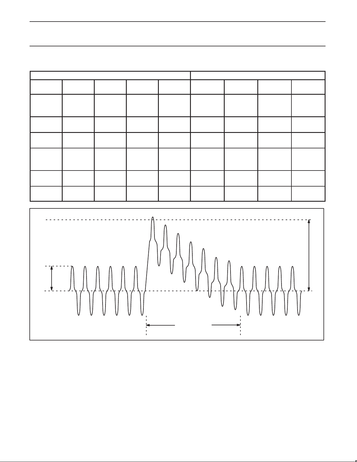
Philips Semiconductors Product specification
PRML Read Channel with PR4,
8/9 ENDEC, 4-Burst Servo
Table 4. Thermal Asperity Input/Output Pin Control
Control Bits and Mode Control Pins TA Pin Functionality
RDSMUX TAIO TADE SG RG RDS PPOL
0
0
0
0
0
0
0
1
1
1
1
1
1
1
0
0
0
0
0
1
1
0
0
0
0
0
1
1
0
0
0
1
1
X
X
0
0
0
1
1
X
X
0
0
1
0
1
0
1
0
0
1
0
1
0
1
0
1
X
X
X
X
X
0
1
X
X
X
X
X
held low
T AD out
RD
T AD out
RD
held low
RD
held low
held low
RD
held low
RD
held low
RD
held low
held low
held low
held low
EFLAG
EFLAG
PPOL
EFLAG
PPOL
EFLAG
PPOL
PPOL
PPOL
PPOL
P32P4910B
TAD
(32P4910BP)
held low
T AD out
T AD out
T AD out
T AD out
T AD in
T AD in
held low
T AD out
T AD out
T AD out
T AD out
T AD in
T AD in
EFLAG
(32P4910BP)
EFLAG
EFLAG
EFLAG
EFLAG
EFLAG
EFLAG
EFLAG
EFLAG
EFLAG
EFLAG
EFLAG
EFLAG
EFLAG
EFLAG
Vs
Figure 21. Thermal Asperity Occurence
Thermal Asperity Suppression Circuit
NRZ errors caused by thermal asperity events are unavoidable. The
suppression measures listed below are intended to limit the duration
of the errors at the NRZ output. The suppression methods can only
be activated when in read mode (RG = High) or servo mode
Vta
4 ms
SM00163
(SG=High). If an asperity occurs within 4 ms before the leading edge
of RG, the suppression measures will go active when RG goes high
and remain active for the indicated duration from the leading edge of
TAD. At power-up, all the suppression features will be disabled and
must be enabled via the serial port.
1997 JuL 15
26
Page 27
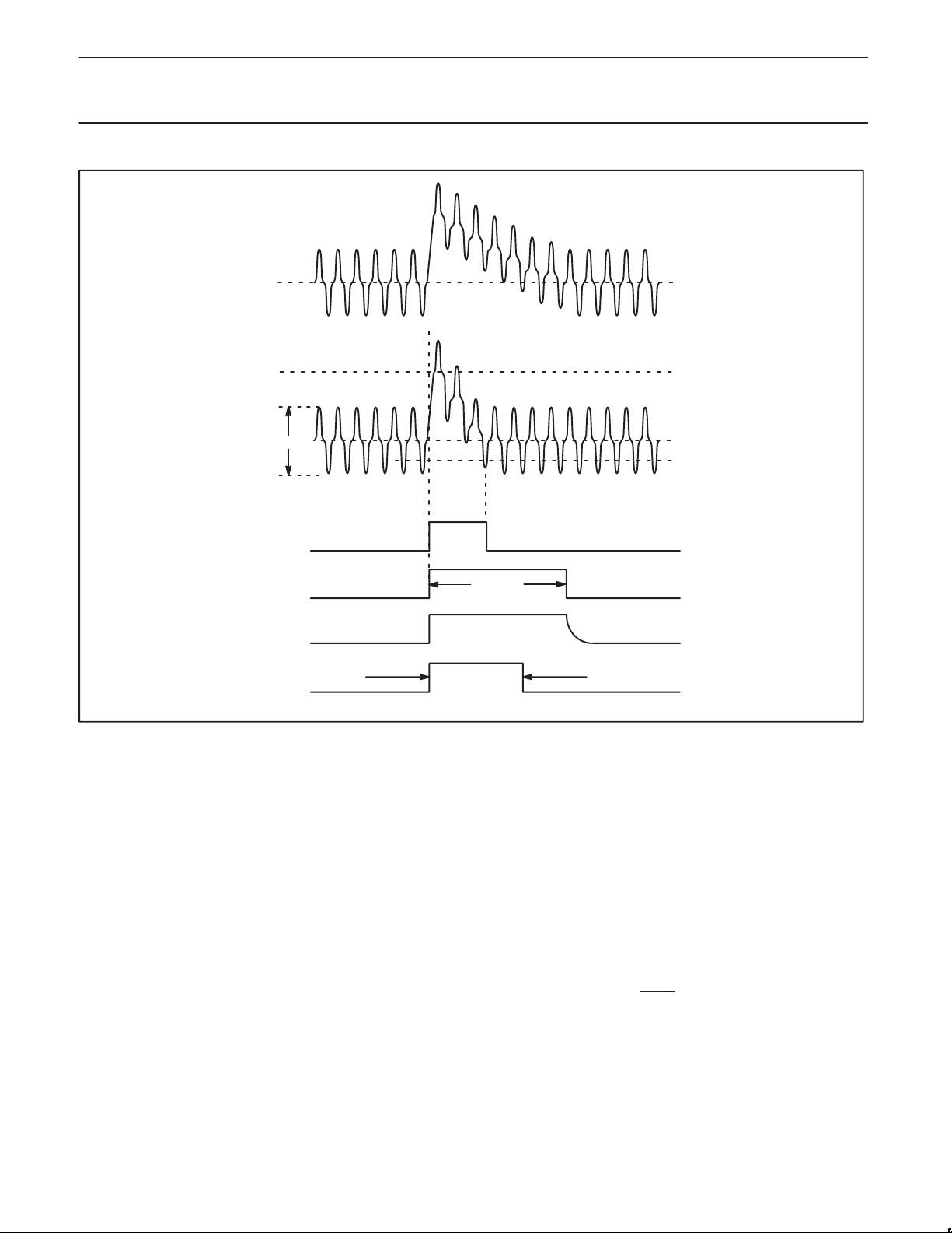
Philips Semiconductors Product specification
PRML Read Channel with PR4,
8/9 ENDEC, 4-Burst Servo
Preamp
Output
Filter DP/DN
Output
1.4 Vpp
P32P4910B
+ TA Threshold
–TA Threshold
TA Detect
Dynamic Hi-Y
VIA+/VIA– Input Y
AGC/PLL Hold
Figure 22. Thermal Asperity Timing
Dynamic Hi-Y
When the TAD signal goes active, the input conductance of the
VGA amplifier can be quickly set to a higher value. This allows the
high-pass conrner at the VIA+/VIA– pins to be modulated. If the
AC coupling capacitor at the VIA+ pin is C, and Yin is the
differential input conductance between VIA+ and VIA–,
then Fhp = 2 * Yin/(2*p*C). By moving Fhp to a higher frequency,
the low frequency characteristic of the thermal asperity can be
quickly attenuated. The input admittance will have a fast turn on
(<100 ns), slow turn off (about 1 ms) characteristic to minimize
glitches going into the AGC amplifier. The modulated Fhp frequency
should be proportional to the NRZ data rate. Three serial port bits
allow eight different values of input admittance to be programmed
for Hi-Y in read mode.
The duration of the dynamic Hi-Y state will be 4 ms following the
leading edge of T AD. This time period is not adjustable. A static Hi-Y
mode is also available in which the Hi-Y condition will be asserted
whenever SG is Low. This mode should prove useful in a “re-try”
mode of thermal asperity suppression. The dynamic Hi-Y correction
can be independently programmed to activate in servo and/or read
mode. If the servo mode is selected, the Hi-Y condition at the input
will correspond to YIN<2:0> = 000b.
4 ms
0.25 – 2 ms
AGC/PLL Hold
The signal at DP/DN should not be used for adaptive AGC,
equalization, timing extraction , or offset correction until the proper
baseline has been restored. Therefore, all of these functions may be
suspended for a programmable time period when a thermal asperity
is detected. The hold time may be programmed from 0.25 to 2 ms
with a 0.25 us resolution. The user should program this time period
to match the signal recovery time in the dynamic Hi-Y mode. If this
time period is set too long, there is a risk of losing the proper timing
relationship in the PLL. An option is provided which allows the
internal error flag signal instead of the internal one-shot to turn off
the PLL hold.
The AGC and AC coupling hold function are enabled by a single bit
in the serial port. The AGC hold function itself can be manually
controlled by asserting the HOLD
has a separate enable bit in the serial port. The PLL and equalizer
hold function can be manually controlled by asserting the
EQ/PLLHOLD input pin. A serial port bit is provided to force
equalizer hold following sync byte detect.
input pin. the PLL hold function
SM00164
1997 JuL 15
27
Page 28

Philips Semiconductors Product specification
PRML Read Channel with PR4,
8/9 ENDEC, 4-Burst Servo
Error Flag
A thermal asperity event always has a positive polarity since an MR
head has a positive temperature coefficient of resistance. The error
flag circuitry monitors the level slicer output from the sampled data
processor. A run of five or six positive “1” samples indicates the
occurrence of an asperity. This sets an internal error flag which
marks the corresponding NRZ data as being corrupted. The circuit
looks for a negative “1” to start the process of resetting the error
flag. When a negative “1” is detected, an internal counter begins to
count six internal clock periods. If a run of three or four positive “1”
samples occurs during this count down, the counter starts over. If
the counter is able to reach six without being restarted, the error flag
is allowed to reset itself. The external EFLAG pin will be asserted to
mark corrupt NRZ data. This signal should aid the error correction
circuitry in recovering data during a thermal asperity event. Since
P32P4910B
the error flag monitoring circuit does not impact the normal signal
path in any way, no provision is made to disable this function.
Applying Thermal Asperity Detection and Suppression
The TA detection threshold should be set low enough to flag any
asperity which can cause an error burst longer than the ECC can
handle. When an asperity is detected, it is recommended that
dynamic Hi-Y, AGC/PLLHOLD, and error flag monitoring be applied.
This will give the best probability of “on-the-fly” asperity correction.
The duration of AGC/PLLHOLD should be just long enough to
prevent corrupt data from disturbing any of these control loops. The
static Hi-Y mode is included to allow asperity correction on a “retry”
basis. The user must also take care that the proper signal polarities
are maintained throughout the read channel so that thermal
asperities appear as positive displacements.
1997 JuL 15
28
Page 29
Philips Semiconductors Product specification
PRML Read Channel with PR4,
8/9 ENDEC, 4-Burst Servo
REGISTER DESCRIPTIONS
Serial Port Register Descriptions
Complete Register String ID A3 A2 A1 A0 S2 S1 S0 R/W
Power Down Register (PD) 0 0 0 0 0 1 0 0 04H
Bits 7–6 TPC/
D1–0
Test point C/D/E control (TME = 0)
TPC+/TPC– TPD+/TPD– TPE
0X = disabled disabled disabled
1X = DP/DNout CP/CNout disabled SG = 1
1X = disabled disabled disabled SG = 0
Test Point C/D/E Control (TME = 1)
TPC+/TPC– TPD+/TPD– TPE (AGCSEL=0) TPE(AGSEL=1)
00* = Servo mode calibration
01 = DP/DN CP/CN full wave Low-Z oneshot
rectifier out
as input mode to qualifiers, etc.
10 = DP/DN CP/CN full wave fastrec
rectifier out oneshot
output mode from filter/offset canceller
11 = filter filter full wave ultra fast
bypass bypass rectifier out decay ctrl.
P32P4910B
Bits 5–4 AT OSEL Output select for ATO test point
Bit 3 ACCPL Internal AC coupling enable/disable (TME = 0)
Bit 2 TB Time Base Generator power down
Bit 1 DS Data Separator power down
Bit 0 PD AGC, Filter, Pulse Detector, and Servo power down
* Servo calibration mode enabled, strobing must occur for operation.
Data Filter Cutoff Register (FC) 0 0 0 1 0 1 0 0 14H
Bit 7 3TAPEN 3 T ap equalizer enable
00 = MAXREF/2
01 = DAC output enabled DAC test mode
10 = Amplitude Asymmetry Monitor output (QASYM) selected
11 = Channel Equalization Monitor output (Q) selected
0 = Internal AC coupling, AGC switched to sample mode at SFC
1 = Inte r nal AC coupling, AGC is always in continuous mode
Internal AC coupling enable/disable (TME = 1)
0 = Internal AC coupling is enabled, AGC as per last TME = 0 state
1 = Internal AC coupling is disabled
0 = power up
1 = power down
0 = power up
1 = power down
0 = power up
1 = power down
0 = enable 5 tap equalizer (Normal operation)
1 = enable only 3 tap equalizer (4901 mode)
1997 JuL 15
Bits 6–0 FC6–0 Filter cutoff frequency setting in non-servo mode
ƒc (MHz) = 0.301 * FC – 1.142 44 ≤ FC ≤ 117
29
dec
Page 30
Philips Semiconductors Product specification
(VDT)
PRML Read Channel with PR4,
8/9 ENDEC, 4-Burst Servo
Serial Port Register Descriptions (Continued)
Complete Register String ID A3 A2 A1 A0 S2 S1 S0 R/W
Servo Filter Cutoff Register (FCS) 0 0 1 0 0 1 0 0 24H
Bit 7 PDM Servo Peak Detector Mode
Bits 6–0 FCS6–0 Filter cutoff frequency setting in servo mode
Data Filter Boost Register (FB) 0 0 1 1 0 1 0 0 34H
Bit 7 LZTC Non Low-Z vs. Low-Z time constant
Bits 6–0 FB6–0 Filter boost setting in data mode
Servo Filter Boost Register (FBS) 0 1 0 0 0 1 0 0 44H
Bits 7–6 FBS 1–0 Filter boost setting in servo mode
Bits 5–0 FGD5–0 Filter Group Delay ∆ % In all modes
Viterbi Detector Threshold Register
0 1 0 1 0 1 0 0 54H
Bit 7 BYPSR Survival Sequence Register Bypass/Write Precode Bypass
0 = Window Qualifier
1 = Hysteresis Qualifier
ƒc (MHz) = 0.277 * FC + 0.08 14 ≤ FC ≤ 43
0 = 15:1
1 = 5:1
Boost (dB) = 20 * log[0.021848 * FB + 0.000046 * FB * FC + 1]
0 ≤ FB ≤ 127
00 = 0 dB
01 = 2 dB
10 = 4 dB
11 = 6 dB
Group Delay ∆ % = 0.9783 * (FGD 4–0) – 0.665,
where FGD5 = 1 is positive, 0 is negative
0 ≤ FGD ≤ 31
0 = bypass disabled (normal operation)
1 = bypass enabled
dec
dec
P32P4910B
dec
Bits 6–0 VD6–0 Viterbi qualification threshold voltage
Data Level Threshold Register (LD) 0 1 1 0 0 1 0 0 64H
BIts 7–6 SBCC1–0 Initial Servo Charge Pump Current
Bits 5–0 LD5–0 Data level qualification threshold voltage
1997 JuL 15
Vth (mV) = 6.61*VD–1.7
45 ≤ VD ≤ 127
00 = 40 µA
01 = 80 µA
10 = 120 µA
11 = 160 µA
if WP/LT Register
Prior to SFC : Lth (mV) = 9.73 * LD + 15.9
After SFC : Lth (mV) = 7.44 * LD
16 ≤ LD ≤ 63
if WP/LT Register : ALE = 1 (Adaptive levels)
After SFC : Lth (%) = 1.574 * LD
30
dec
:
ALE = 0 (Fixed levels)
dec
Page 31
Philips Semiconductors Product specification
(LDS)
PRML Read Channel with PR4,
8/9 ENDEC, 4-Burst Servo
Serial Port Register Descriptions (Continued)
Complete Register String ID R/WS0S1S2A0A1A2A3
Servo Level Threshold Register
Control Test Mode Register (CT) 1 0 0 0 0 1 0 0 84H
0 1 1 1 0 1 0 0 74H
Bits 7–6 SAGC
LVL1–0
Bits 5–0 LDS5–0 Servo level qualification threshold voltage
Bit 7 PME/EFR Power Management Enable (TME = 0)
Servo mode AGC level control
00 = 1.40 Vppd
01 = 1.30 Vppd
10 = 1.20 Vppd
11 = 1.10 Vppd
LSth (mV) = 9.73 * LDS + 15.9
0 = power management off
1 = enable power management
Sample clock source
0 = sample clock is from the DS VCO, normal operation
1 = sample clock is from the TBG output, a test mode
P32P4910B
Bit 6 BPME/
ECP
Bits 5–3 TP3–1 Multiplexed test point selection
Back-End Power management Enable (TME=0)
0 = back-end power management off
1 = back-end power managment enabled
Factory reserved bit, (TME=1)
must be set to 0 in application (enables charge pump)
1997 JuL 15
31
Page 32
Philips Semiconductors Product specification
(Continued)
PRML Read Channel with PR4,
8/9 ENDEC, 4-Burst Servo
TP3 TP2 TP1 Function TPA+, TPA– TPB+, TPB–
0 0 0 Test Points Off high impedance high impedance
0 0 1 Survival Out/Inputs SSOUT A, B (sngl) SSIN A+, A– (sngl),
0 1 0 Eq Cont/Phase Det Equalizer Control (diff) Phase Detect Out (dif f),
0 1 1 Viterbi Survival Inputs SSIN B+,B– (sngl) SSIN A+, A– (sngl),
1 0 0 Equalizer Outputs Equalizer A (diff) Equalizer B (diff)
1 0 1 EQ out/Survival Inputs Equalizer A (diff) SSIN A+, A– (sngl)
1 1 0 EQ out/Survival Outputs Equalizer A, B (sngl) SSOUT A, B (sngl)
1 1 1 EQ out/VCO/2 Equalizer A, B (sngl) DS VCO/2 (diff) for RG = 1
EQ out/TBG outputs Equalizer A, B (sngl) TBG out (diff) for RG = 0
Control Test Mode Register (CT)
1 0 0 0 0 1 0 0 84H
Bit 2 RCK2X/V
RDT
Bit 1 DT 0 = not in pump down test mode
Bit 0 TT/UT Training T ermination
Enable double RCLK drive (TME = 0) at Byte wide NRZ interface
0 = RCLK drive at 1x
1 = RCLK drive at 2x
Enable VRDT input (TME = 1)
0 = Viterbi survival outputs to the data decoder, normal use
1 = digital input to the data decoder, used in testing only
1 = digital input to the data decoder, for test only
Found sync byte (TME = 1)
0 = terminate training when SBD
1 = terminate training 4 bytes after framing
Enable TBG pump up (TME = 1)
0 = not in pump up test mode
1 = continuous pump up, for test use only
FLTR1+ sources current; FLTR1– sinks current
goes Low
P32P4910B
1997 JuL 15
32
Page 33
Philips Semiconductors Product specification
PRML Read Channel with PR4,
8/9 ENDEC, 4-Burst Servo
Serial Port Register Descriptions (Continued)
Complete Register String ID A3 A2 A1 A0 S2 S1 S0 R/W
N Counter Register (N) 1 0 0 1 0 1 0 0 94H
Bit 7 DSE Defect Scan Enable
Bits 6–0 N6–0 N Counter
M Counter Register (M) 1 0 1 0 0 1 0 0 A4H
Bits 7–0 M7–0 M Counter
Data Rate Register (DR) 1 0 1 1 0 1 0 0 B4H
Bits 7 SMS Servo Mode Select
Bits 6–0 DR6–0 F
0 = normal operation
1 = defect scan mode enabled
2 ≤ N ≤ 127
2 ≤ M ≤ 255
= FREF * [(M+1) ÷ (N+1)]
F
TBG
0 = Capture uses normal filter output and RDS is active Low
(normal operation)
1 = Capture uses differentiated filter output and RDS is active High
(MHz) = 9/8 Data Rate = 1.143 * DR + 4.986 for
VCO
RR = 10 kΩ
(MHz) = 9/8 Data Rate = 0.948 * DR + 1.831 for
F
VCO
RR = 12.1 kΩ
37 ≤ DR ≤ 127
P32P4910B
1997 JuL 15
33
Page 34
Philips Semiconductors Product specification
Constant Register (WPLT)
PRML Read Channel with PR4,
8/9 ENDEC, 4-Burst Servo
Serial Port Register Definitions (Continued)
Complete Register ID String A3 A2 A1 A0 S2 S1 S0 R/W
Write Precomp / Level Threshold Time
WPC3 WPC2 WPC1 WPC0 Write Precomp Magnitude
0 0 0 0 No precomp
0 0 0 1 2.1% code period shift
0 0 1 0 4.2% code period shift
0 0 1 1 6.3% code period shift
0 1 0 0 8.4% code period shift
0 1 0 1 10.5% code period shift
0 1 1 0 12.6% code period shift
0 1 1 1 14.7% code period shift
1 0 0 0 16.8% code period shift
1 0 0 1 18.9% code period shift
1 0 1 0 21.0% code period shift
1 0 1 1 23.1% code period shift
1 1 0 0 25.2% code period shift
1 1 0 1 27.3% code period shift
1 1 1 0 29.4% code period shift
1 1 1 1 31.5% code period shift
1 1 0 0 0 1 0 0 C4H
Bits 7–6 TC2–1 Adaptive Level qualification threshold time constant for Decision
Bit 5 ALE Enable adaptive level qualification in Decision Directed Phase Detector
Bit 4 FREZQ Freeze Channel Quality Factor and Asymmetry Factor at Sync Byte
Bits 3–0 WPC3–0 Write Precomp setting
Directed Phase Detector. (Valid After SFC)
TC2
0
0
1
1
0 = fixed level qualification
1 = adaptive mode
Detect
0 = Update during read
1 = Freeze at SBD
TC1
0
1
0
1
Time Constant
200 ns
400 ns
600 ns
800 ns
P32P4910B
1997 JuL 15
34
Page 35
Philips Semiconductors Product specification
PRML Read Channel with PR4,
8/9 ENDEC, 4-Burst Servo
Serial Port Register Definitions (Continued)
Complete Register ID String A3 A2 A1 A0 S2 S1 S0 R/W
Control Operating Register (CM1) 1 1 0 1 0 1 0 0 D4H
Bit 7 AUTOTR Enables Semi-Automatic training and sync byte generation
0 = disabled (normal operation)
1 = enabled (single sync byte only)
Bit 6 AGCSEL Selects AGC control mode
0 = Direct mode i.e., external control signals must be provided
1 = Timed mode i.e., control provided by one shot timing
from SG and WG/WG
Bit 5 WGP Write gate polarity
0 = active High, (normal operation)
1 = active Low
Bit 4 NIB Enable Nibble interface (RCLK Driver Mode)
0 = Nibble interface disabled, i.e., byte-wide interface enabled
1 = Nibble (NRZ3–0) interface enabled
Bit 3 BT Bypass Time Base Generator
0 = data synchronizer reference frequency is TBG output,
(normal operation)
1 = data synchronizer reference frequency is FREF input
Bit 2 SD Disable Data Scrambler/Descrambler
0 = enabled, (normal operation)
1 = disabled
P32P4910B
Bit 1 GS DS Phase Detector gain switching
Bit 0 DW Enable Direct Write From Byte-wide NRZ (Bypasses scrambler and
0 = enabled, (normal operation)
1 = disabled
ENDEC)
0 = disabled (normal operation)
1 = enabled
1997 JuL 15
35
Page 36

Philips Semiconductors Product specification
(SLC)
(DRC)
PRML Read Channel with PR4,
8/9 ENDEC, 4-Burst Servo
Serial Port Register Definitions (Continued)
Complete Register ID String A3 A2 A1 A0 S2 S1 S0 R/W
Sample Loop Control Register
Damping Ratio Control Register
1 1 1 0 0 1 0 0 E4H
Bit 7 RDSPW RDS output pulse width
Bits 6–5 SFC1–0 Sync Field Count
SFC1
0
0
1
1
Bit 4 AEGS Adaptive Equalizer Loop time constant shift
Bit 3 AED Enable Adaptive Equalizer on Data Field
Bit 2 AEE Enable Adaptive Equalizer
Bits 1–0 AGC1–0 AGC charge pump current in Sampled AGC mode
1 1 1 1 0 1 0 0 F4H
Bit 7 GS_10 Data separator PLL gain shift factor
SFC0
0
1
0
1
0 = 15 ns
1 = 27 ns
Sync Field Count (code clocks)
64
80
96
128
0 = equalizer loop time constant same in preamble and data fields
1 = equalizer loop time constant is increased to 7X in the data field
relative to the preamble field, i.e. loop gain is reduced to 1/7
0 = adaptive equalizer disabled after preamble field
1 = adaptive equalizer in use after preamble field,
if AEE bit = 1
0 = adaptive equalizer disabled
1 = adaptive equalizer enabled for use in preamble field, and after the
preamble field if AED bit = 1
AGC charge/discharge current (µA) = 2.66 * AGC * DR/RR (kΩ)
37 ≤ DR ≤ 127, RR = 10 kΩ e.g., for DR = 100 and
AGC=10 =2
0 = 6
1 = 10
charge pump current = 53 µA
dec
P32P4910B
1997 JuL 15
Bits 6–0 D6–0 Damping amplifier gain A = D * (0.8 / 127)
Damping Ratio =
36
A KVCO 0.25
2w
n
Page 37

Philips Semiconductors Product specification
(CM2)
PRML Read Channel with PR4,
8/9 ENDEC, 4-Burst Servo
Serial Port Register Definitions (Continued)
Complete Register ID String A3 A2 A1 A0 S2 S1 S0 R/W
Control Operating Mode Register 2
0 0 0 0 0 1 1 0 06H
Bits 7–4 KM3–0 Equalizer outer tap coefficient k
km2 = 0.0168 * KM (KM is in 2’s compliment)
0111 = +0.1 17
0110 = +0.101
0101 = +0.0840
0100 = +0.0672
0011 = +0.0504
0010 = +0.0336
0001 = +0.0168
0000 = 0
1111 = –0.0168
1110 = –0.0336
1101 = –0.0504
1100 = –0.0672
1011 = –0.0840
1010 = –0.1010
1001 = –0.1170
1000 = –0.1350
m2
P32P4910B
Bit 3 TME Test Mode Enable
0 = TPC and TPD active when SG = 1 and bit 7 of Power
Down Control Register is 1
1 = TPC and TPD as set by bits 6 and 7 of the Power Down
Control Register
Bit 2 PFSPOL Precoder Force State Polarity
0 = Precoder state set to 0
1 = Precoder state set to 1
Bits 1–0 QTC1–0 Qasym and Q Time Constant Control (TME = 1)
Qasym Q
00 = 100 ns 50 ns
01 = 200 ns 100 ns
10 = 400 ns 200 ns
11 = 800 ns 400 ns
Bit 0 PFSDIS Precoder Force State Disabled (TME = 0)
0 = Precoder initialization enabled
1 = Precoder initialization disabled
1997 JuL 15
37
Page 38
Philips Semiconductors Product specification
PRML Read Channel with PR4,
8/9 ENDEC, 4-Burst Servo
Serial Port Register Definitions (Continued)
Complete Register ID String A3 A2 A1 A0 S2 S1 S0 R/W
Thermal Asperity Register 1 0 0 0 1 0 1 1 0 16H
Bit 7 SVHY Hi-Y in Servo Mode
0= deactivates Hi-Y on TA detect in servo mode
1 = activate Hi-Y on TA detect in servo mode for 4 ms
Bit 6 SELERA Selection of PLL Hold Termination
0= internal time control of PLL hold only
1 = falling edge at interval EFLAG deasserts PLL hold
Bit 5 PLLHE PLL Hold Enable
0 = normal operation
1 = enable PLL hold over thermal asperity
Bit 4 AGCHE AGC Hold Enable
0 = normal operation
1 = enable AGC hold over thermal asperity
Bits 3–0 TATH Thermal Asperity Threshold Voltage Control
Threshold voltage (mV) = 41.6 * TATH + 825,
0 TATH 15
P32P4910B
Thermal Asperity Register 2 0 0 1 0 0 1 1 0 26H
Bit 7 HYED Hi-Y Enable, Dynamic Mode
Bit 6 HYES Hi-Y Enable, Static Mode
Bits 5–3 YIN Dynamic High Admittance Control
Bits 2–0 TATMR PLL/AGC Hold Time Duration During Thermal Asperity
0= disable Hi-Y over thermal asperity
1 = invoke Hi-Y for 4 ms, when RG = 1 and thermal asperity is detected
0 = no restriction of Hi-Y by SG
1 = invoke Hi-Y when SG = 0
Yin (Siemens) = 1/679 + YIN/2174,
0 YIN 7
Thold (ms) = 0.25 + 0.25 * TATMR, 0 TATMR 7
1997 JuL 15
38
Page 39
Philips Semiconductors Product specification
PRML Read Channel with PR4,
8/9 ENDEC, 4-Burst Servo
Serial Port Register Definitions (Continued)
Complete Register ID String A3 A2 A1 A0 S2 S1 S0 R/W
Thermal Asperity Register 3 0 0 1 1 0 1 1 0 36H
Bit 7 RDSMUX TAD, EFLAG MUX to RDS, PPOL Pins
0 = mux TAD and EFLAG onto RDS and PPOL when SG = 0
1 = TAD and EFLAG pins only. No mux.
Bit 6 TAIO Thermal Asperity Detect Pin Input/Output Select
0 = internal TAD output
1 = external TAD input
Bit 5 4BSD 4-Burst Servo Disable
0 = normal operation
1 = disable 4–burst servo circuitry
Bit 4 IOMAP I/O Mapping
0 = normal operation
1 = enable I/O mapping
Bit 3 ENTRST Enable Resynchronization of Internal RCLK by Rising Edge of WG in
Write Mode
0 = normal operation
1 = enable
Bit 2 FERA Force Illegal Pattern Detection/Error Flag Even without Thermal
Asperity Detect
0 = normal operation
1 = force illegal pattern detect
Bit 1 DIFFBF Bypass TBG Using High Speed Buffer
0 = normal operation
1 = enable bypass
P32P4910B
Bit 0 TADE Enable TA Detect when RG or SG is High
0 = TAD is enabled only when RG or SG is High
1 = TAD is enabled and is always ready
1997 JuL 15
39
Page 40
Philips Semiconductors Product specification
PRML Read Channel with PR4,
8/9 ENDEC, 4-Burst Servo
PIN DESCRIPTIONS
Power Supply Pins
PIN NAME TYPE PIN FUNCTION
VPA – AGC / Filter analog circuit supply
VPF – Time Base Generator PLL ECL plus Write pre-comp supply (connect to analog supply)
VPT – Time Base Generator PLL analog circuit supply
VPP – Data Separator PLL analog circuit supply
VPD – TTL Buffer I/O digital supply
VPC – Internal ECL, CMOS logic digital supply
VPS – Sampled data processor supply
VNA – AGC / Filter analog circuit ground
VNF – Time Base Generator ECL ground (connect to analog ground)
VNT – Time Base Generator PLL analog circuit ground
VNP – Data Separator PLL analog circuit ground
VND – TTL Buffer I/O digital ground
VNC – Internal ECL, CMOS logic digital ground
VNS – Sampled data processor ground
P32P4910B
Analog Input Pins
PIN NAME TYPE PIN FUNCTION
VIA+, VIA– I AGC AMPLIFIER INPUTS: Differential AGC amplifier input pins
Analog Output Pins
PIN NAME TYPE PIN FUNCTION
TPA+, TPA– O TEST PINS: Emitter output test points. Various signals are multiplexed to these test points by the Control
TPB+, TPB– O TEST PINS: Emitter output test points similar to TPA+ and TPA–. The pins are used to look at the other
TPC+, TPC– O TEST PINS: Bi-directional test points which provide emitter outputs similar to TPA+ and TPA– and provide
TPD+, TPD– O TEST PINS: Bi-directional test points which provide emitter output test points similar to TPA+ and TPA–
TPE O TEST PIN: Emitter output test point similar to TPA+. Provides servo FWR out when enabled.
Test Mode Register. The signals include the equalizer control voltage and output, various timing loop
control signals and the Viterbi survival register outputs. The test points are provided to show how the signal
is being processed. Internal “pull down” resistors to ground are provided. To save power when not in test
mode, the Control Test Mode register bits 3–5 must be set to “0”.
phase of the interleaved signals.
differential input capability. The pins are used to look at the normal outputs of the continuous time filter or
the AGC amplifier output. These pins can also be driven with DP/DN like signals for back end testing.
and provide differential input capability. The pins are used to look at the differentiated outputs of the
continuous time filter or the AGC amplifier output. These pins can also be driven with CP/CN like signals
for back end testing.
1997 JuL 15
40
Page 41
Philips Semiconductors Product specification
PRML Read Channel with PR4,
8/9 ENDEC, 4-Burst Servo
ATO
BURST A, BURST
B, BURST C,
BURST D
MAXREF O SERVO REFERENCE OUTPUT : +3.2V DC reference voltage that represents the maximum output voltage
Analog Control Pins
PIN NAME TYPE PIN FUNCTION
BYPD
BYPS
FLTR1+, FLTR1–
O ANALOG TEST OUT: This test point output provides a monitor of one of three signals. They are the
equalizer quality signal, the amplitude asymmetry signal, and the DAC outputs. The selected output is
determined by the programming of the AT OSEL bits in the Power Down Register. If the DAC outputs are
selected, the last DAC written to by the serial control register is the DAC monitored. Signal at ATO is
referenced to MAXREF/2.
O SERVO OUTPUTS: These outputs are the amplified and offset versions of the voltages captured on the
servo hold capacitors. They are offset by an internally generated 0.27V baseline.
for the A, B, C, and D outputs. Can be used as the reference for an external A/D converter.
The data AGC integrating capacitor, C
–
not in servo read mode (SG = 0).
The servo AGC integrating capacitor, C
–
in servo read mode (SG = 1).
TBG PLL LOOP FILTER: Differential connection points for the time base generator PLL loop filter
–
components.
, is connected between BYPD and VPA. This pin is used when
BYPD
, is connected between BYPS and VPA. This pin is used when
BYPS
P32P4910B
FLTR2+, FLTR2– – DS PLL LOOP FILTER: Differential connection points for the data separator PLL loop filter capacitor.
RR
VRX
VRC – AGC REFERENCE VOLTAGE: VRC is derived by a bandgap reference from VPA.
WRDEL
AGCDEL
AGCRST
CURRENT REFERENCE RESISTOR INPUT: An external 1%, 10 kΩ (for max data rate of 125 Mbit/s) or
12.1 kΩ (for max data rate of 100 Mbit/s) resistor is connected from this pin to ground to establish a precise
–
internal reference current for the data separator and the time base generator DACs.
FILTER REFERENCE RESISTOR INPUT: An external 1%, 12.1 kΩ resistor is connected from this pin to
–
ground to establish a precise PTAT (proportional to absolute temperature) reference current for the filter DACs.
LOWZ ONE-SHOT ADJUST: The resistor connected between this pin and GND determines the length of
–
the lowz period. t
FAST RECOVERY ONE-SHOT ADJUST: The resistor connected between this pin and GND determines
–
the length of the fast decay period. t
ULTRA FAST DECAY CURRENT ADJUST: The resistor connected between this pin and VPA determines
the ultra fast decay current given by the equation I = (VPA – VBYP)/Rufd. This pin may be left open if ultra
–
fast decay action is not required.
= (R
LZ
+ 0.5) 0.1 µs/kΩ.
LZ
FD
= (R
+ 0.5) 0.1 µs/kΩ.
FD
Digital Input Pins
PIN NAME TYPE PIN FUNCTION
LOWZ I LOW-Z MODE INPUT: TTL compatible CMOS control pin which, when pulled High, the input impedance is
FASTREC I FAST RECOVERY: TTL compatible CMOS control pin which, when pulled High, puts the AGC charge
PDWN I POWER DOWN CONTROL: CMOS compatible power control pin. When set to logic Low, the entire chip
HOLD I AGC HOLD CONTROL INPUT: TTL compatible CMOS control pin which, when pulled Low, holds the AGC
reduced to allow rapid recovery of the input coupling capacitor. When pulled Low, keeps the AGC amplifier
and filter input impedance high. An open pin is a logic Low.
pump in the fast decay mode. An open pin is a logic Low.
is in sleep mode with all circuitry, except serial port, shut down. This pin must be set to logic High in
normal operating mode. Selected circuitry can be shut down by the Power Down Register. An open pin is
logic High
amplifier gain constant by turning off the AGC charge pump. The AGC loop is active when this pin is either
at High or open.
EQHOLD I EQUALIZER HOLD CONTROL INPUT: TTL compatible control pin which, when pulled High causes the
1997 JuL 15
present adaptive equalizer tap weights to be held until the input is set Low. An open pin is at logic Low.
41
Page 42
Philips Semiconductors Product specification
PRML Read Channel with PR4,
8/9 ENDEC, 4-Burst Servo
FREF
WCLK I WRITE CLOCK: TTL compatible CMOS input that latches in the data at the selected NRZ interface on the
RG I READ GA TE: TTL compatible CMOS input that, when pulled High, selects the PLL reference input and
WG/WG I WRITE GATE: TTL compatible CMOS input that, when pulled High, enables the write mode. The active state
SG I SERVO GATE: TTL compatible CMOS input that, when pulled High, enables the servo read mode. An
Digital Input Pins
PIN NAME TYPE PIN FUNCTION
VRDT I VITERBI READ DATA: A TTL or ac coupled PECL compatible input to the data separator back end, for
I REFERENCE FREQUENCY INPUT: Reference frequency for the time base generator. FREF may be
driven either by a direct coupled TTL signal or by an ac coupled ECL signal. When bit 3 (BT) of the Control
Operating Register is set, FREF replaces the VCO as the input to the data separator.
rising edge. Must be synchronous with the write data NRZ input. For short cable delays, WCLK may be
connected directly to pin RCLK. For long cable delays, WCLK should be connected to an RCLK return
line matched to the NRZ data bus line delay. An open pin is at logic High.
initiates the PLL synchronization sequence. A High level selects the RD input and enables the read
mode/address detect sequences. A Low level selects the time base generator output. An open pin is at
logic Low.
of WG/WG
open pin is at logic Low.
testing purposes only . This pin is controlled by the VRDT bit in the Control Test Register.
can be selected by the WGP bit in the control operating register. An open pin is at logic Low.
P32P4910B
DWR I DIRECT WRITE MODE 2 ENABLE: Enables DWI, DWI inputs to the write data flip-flop when input is Low.
DWI, DWI I DIRECT WRITE INPUTS: Inputs connect to the toggle input of the write data flip-flop when DWR is Low.
STROBE I SERVO STROBE INPUT: Active High enable for charging of an individual hold capacitor during a servo
RESET I RESET CONTROL INPUT: Active Low reset for discharging of the four internal servo burst hold capacitors
TTL compatible CMOS levels. Open pin is at logic High.
PECL input levels. Can be left open.
burst capture. The falling edge of STROBE will increment an internal counter that determines which of the
four hold capacitors will be charged during the next strobe pulse. TTL compatible CMOS levels. Open pin
is at logic Low.
for channels A, B, C, and D. TTL compatible CMOS input levels. Open pin is at logic High.
Digital Bi–Directional Pins
PIN NAME TYPE PIN FUNCTION
NRZ0–7 I/O BYTE WIDE NRZ DATA PORT: TTL compatible CMOS bi-directional input/output. Input to the encoder
when WG/WG
The 4 MSBs can be left open if not used.
NRZP I/O NRZ DA TA PARITY BIT: Active when in Byte-Wide mode. TTL compatible CMOS bi-directional input /
output. Generates even read parity when RG is High, and accepts even write parity when WG/WG
active. Can be left open if not used.
is High. Output from the decoder when RG is High. The 4 LSBs are used in nibble mode.
is
Digital Output Pins
PIN NAME TYPE PIN FUNCTION
RCLK O READ REFERENCE CLOCK: A multiplexed clock source used by the controller. When RG is Low, RCLK is
SBD O SYNC BYTE DETECT: Transitions Low upon detection of sync byte. This transition is synchronous with
synchronized to the time base generator output, F
F
until the SFC is reached. At that time, RCLK is synchronized to the data separator VCO. During a
TBG
mode change, no glitches are generated and no more than one lost clock pulse will occur. Limited swing
CMOS output levels.
the sync byte’s placement on the NRZ lines. Once it transitions Low, SBD
Low, at which point it returns High. CMOS output.
When RG goes High, RCLK remains synchronized to
TBG.
remains Low until RG goes
1997 JuL 15
42
Page 43
Philips Semiconductors Product specification
PRML Read Channel with PR4,
8/9 ENDEC, 4-Burst Servo
WD, WD
RDS/RDS O SERVO READ DA TA: Read Data Pulse output for servo read data. Active Low limited swing CMOS
PPOL O SERVO READ DATA POLARITY: Read Data Pulse polarity output for servo read data. Active High limited
PERR O PARITY ERROR DETECT: Transitions High when a parity error is detected at the byte wide NRZ interface.
Serial Port Pins
PIN NAME TYPE PIN FUNCTION
SCLK I SERIAL DATA CLOCK: Positive edge triggered clock input for the serial data. CMOS input levels.
SDATA
SDEN I SERIAL DATA ENABLE: A High level input enables data loading. The data is internally parallel latched
O WRITE DATA: Write data flip-flop output. The data is automatically re-synchronized (independent of the
delay between RCLK and WCLK) to the reference clock F
PECL output levels.
output. Output active when SG is High, and High when SG is Low. The RDS/RDS
High if the Servo Mode Select bit (SMS) in the Data Rate Register is set to 1.
swing CMOS output. Negative pulse = Low, positive pulse = High. Output active when SG is High.
CMOS output.
SERIAL DATA: Bidirectional pin for serial data; 8 register select bits first, followed by 8 data bits. The
I
register select bits and data bits are entered LSB first, MSB last. CMOS input levels.
when this input goes Low. CMOS input levels.
, except in Direct Write mode 2. Differential
TBG
P32P4910B
output becomes active
ICT (In-Circuit Testing) Information
Analog Pins
PIN NAME
VIA+, VIA– Differential input pins, normally the common-mode voltage is 2Vbe drops from supply, about 1.4 VDC. In sleep mode,
each pin is about 1.6 VDC above ground. The input differential resistance may be measured to determine connectivity:
Force, differentially, a 50 mA current and sense voltage. In normal operation, the input resistance should be above 5 kW
(see specification for exact values).
WRDEL NPN emitter follower output, about 0.4 VDC in normal operation. At sleep mode, the pin is high Z. An external resistor
at the pin to ground defines the Low-Z period: by setting the current for the internal Low-Z one-shot timer, but only
when the AGCSEL bit, bit 6 of the Control Operating Mode Register, is set High to enable it.
The external resistor may be measured by forcing 1.5 VDC and sensing current.
AGCDEL For setting ultra fast recovery current (and hence the fast recovery period) with an external resistor. Same as WRDEL.
AGCRST For setting the ultra fast attack current during the fast decay (fdc) period. Same as WRDEL.
TPA+, TPA– Differential test pins, each being an NPN emitter follower output with typically 400 W pull-down resistor internally.
In normal mode, and the PT bits (bits 5–3 of Control Operating Mode Register) are set to 001b, each output is about
0.8 VDC. When these bits are set to 000b, each input is 0 VDC. With the latter setting, the internal pull-down resistor
(or in parallel with external resistor) of each pin may be measured by forcing 2 VDC and sensing current.
TPB+, TPB– Test pins, same as TPA+, TPA–.
TPC+, TPC– Test pins, each being an NPN emitter follower output with about 3.2 mA internal pull-down current source, which can
be disabled.
When bits 7 and 6 of the Power-Down Register are 10b and bit TME = 1 (bit 3 of Control Operating Mode Register 2),
each output is 3 Vbe (about 2.3 VDC) below the supply. The internal pull-down current may be measured by forcing a
voltage of 2 Vbe (about 1.4VDC) below the supply and sensing current. When bits 7 and 6 of the Power-Down
Register are 00b, the outputs are disabled and are at High Z. External component at each pin may be measured in this
mode by forcing 2.5 VDC and sensing current.
PIN FUNCTION
TPD+, TPD– Same as TPC+, TPC–.
TPE Test pin: NPN emitter follower output with internal 2.3 mA pull-down current source.
When TME = 1 (bit 3 of Control Operating Mode Register 2) and bits 7 and 6 of the Power-Down Register 00b, the
pull-down current may be measured by forcing to supply voltage and sensing current.
when TME = 0, the output is High Z. At this setting, external component may be measured by forcing 1 VDC (from
ground) and sensing current.
1997 JuL 15
43
Page 44

Philips Semiconductors Product specification
PRML Read Channel with PR4,
8/9 ENDEC, 4-Burst Servo
ATO
BURST A,
BURST B,
BURST C,
BURST D
BYPD High impedance, current driven node. The voltage at this pin is referenced to the supply.
BYPS Same as BYPD pin except charge pump functions only in servo mode and the current can only be measured when bit
FLTR1+, FLTR1– High impedance, current driven, different nodes.
FLTR2+, FLTR2– DS PLL LOOP FILTER differential pins.
Test pin. Op amp output (emitter follower). Output impedance is 47W, the series protection resistor at the pin.
When bits 5 and 4 of the Power-Down Register are 00b, Vout = MAXREF = 3.22 VDC typically.
When in sleep mode, the output is High Z. In this mode, external component may be measured by forcing 1 VDC and
sensing current.
Op Amp output (emitter follower). Very low, op amp type output impedance. When bits 6 and 7 of Power-Down
Register are 00 and TME = 1, Vout MAXREF/2 1.6 VDC typically.
In sleep mode, the output is High Z. In this mode, external component at the pin may be measured by forcing 1 VDC
and sensing current.
In normal operation, the voltage on this pin can be between 1.8 VDC to 3.1 VDC below the power supply. In fixed gain
mode (bit 2 of the Control Test Mode Register, CT[2] = 1 and TME = 1) it will be about 2.3 VDC below the supply. In
sleep mode (PDWN
The external capacitor, CBYPD, can be measured in sleep mode by keeping the BYPD bias voltage at 2.7 VDC. Pin
functionality can also be checked by forcing a voltage at 2.7 VDC. Pin functionality can also be checked by forcing a
voltage at the normal range and measuring the charge pump decay current when in non-servo mode. The HOLD
turns off the charge pump and the FASTREC pin boosts the charge pump current output.
AGCSEL = 0 of the Control Operating Mode Register.
In normal operation, the internal circuit keeps the common-mode voltage at about 2 VDC from ground. In sleep mode,
the nodes are High Z.
If the device is just powered up, or the TBG (Time Base Generator) is out of lock, the differential voltage may be at
extreme, and the voltage could be at ground and supply.
The TBG loop filter components at these pins can be measured at sleep mode if the DC voltage at each pin is kept at
about 2 VDC.
Same as FLTR1+, FLTR1– except the common-mode voltage is about 1.6 VDC below the supply.
To measure the external loop filter components, keep the DC voltage at each pin to about 1.6 VDC below supply.
pin = 0), the pin is High Z.
P32P4910B
input
RR An NPN emitter follower output in series with an internal 400 W resistor. Typically it will be about 2.25 VDC from
RX Same as RR except the voltage at this pin is PTAT, or about 0.7 VDC at 25C. The external RX resistor may be
VRC Op amp output (NPN emitter follower), a bandgap derived reference, 2.25 VDC referenced to VPA supply. In normal
MAXREF Op amp output, normally 3.2 VDC, 39.4 kW to ground at sleep mode. External component may be measured at sleep
ground. In sleep mode, the pin is High Z. The external resistor, RR, may be measured in either normal or sleep mode
by forcing 3 VDC and sensing the current into the external RR resistor.
measured in either normal or sleep mode by forcing 2 VDC and sensing current.
operation, the op amp output is very low impedance. In sleep mode, the output is High Z. External component may be
measured at sleep mode, by forcing 2.25 VDC referenced to supply, and sensing the current.
mode, by forcing 0.5 VDC and sensing the current.
1997 JuL 15
44
Page 45
Philips Semiconductors Product specification
PRML Read Channel with PR4,
8/9 ENDEC, 4-Burst Servo
Digital Pins
PIN NAME
FREF Emitter at the pin (a diode connected NPN) with 13.5 kW to ground.
Normally, an internal pull-up current source (110 mA) is present through the diode and hence VDC, open 1.5 VDC (2
Vbe from ground).
In sleep mode, the pull-up current is disabled and the input resistance is the 13.5 kW resistor. This resistor may be
measured at this mode by forcing 1 VDC and sensing current.
The sourcing current may be measured by forcing 0 VDC and sensing current.
VRDT Same as FREF.
DWI, DWI Direct Write Inputs. Each pin is open base of NPN with 240W series resistor. Also see I/O Mapping Functionality Table.
When one of them is grounded, or the differential voltage is greater than 1 VDC, the other input will draw from about 1
mA to 3 mA base current (into the pin), when forcing 2.5 VDC.
In sleep mode, the inputs are High Z. In this mode, external component may be measured by forcing 1 VDC and
sensing current.
I/O Mapping
Not: Analog pins are not mapped. Only digital pins are I/O mapped.
Analog Pins
PIN NAME
PIN FUNCTION
PIN FUNCTION
P32P4910B
LOWZ PPOL, EFLAG = (LOWZ HOLD) * (LOWZ FASTREC) * SCLK * SDATA * SDEN
FASTREC PPOL, EFLAG = (LOWZ HOLD) * (LOWZ FASTREC) * SCLK * SDATA * SDEN
PDWN SBD = PWDN
HOLD PPOL, EFLAG = (LOWZ HOLD) * (LOWZ FASTREC) * SCLK * SDATA * SDEN
EQ/PLL HOLD NRZP, NRZ1, NRZ3, NRZ5, NRZ7 = PLLHOLD + EQHOLD + STROBE
FREF TTL input. See ICT Information Table. This pin is not I/O mapped.
WCLK Requires WG = 1, SG = 0, RG = 0, DSEN = 1: RCLK = WCLK + DWR
RG PERR = RG
WG NRZ0, NRZ2, NRZ4, NRZ6 = WG
SG RDS, TAD = RESET + SG
VRDT TTL input. See ICT Information Table. This pin is not I/O mapped.
DWR Requires WG = 1, SG = 0, RG = 0, DSEN = 1: RCLK = WCLK + DWR
DWI, DWI Also see ICT Information Table.
DWI/DWI
STROBE NRZP, NRZ1, NRZ3, NRZ5, NRZ7 = PLLHOLD + EQHOLD + STROBE
RESET RDS, TAD = RESET + SG
can be brought out to WD/WD in DIRECT WRITE mode.
1997 JuL 15
45
Page 46
Philips Semiconductors Product specification
PRML Read Channel with PR4,
8/9 ENDEC, 4-Burst Servo
Bidirectional Digital Pins
PIN NAME
NRZ0–7, NRZP NRZ0, NRZ2, NRZ4, NRZ6 = WG,
TAD RDS, TAD = RESET + SG
Digital Output Pins
PIN NAME
RCLK Requires WG = 1, SG = 0, RG = 0, DSEN = 1: RCLK = WCLK + DWR
SBD SBD = PWDN
WD, WD See DWI, DWI in both I/O Mapping and ICT Information Tables.
RDS RDS, TAD = RESET + SG
PPOL, EFLAG PPOL, EFLAG = (LOWZ HOLD) * (LOWZ FASTREC) * SCLK * SDATA * SDEN
PERR PERR = RG
Serial Port Pins
SCLK,
SDATA,
SDEN
NRZP, NRZ1, NRZ3, NRZ5, NRZ7 = PLLHOLD + EQHOLD + STROBE
PPOL, EFLAG = (LOWZ HOLD) * (LOWZ FASTREC) * SCLK * SDATA * SDEN
PIN FUNCTION
PIN FUNCTION
P32P4910B
ELECTRICAL SPECIFICATIONS
Absolute Maximum Ratings
Operation beyond the maximum ratings may damage the device.
SYMBOL
Vp Positive 5.0V Supply Voltage –0.5 to 7V
Storage Temperature –65 to 150C
Solder Vapor Bath 215C, 90s, 2 times
Junction Operating Temperature +135C
Output Pins ±10 mA
Analog Pins ±10 mA
Voltage Applied to other Pins –0.3V to Vp+0.3V
PARAMETER RATING
1997 JuL 15
46
Page 47
Philips Semiconductors Product specification
PRML Read Channel with PR4,
8/9 ENDEC, 4-Burst Servo
Recommended Operating Conditions
Unless otherwise specified, the recommended operating conditions are as follows: 4.5V < POSITIVE SUPPLY VOLTAGE < 5.5V , 0C < T
and 25C < Tj < 135C. Currents flowing into the chip are positive.
Current maximums are currents with the highest absolute value.
Power Supply Current and Power Dissipation
SYMBOL PARAMETER TEST CONDITIONS MIN. NOM. MAX. UNIT
I
CC
PD Power Dissipation
Supply current (VPn) Outputs and test
Normal Mode
PD Data Separator Off Power Down Register = 2d 530 760 mW
PD Data Separator Off and TBG
Off
PD Idle through serial port Power Down Register = 7d 125 165 mW
Sleep Mode PDWN = Low 5 mW
point pins open
= 27C
T
amb
Outputs and test
point pins open,
= 27C
T
amb
Power Down Register = 6d 460 685 mW
210 mA
850 1240 mW
P32P4910B
amb
< 70C
1997 JuL 15
47
Page 48
Philips Semiconductors Product specification
PRML Read Channel with PR4,
8/9 ENDEC, 4-Burst Servo
Digital Inputs
TTL Compatible CMOS Inputs
SYMBOL
V
IL
V
IH
I
IL
I
IH
Input Low voltage –0.3 0.8 V
Input High voltage 2.0 VPD+0.3 V
Input Low current VIL = 0.4V –400 µA
Input High current VIH = 2.4V 100 µA
FREF and VRDT Inputs
SYMBOL
V
V
I
I
IL
IH
ILF
IHF
Input Low voltage –0.3 0.8 V
Input High voltage 2.0 VPD+0.3 V
Input Low Current VIL = 0.4V –400 µA
Input High Current VIH = 2.4V 500 µA
PARAMETER TEST CONDITIONS MIN. NOM. MAX. UNIT
PARAMETER TEST CONDITIONS MIN. NOM. MAX. UNIT
P32P4910B
CMOS Inputs
SYMBOL
V
ILC
V
IHC
Input Low Voltage VPC = 5.0V 1.5 V
Input High Voltage VPC = 5.0V 3.5 V
PARAMETER TEST CONDITIONS MIN. NOM. MAX. UNIT
Pseudo ECL Compatible Inputs
SYMBOL
V
IL
V
IH
Input Low Voltage VPD–2.0 VIH–0.25 V
Input High Voltage VPD–1.1 VPD–0.4 V
PARAMETER TEST CONDITIONS MIN. NOM. MAX. UNIT
Input Current –100 +100 µA
Digital Outputs
CMOS Outputs
SYMBOL
V
V
OLC
OHC
Output Low voltage IOL = +2 mA 0.45 V
Output High voltage IOH = –100 µA 0.7 * VPD V
Digital Differential Outputs (WD, WD)
SYMBOL
PARAMETER TEST CONDITIONS MIN. NOM. MAX. UNIT
PARAMETER TEST CONDITIONS MIN. NOM. MAX. UNIT
V
OLD
V
OHD
1997 JuL 15
Output Low Voltage IOL = 2 mA VPD–1.9 V
OHD
–0.3 V
Output High Voltage IOH = 2 mA VPD–1.4 VPD–0.5 V
Output Sink Current –3.5 mA
Differential Voltage | V(WD) – V(WD) | 0.6 Vppd
48
Page 49
Philips Semiconductors Product specification
PRML Read Channel with PR4,
8/9 ENDEC, 4-Burst Servo
Test Point Output Levels
SYMBOL
Test Point Output Swing
TPA+, TPA–
TPB+, TPB–
TPC+, TPC–
TPD+, TPD–
TPE
ATO Test Point R
Source Impedance
TPA+/TPA–
TPB+/TPB–
TPC+/TPC–
TPD+/TPD–
TPE, ATO
Output Current
TPC+/TPC–
TPD+/TPD–
TPE
TPA+/TPA–
TPB+/TPB–
PARAMETER TEST CONDITIONS MIN. NOM. MAX. UNIT
C
Relative to MAXREF/2
0.8 Vppd
= 5 pF 1.0 VPA–1.5 V
LOAD
LOAD
≥ 10kΩ
–0.6 1.2 V
45 Ω
–0.8 +3 mA
–3 +1 mA
P32P4910B
ATO –2 +2 mA
Common Voltage
TPC+/TPC–
TPD+/TPD–
TPE
ATO MAXREF/2 V
TPA+/TPA–
TPB+/TPB–
Serial Port Timing
Refer to Figure 16.
SYMBOL
t
C
t
CKL
t
CKH
t
SENS
t
SENH
t
DS
t
DH
t
SL
SCLK Data Clock Period, 50 ns
SCLK Low time SCLK < 0.8V 20 ns
SCLK High time SCLK > 2.0V 20 ns
Enable to SCLK 40 ns
SCLK to disable 40 ns
Data set-up time 15 ns
Data hold time 15 ns
SDEN min. Low time 160 ns
2.5 V
VPA–1.7
–2Vbe
PARAMETER TEST CONDITIONS MIN. NOM. MAX. UNIT
V
1997 JuL 15
49
Page 50
Philips Semiconductors Product specification
PRML Read Channel with PR4,
8/9 ENDEC, 4-Burst Servo
AGC Characteristics
Unless otherwise specified, recommended operating conditions apply.
AGC Amplifier
The input signals are AC coupled to VIA+ and VIA–. Integrating capacitor C
capacitor C
and TPC–, Fin = 5 MHz, the filter frequency ƒc = max and the filter boost = 0 dB. All specifications apply equally to servo and read mode prior
to SFC.
SYMBOL
ON ON± voltage
= 1000 pF, is connected between BYPS and VPA. Unless otherwise specified, the output is measured differentially at TPC+
BYPS
PARAMETER TEST CONDITIONS MIN. NOM. MAX. UNIT
Input range Filter Boost =0 dB @ ƒc
Input range Filter Boost =11 dB @ ƒc
measured @ TPC±
5 MHz ≤ ƒc ≤ 40 MHz,
Fin = ƒc
13 MHz ≤ ƒc ≤ 40 MHz,
Fin = ƒc
VIA = 20 to 250 mVppd
1,1,–1,–1,––– pattern
DP/DN output selected
5 MHz < ƒc < 40 MHz,
Fin = ƒc
Boost = 0 to 13 dB
= 1000 pF, is connected between BYPD and VPA. Integrating
BYPD
20 250 mVppd
20 200 mVppd
1.19 1.40 1.61 Vppd
P32P4910B
DP/DN DP/DN Voltage variation 20mVppd < VIA < 250mVppd 5.0 %
Gain range 2 64 V/V
Gain sensitivity BYPD or BYPS voltage
R
in
V
OO
e
in
CMRR Common mode rejection Fixed Gain = 24 dB, Rs = 0 Ω 35 dB
PSRR Power supply rejection Fixed Gain = 24 dB, Rs = 0 Ω 40 dB
Differential input
resistance
Single-ended input
resistance
Output offset change From gain = 3 V/V to 64 V/V
Input noise voltage Fixed Gain = 24 dB, Rs = 0 Ω 36 45 nV/√Hz
change
LOWZ = Low, LZTC = Low
LOWZ = Low, LZTC = High
LOWZ = High, LZTC = x
LOWZ = Low, LZTC = Low
LOWZ = Low, LZTC = High
LOWZ = High, LZTC = x
With DC cancellation off
6.2
1.7
250
38 dB/V
8.3
2.7
600
6.5
1.9
500
11.0
4.0
1100
200 mV
kΩ
kΩ
Ω
kΩ
kΩ
Ω
1997 JuL 15
50
Page 51
Philips Semiconductors Product specification
voltage
PRML Read Channel with PR4,
8/9 ENDEC, 4-Burst Servo
AGC Control Section
The input signals are DC coupled into TPC± with TPC± selected as inputs.
SYMBOL
I
D
Decay current
Normal
Servo Mode Decay current
Normal
I
DFR
I
CH
I
CHF
I
CHFR
Fast Decay Current FASTREC = High
Normal Attack Current |TPC+ – TPC–| = 0.7875V
Fast Attack Current |TPC+ – TPC–| ≥ 1.09V
Fast Recovery Attack Current |TPC+ – TPC–| = 0.7875V
Sample Data AGC
Peak Charge and
Discharge Currents
BYPD Pin Leakage Current HOLD = Low, V
BYPS Pin Leakage Current HOLD = Low, V
VRC Reference Voltage –50 µA ≤ Io ≤ +500 µA VPA – 2.56 VPA + 2.1 V
PARAMETER TEST CONDITIONS MIN. NOM. MAX. UNIT
FASTREC = Low, SG = Low
–20 µA
DR = Data Rate Register
37 ≤ DR ≤ 127
RR = 12.1 kΩ
FASTREC = Low, SG = High
–20 µA
TPC+ = TPC–
8 * I
TPC+ = TPC–
FASTREC = Low
FASTREC = Low
FASTREC = High
0 ≤ AGC ≤ 3
AGC = AGC1–0
DR = data rate register
37 ≤ DR ≤ 127, RR(kΩ)
BYPD
= VRC –70 +50 nA
BYPS
= VRC –70 +50 nA
D
–17 * I
–143 * I
–64 * I
+/–2.74
–6
* 10
* AGC
* DR/RR
D
D
D
P32P4910B
A
A
A
A
A
Pulse Qualifier Characteristics
Unless otherwise specified, a 100 mVpp sine wave at 15 MHz is AC coupled into VIA±. FC = 127, and FB = 0.
Dual Level Qualifier
See above for input conditions unless otherwise specified.
SYMBOL
L
th
LS
th
t
PW
t
PD
Data Level Threshold Prior to SFC
Servo Level Threshold LSth (mV) = 9.73 * LS+15.9
RDS/RDS pulse width High
PPOL to RDS/RDS delay time PPOL Edge to RDS/RDS rise/fall,
PARAMETER TEST CONDITIONS MIN. NOM. MAX. UNIT
(mV) = 9.73 * LD+15.9
L
th
16 ≤ LD ≤ 63
After SFC
ALE = 0
(mV) = 7.44 * LD
L
th
ALE = 1
(mV) = 1.574 * LD
L
th
16 ≤ LS ≤ 63
16 ≤ LS ≤ 63
L
th
–11%
L
th
–11%
LS
th
–11%
L
L
LS
th
th
th
RDSPW = 0 14 22 30 ns
RDSPW = 1 22 30 46 ns
2.5 10 ns
measured at 1.5V crossing
L
th
+11%
L
th
+11%
LS
th
+11%
V
V
V
1997 JuL 15
51
Page 52
Philips Semiconductors Product specification
PRML Read Channel with PR4,
8/9 ENDEC, 4-Burst Servo
t
r
t
f
Viterbi Qualifier
See General for input conditions unless otherwise specified.
SYMBOL
V
th
Equalization Quality Factor
Unless otherwise specified, measured at AT O pin loaded with 5 pF. VIA± input signal has no asymmetry. Measured after training sequences.
Continuous Training pattern with zeros displaced by ±10% of one’s magnitude of 500 mV.
SYMBOL
PPOL, RDS/RDS Rise time 15 pF load, 0.8 to 2.4V 8 ns
PPOL, RDS/RDS Fall time 15 pF load, 2.4 to 0.8V 6 ns
Pulse pairing Window and Hysteresis
= 50%. Measured at the
LS
th
rising/falling edge of RDS/RDS
–2 +2 ns
Fin = 5 MHz, FCS = 34
PARAMETER TEST CONDITIONS MIN. NOM. MAX. UNIT
Viterbi threshold voltage V
(mV) = 6.61 * VD–1.7
th
45 ≤ VD ≤ 127
Vth–11% V
th
PARAMETER TEST CONDITIONS MIN. NOM. MAX. UNIT
Reference Voltage No pulse asymmetry
Typ.–140 MAXREF/2 T yp.+140 mV
AT OSEL1–0 = 00
Q Absolute deviation of zeros is
600 mV
multiplied by gain
P32P4910B
Vth+11% V
Drift 0.2 mV/µs
Amplitude Asymmetry Quality Factor
Unless otherwise specified, measured at AT O pin loaded with 5 pF. VIA± input signal has 10% amplitude asymmetry. Asymmetry (%) =
((V
training bytes, 93H, with distance between canceled and non-canceled zeros at ± 10% of one’s magnitude of 500 mV or 100 mV.
)/(V+1+V–1)) * 100, where V+1 = positive “1” sample value and V
+1–V–1
= negative “1” sample value. This is measured with continuous
–1
SYMBOL PARAMETER TEST CONDITIONS MIN. NOM. MAX. UNIT
Reference Voltage ATOSEL1–0 = 00 Typ.–130 MAXREF/2 Typ.+130 mV
Qasym at ATO 400 mV
AT O Buffer Characteristics
Unless otherwise specified, measured at AT O pin loaded with 5 pF. VIA± input signal has no asymmetry.
SYMBOL
PARAMETER TEST CONDITIONS MIN. NOM. MAX. UNIT
Swing From Reference Voltage +/–0.6 V
Source Impedance 50 Ω
Drive Capability +/– refers to source/sink +2/–2 +5/–3 mA
1997 JuL 15
52
Page 53

Philips Semiconductors Product specification
PRML Read Channel with PR4,
8/9 ENDEC, 4-Burst Servo
Programmable Filter Characteristics
Unless otherwise specified, recommended operating conditions apply. The input signals are AC coupled to VIA+ and VIA–. All specifications
identical for identical data and servo register settings.
Data uses C
SYMBOL PARAMETER TEST CONDITIONS MIN. NOM. MAX. UNIT
ƒcr Filter cutoff range ƒc (MHz) = 0.301 * FC – 1.142
ƒca Filter ƒc Accuracy 44 ≤ FC ≤ 127
from BYPD to VPA and servo uses C
BYPD
from BYPS to VPA.
BYPS
4–34 MHz
44 ≤ FC ≤ 117
ƒc (MHz) = 0.277 * FCS + 0.08
14 ≤ FC ≤ 43
0 dB Boost
–15
17 ≤ FC ≤ 43
OD gain to ON gain
mismatch
ƒin = 0.67 * ƒc
0 dB Boost
Mismatch =
ODgain * ONgain
ONgain
100
%
Boost @ Fc Boost (dB) = 20 * log [0.021848 * FB +
–20
–20 +20 %
FB dB
0.000046 * FB * FC +1]
Boost accuracy Boost = 13 dB –2.0 +2.0 dB
Boost = 9 dB –1.7 +1.7 dB
Filter Output Dynamic
Range ON±
TGD Variation ƒc = 34 MHz
THD = 2.5%,
ƒin = 0.67 * ƒc, C
= 15 pF
L
1.4 Vpp
–500
Fin = 0.3ƒc to ƒc
FB = 0
ƒc = 34 MHz
–700
Fin = 0.3ƒc to ƒc
FB = 127
ƒc = 12 MHz to 34 MHz
–3
Fin =0.3 ƒc to ƒc
0 ≤ FB ≤ 127
ƒc = 4 MHz to 12 MHz
–4
Fin = 0.3ƒc to ƒc
0 ≤ FB ≤ 127
ƒc = 12 MHz to 34 MHz
–3
Fin = ƒc to 1.75ƒc
0 ≤ FB ≤ 127
ƒc = 4 MHz to 12 MHz
–6
Fin = ƒc to 1.75ƒc
0 ≤ FB ≤ 127
P32P4910B
+15
+20
+500
+700
+3
–4
+3
+6
%
ps
ps
%
%
%
%
ON+ – ON–
output noise voltage,
no boost
ON+ – ON–
output noise voltage,
max. boost
VRX Rx pin voltage T
Rx resistance 1% fixed value 12.1 kΩ
1997 JuL 15
BW=100 MHz, Rs=50 Ω
FC = 127, boost = 0 dB
AGC gain = 24 dB fixed
BW=100 MHz, Rs=50 Ω
FC = 127, FB = 127
AGC gain = 24 dB fixed
= 27C
amb
= 127C
T
amb
53
3.7 mV rms
6.8 mV rms
600
800
mV
mV
Page 54
Philips Semiconductors Product specification
PRML Read Channel with PR4,
8/9 ENDEC, 4-Burst Servo
Transversal Filter Characteristics
SYMBOL PARAMETER TEST CONDITIONS MIN. NOM. MAX. UNIT
km1 Range ±0.15 ±0.26 V/V
km1 Gain Drift EQHOLD = 1
Hold time ≤ 1 ms
km2 Range +0.13125
km2 Resolution 0.01875
km2 Accuracy ±20 %
NOTE:
1. Note: k
(TPA+ – TPA–).
and the equalizer control voltage at TPA+ – TPA– is approximately related by km1 = 0.009 Data Rate (Mbit/s)
m1
Time Base Generator Characteristics
RR = 10.0 kΩ o GND for 125 Mbit/s max. operation, and 12.1 kΩ for 100 Mbit/s max. operation.
SYMBOL
PARAMETER TEST CONDITIONS MIN. NOM. MAX. UNIT
FREF input range Control Operating Register
6 25 MHz
BT bit = 0
0.015 0.05 V/V/ms
–0.15
P32P4910B
Control Operating Register
BT bit = 1 and
Control Test Register
EFR bit =1
FREF input pulse
width
Control Operating Register
BT bit = 0
Control Operating Register
BT bit = 1 and
Control Test Register
EFR bit =1
F
frequency range RR = 10 kΩ 47 141 MHz
TBG
F
jitter > 10K samples 30 200 ps
TBG
M counter range 2 255
N counter range 2 127
F
TBG
VCO center
frequency
FLTR1+ – FLTR1– = 0V
=[(1.143 * DR) + 4.986] MHz
F
TBG
RR = 10.0 kΩ
F
=[(0.948 * DR) + 1.831] MHz
TBG
RR = 12.1 kΩ
VCO dynamic range –2.0V ≤ FLTR1+ – FLTR1– ≤+2.0V
= 94 MHz
F
TBG
KVCO VCO control gain
ωi =2π * F
–2.0V ≤ FL TR1+ – FLTR1– ≤ 2.0V
TBG
KD Phase detector gain KD = (2.125 * DR) + 3.171
RR = 10 kΩ
141 MHz
10 ns
2 ns
RMS
0.80 * F
TBG
1.20 * F
TBG
MHz
±25 %
0.12 * ωi 0.18 * ωi 0.24 * ωi rad/(V*s)
0.72 * KD 1.22 * KD µA/rad
1997 JuL 15
KVCO * KD product
accuracy
KD = (1.777 * DR) + 3.171
RR = 12.1 kΩ
0.72 * KD 1.22 * KD µA/rad
–28 +28 %
54
Page 55
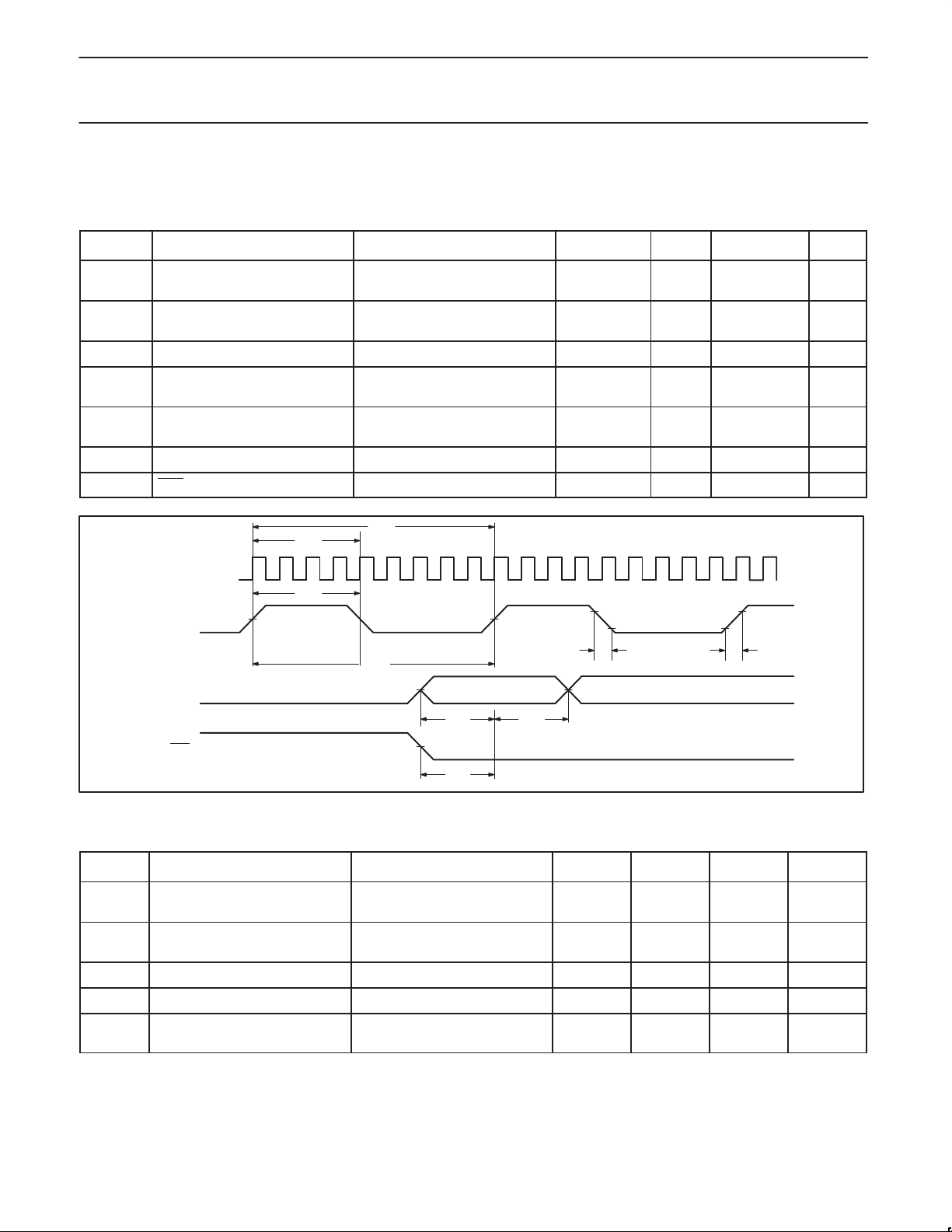
Philips Semiconductors Product specification
PRML Read Channel with PR4,
8/9 ENDEC, 4-Burst Servo
Data Separator Characteristics
Unless otherwise specified, recommended operating conditions apply.
Read Mode – Byte-Wide (Refer to Figure 23)
SYMBOL
t
RRC
t
FRC
t
RD
t
DC1
t
DC2
t
NS, tNH
t
SBS
Read clock rise time 0.8V to 2.4V
Read clock fall time 2.4V to 0.8V
RCLK pulse width Except during re-sync 4/9t
RCLK re-sync period
at SFC and RG falling edge
RCLK re-sync period
at code boundary detect
NRZx out set-up and hold time 20 ns
SBD set-up time 20 ns
VCO CLK
RCLK
PARAMETER TEST CONDITIONS MIN. NOM. MAX. UNIT
≤ 15 pF
C
L
≤ 15 pF
C
L
Measured from rising edge
to rising edge of RCLK
Measured from rising edge
to rising edge of RCLK
9 t
4 t
C
t
RD
C
P32P4910B
4 ns
3 ns
–5 4/9t
ORC
t
ORC
t
ORC
1.5V1.5V
2.4V
0.8V
0.8V
+5 ns
ORC
t
+2TC ns
ORC
2t
ORC
2.4V
ns
NRZ7–0
NRZP
SBD
Write Mode – Byte-Wide (Refer to Figure 24)
SYMBOL
t
RWC
t
FWC
t
SNRZ
t
HNRZ
t
PERR
Write clock rise time 0.8 to 2.0 V
Write clock fall time 2.0 to 0.8 V
NRZx set-up time 7 ns
NRZx hold time 3 ns
Measured from the rising edge of
WCLK to the transition of PERR
PARAMETER TEST CONDITIONS MIN. NOM. MAX. UNIT
t
ORC
1.5V (SB2) 1.5V (DT0)
t
NH
1.5V
t
t
NS
SBS
Figure 23. Byte-Wide Read Timing
≤ 15 pF
C
L
≤ 15 pF
C
L
t
FRC
t
RRC
4 ns
3 ns
41 ns
SM00169
1997 JuL 15
55
Page 56
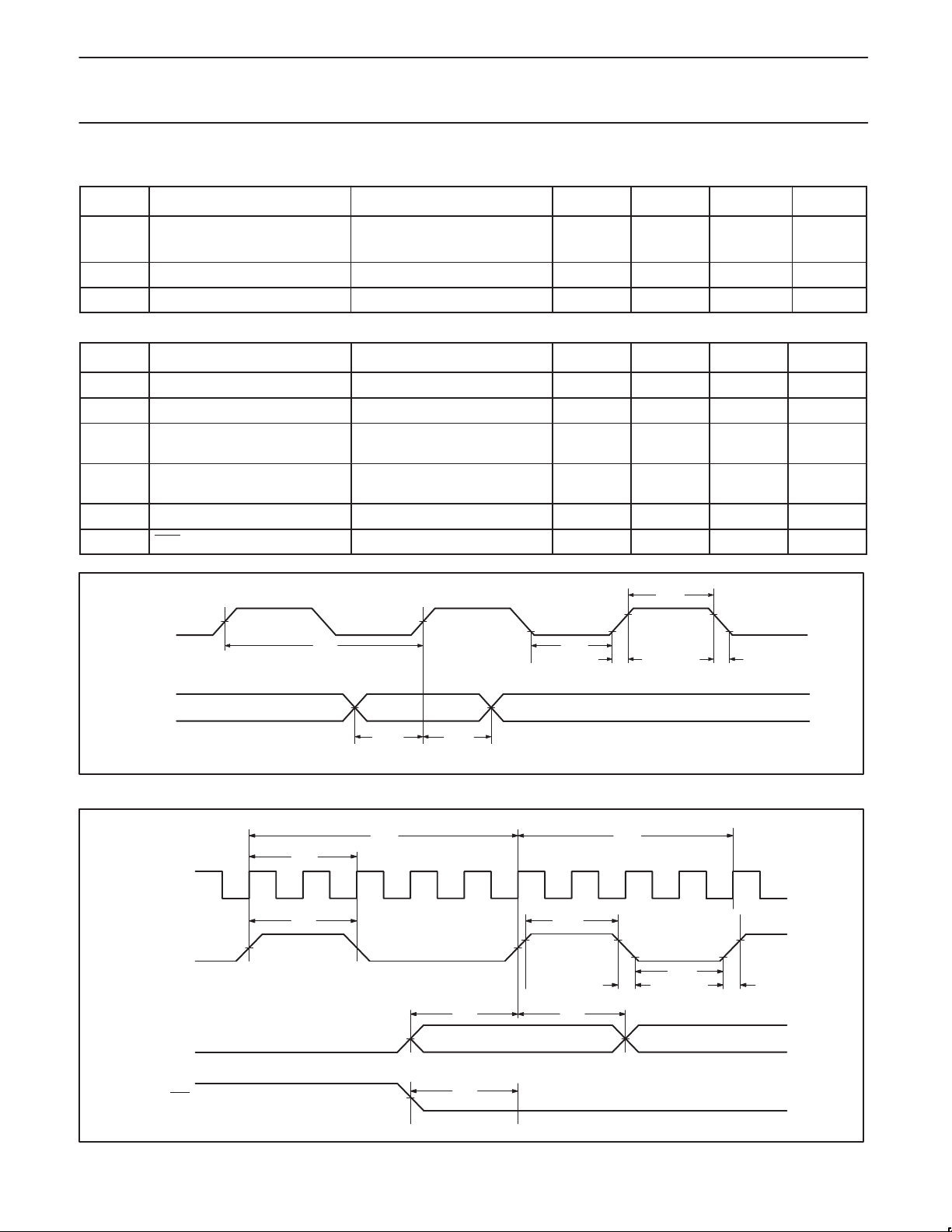
Philips Semiconductors Product specification
PRML Read Channel with PR4,
8/9 ENDEC, 4-Burst Servo
Write Data Output
SYMBOL
t
WD
t
RWD
t
FWD
Write data output position
accuracy
Write data output rise time 20% to 80% points 4 ns
Write data output fall time 80% to 20% points 4 ns
Read Mode – Nibble (Refer to Figure 25)
SYMBOL
t
RCL
t
RCH
t
RRC
t
FRC
tNS, t
t
SDL
RCLK Low time C
RCLK High time C
Read clock rise time 0.8V to 2.4V
Read clock fall time 2.4V to 0.8V
NRZx out set-up and hold time 5.6 ns
NH
SBD fall to RCLK Rising 7.5 ns
PARAMETER TEST CONDITIONS MIN. NOM. MAX. UNIT
Write precomp = 0,
C
PARAMETER TEST CONDITIONS MIN. NOM. MAX. UNIT
C
C
P32P4910B
T
–0.5 T
15 pF, T
L <
≤ 15 pF 2 * TC–3 2 * TC+3 ns
L
≤ 15 pF 2 * TC–3 2 * TC+3 ns
L
≤ 15 pF
L
≤ 15 pF
L
TBG
= 1/F
TBG
TBG
+0.5 ns
TBG
4 ns
3 ns
WCLK
NRZ7–0
NRZP
VCO CLK
RCLK
NRZ3–0
t
WCH
RWC
t
WC
1.5V 1.5V
t
SNRZ
2.0V
1.5V1.5V
t
HNRZ
0.8V
t
0.8V
WCL
t
Figure 24. Write Mode NRZ Interface Timing (byte-wide and nibble modes)
1.5V
5 t
C
2 t
C
1.5V
2.4V
t
RCH
t
NH
t
RD
t
NS
1.5V 1.5V
SB2(7:4) SB2(3:0)
t
4 t
FRC
C
2.4V
0.8V
t
RCL
0.8V
t
FWC
2.4V
2.0V
t
RRC
0.8V
SM00170
1997 JuL 15
SBD
t
SDL
1.5V
Figure 25. Nibble Read Timing
56
SM00006
Page 57
Philips Semiconductors Product specification
PRML Read Channel with PR4,
8/9 ENDEC, 4-Burst Servo
Write Mode – Nibble
SYMBOL
t
WC
t
WCL
t
WCH
t
RWC
t
FWC
t
SNRZ
t
HNRZ
WCLK period C
WCLK Low time C
WCLK High time C
Write clock rise time 0.8 to 2.0 V
Write clock fall time 2.0 to 0.8 V
NRZx set-up time 7 ns
NRZx hold time 3 ns
Write Precompensation
SYMBOL
TPC Write precomp time shift as a
percentage of T
PARAMETER TEST CONDITIONS MIN. NOM. MAX. UNIT
C
C
PARAMETER TEST CONDITIONS MIN. NOM. MAX. UNIT
TPC = 2.26 * WPC
TBG
0 ≤ WPC ≤ 15
P32P4910B
≤ 15 pF 24 ns
L
≤ 15 pF 5 ns
L
≤ 15 pF 5 ns
L
≤ 15 pF
L
≤ 15 pF
L
0.8 * TPC 1.2 * TPC %
4 ns
3 ns
Data Synchronizer PLL
SYMBOL
PARAMETER TEST CONDITIONS MIN. NOM. MAX. UNIT
FVCO VCO center frequency
VCO dynamic range in each
direction
VCO control gain and M,
M * KVCO
Charge Pump
Transconductance
KDI Idle Mode Phase
Detector Gain
Gm * M * KVCO
product accuracy
A * KVCO product accuracy A= 0.8 * (DRC/127) –30 +30 %
FLTR2+ – FLTR2– = 0V
0.8 * FVCO 1.2 * FVCO ns
FVCO = [(1.143 * DR) + 4.986] MHz
RR = 10.0 kΩ
FVCO = [(0.948 * DR) + 1.831] MHz
RR = 12.1 kΩ
–2.0V ≤ FLTR2+ – FLTR2– ≤ +2.0V ±25 %
ωi =2π/FVCO
0.11 * ωi * M 0.29 * ωι * M rad/(V*s)
M = 4.32 * (DR/127)
RR = 10.0 kΩ
M = 3.60 * (DR/127)
RR = 12.1 kΩ
–0.25V ≤ FLTR2+ – FLTR2– ≤ +0.25V
Gm = 350 µA/V
0.6 * Gm 1.4 * Gm A/V
during synchronization
KDI = 0.15 Gm * M
KDI µA/rad
RR = 10.0 kΩ
KDI = 0.18 Gm * M
RR = 12.1 kΩ
–28 +28 %
1997 JuL 15
57
Page 58
Philips Semiconductors Product specification
PRML Read Channel with PR4,
8/9 ENDEC, 4-Burst Servo
Servo Characteristics
Unless otherwise specified input is 15 MHz sine wave into DP/DN inputs, TPC/D1–0 = 01.
SMS = 0. STROBE and RESET
SYMBOL PARAMETER TEST CONDITIONS MIN. NOM. MAX. UNIT
MAXREF output voltage I
MAXREF load regulation I
BURST A, BURST B, BURST C,
BURST D output resistance
BURST A, BURST B, BURST C,
BURST D output low voltage
BURST A, BURST B, BURST C,
BURST D output swing
BURST A, BURST B, BURST C,
BURST D gain
Hold droop STROBE = Low
Channel to channel mismatch DP–DN = 1.4 Vpp 120 mV
Burst acquisition time to 95%
from reset time
durations are 1.0 µs and SBCC = 10.
= 0 mA 3.06 3.28 3.48 V
SOURCE
≤ 1.5 mA 40 mV
SOURCE
I
/ I
SOURCE
I
= 0.1 mA
SINK
RESET
DP/DN = 1.4 Vpp 2.59 2.8 3.01 V
0.3≤DP–DN≤1.4 1.85 2.0 2.15 V/Vppd
0V≤DP–DN≤0.3V 0 2.15 V/Vppd
RESET
DP–DN = 1.4 Vpp 0.5 µs
= 0.1 mA 50 Ω
SINK
= Low
= High
140 270 450 mV
P32P4910B
0.5 mV/µs
Burst reset to 5% DP–DN = 1.4 Vpp
Reset to strobe delay From rising RESET to rising
Minimum time between STROBE
pulses
RESET
STROBE
= Low
0.5 µs
20 ns
20 ns
1997 JuL 15
58
Page 59

Philips Semiconductors Product specification
PRML Read Channel with PR4,
8/9 ENDEC, 4–Burst Servo
DEFINITIONS
Data Sheet Identification Product Status Definition
Objective Specification
Preliminary Specification
Product Specification
Philips Semiconductors and Philips Electronics North America Corporation reserve the right to make changes, without notice, in the products,
including circuits, standard cells, and/or software, described or contained herein in order to improve design and/or performance. Philips
Semiconductors assumes no responsibility or liability for the use of any of these products, conveys no license or title under any patent, copyright,
or mask work right to these products, and makes no representations or warranties that these products are free from patent, copyright, or mask
work right infringement, unless otherwise specified. Applications that are described herein for any of these products are for illustrative purposes
only. Philips Semiconductors makes no representation or warranty that such applications will be suitable for the specified use without further testing
or modification.
Formative or in Design
Preproduction Product
Full Production
This data sheet contains the design target or goal specifications for product development. Specifications
may change in any manner without notice.
This data sheet contains preliminary data, and supplementary data will be published at a later date. Philips
Semiconductors reserves the right to make changes at any time without notice in order to improve design
and supply the best possible product.
This data sheet contains Final Specifications. Philips Semiconductors reserves the right to make changes
at any time without notice, in order to improve design and supply the best possible product.
P32P4910B
LIFE SUPPORT APPLICA TIONS
Philips Semiconductors and Philips Electronics North America Corporation Products are not designed for use in life support appliances, devices,
or systems where malfunction of a Philips Semiconductors and Philips Electronics North America Corporation Product can reasonably be expected
to result in a personal injury. Philips Semiconductors and Philips Electronics North America Corporation customers using or selling Philips
Semiconductors and Philips Electronics North America Corporation Products for use in such applications do so at their own risk and agree to fully
indemnify Philips Semiconductors and Philips Electronics North America Corporation for any damages resulting from such improper use or sale.
Philips Semiconductors
811 East Arques Avenue
P.O. Box 3409
Sunnyvale, California 94088–3409
Telephone 800-234-7381
Philips Semiconductors and Philips Electronics North America Corporation
register eligible circuits under the Semiconductor Chip Protection Act.
Copyright Philips Electronics North America Corporation 1996
All rights reserved. Printed in U.S.A.
 Loading...