

Page 1
Freescale Semiconductor
Technical Data
Single Gauge Driver
Document Number: MC33977
Rev. 2.0, 1/2007
The 33977 is a Serial Peripheral Interface (SPI) Controlled, stepper
motor gauge driver Integrated Circuit (IC). This monolithic IC consists
of a dual H-Bridge coil driver and its associated control logic. The HBridge drivers are used to automatically control the speed, direction,
and magnitude of current through the coils of a two-phase
instrumentation stepper motor, similar to an MMT-licensed AFIC 6405
of Switec MS-X156.xxx motor.
The 33977 is ideal for use in instrumentation systems requiring
distributed and flexible stepper motor gauge driving. The device also
eases the transition to stepper motors from air core motors by
emulating the damped air core pointer movement.
Features
• MMT-Licensed Two-Phase Stepper Motor Compatible
• Switec MS-X15.xxx Stepper Motor Compatible
• Minimal Processor Overhead Required
• Fully Integrated Pointer Movement and Position State Machine
with Air Core Movement Emulation
• 4096 Possible Steady State Pointer Positions
• 340° Maximum Pointer Sweep
• Maximum Acceleration of 4500°/s
2
• Maximum Pointer Velocity of 400°/s
• Analog Microstepping (12 Steps/Degrees of Pointer Movement)
• Pointer Calibration and Return to Zero (RTZ)
• Controlled via 16-Bit SPI Messages
• Internal Clock Capable of Calibration
• Low Sleep Mode Current
• Pb-Free Packaging Designated by suffix code EG
SINGLE GAUGE DRIVER
ORDERING INFORMATION
Device
MC33977DW/R2
MCZ33977EG/R2
33977
DW SUFFIX
EG SUFFIX (Pb-FREE)
98ASB42344B
24-PIN SOICW
Temperature
Range (T
- 40°C to 125°C 24 SOICW
)
A
Package
V
PWR
33977
V
5.0 V
DD
Regulator
MCU
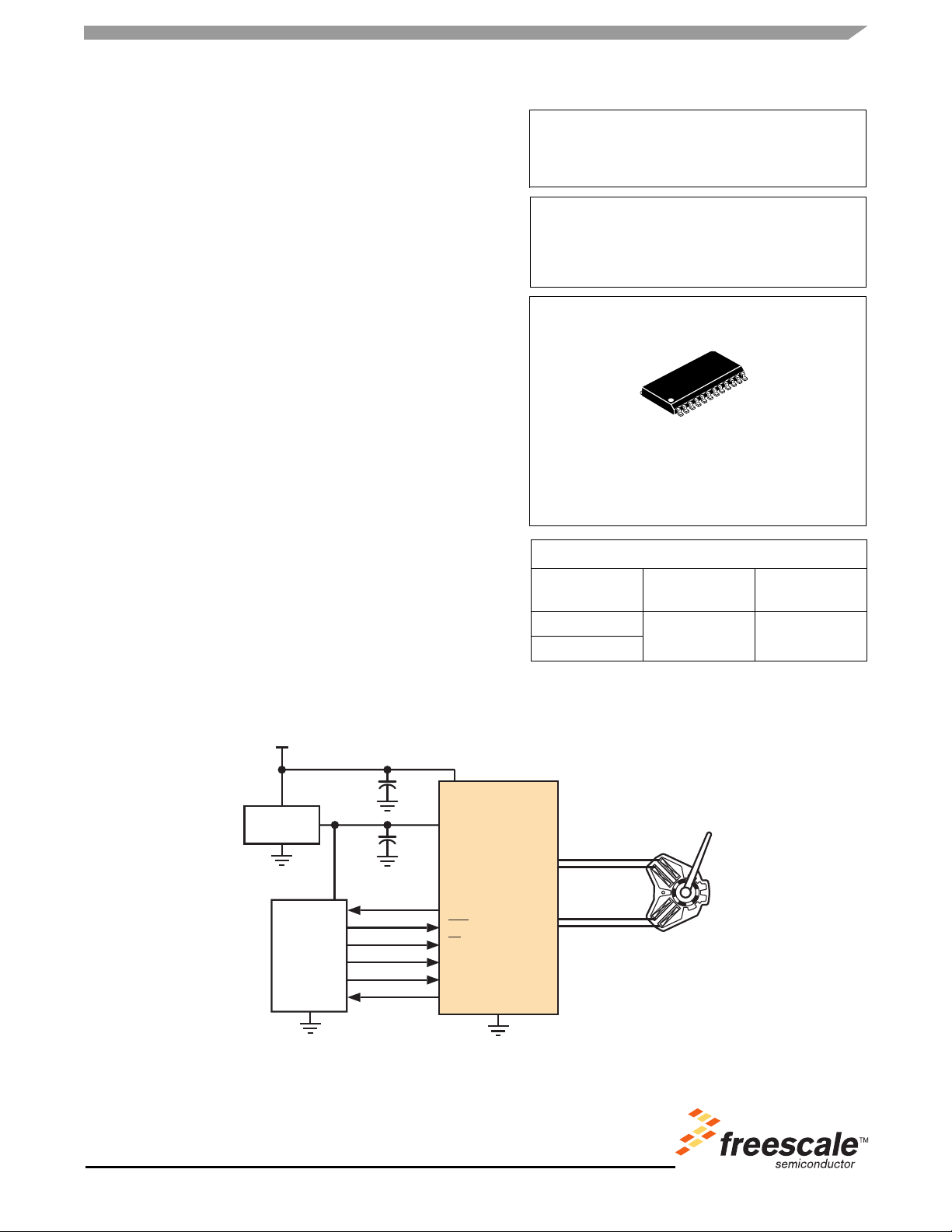
Figure 1. 33977 Simplified Application Diagram
Freescale Semiconductor, Inc. reserves the right to change the detail specifications,
as may be required, to permit improvements in the design of its products.
© Freescale Semiconductor, Inc., 2007. All rights reserved.
VPWR
VDD
RTZ
RST
CS
SCLK
SI
SO
GND
SIN+
SIN-
COS+
COS-
Motor
Page 2
INTERNAL BLOCK DIAGRAM
INTERNAL BLOCK DIAGRAM
VPWR
VDD
CS
SCLK
SO
RST
INTERNAL
REGULATOR
COS
SPI
SI
LOGIC
UNDER
-
AND
OVERVOLTAGE
DETECT
STATE
MACHINE
ILIM
OVERTEMPERATURE
DETECT
SIGMA-DELTA
ADC
H-BRIDGE
AND
CONTROL
SIN
VDD
MULTIPLEXER
COS+
COS-
SIN+
SIN-
OSCILLATOR
AGND
GND (8)
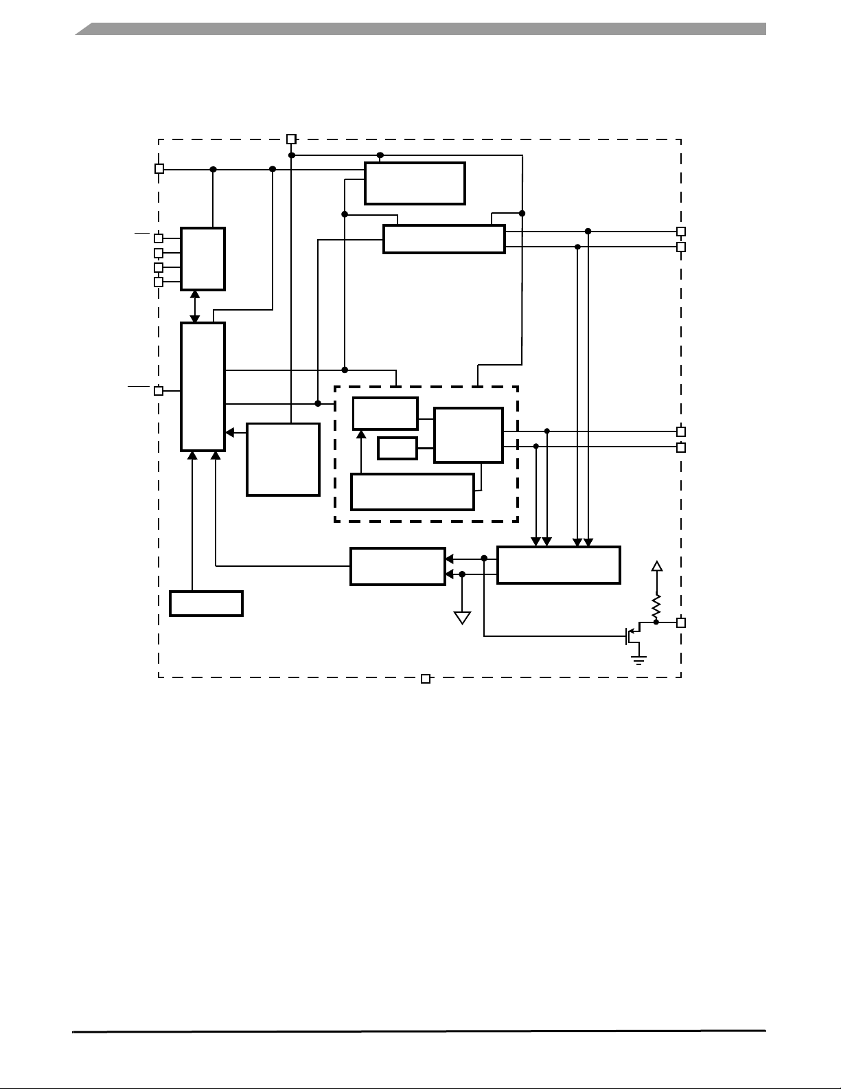
Figure 2. 33977 Simplified Internal Block Diagram
RTZ
33977
Analog Integrated Circuit Device Data
2 Freescale Semiconductor
Page 3
PIN CONNECTIONS
PIN CONNECTIONS
COS+
COS-
SIN+
SINGND
GND
GND
GND
CS
SCLK
SO
SI
NC
NC
NC
NC
GND
GND
GND
GND
VPWR
RST
VDD
RTZ
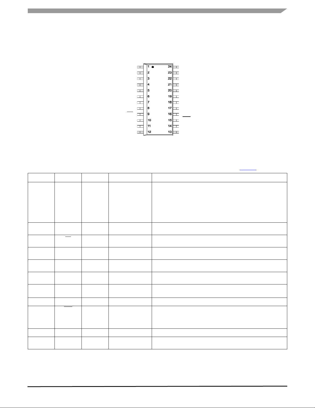
Figure 3. 33977 Pin Connections
Table 1. 33977 Pin Definitions
A functional description of each pin can be found in the Functional Pin Descri ption section beginning onpage 10.
Pin Pin Name Pin Function Formal Name Definition
1
2
3
4
5 to 8,
17 to 20
9
10 SCLK
11 SO
12
13 RTZ
14 VDD
15 RST
16 VPWR
21, 22, 23, 24
(MS Motor
Pin #)
COS+ (MS #4)
COS- (MS #3)
SIN+ (MS #1)
SIN- (MS #2)
GND
CS
SI
NC
Output
N/A
Input
Input
Output
Input
Multiplexed
Output
Input
Input
Input
–
H-Bridge Outputs 0 Each pin is the output of a half-bridge, designed to source or sink current.
Ground Ground pins
Chip Select This pin is connected to a chip select output of a Large Scale Integration
(LSI) Master IC and controls which device is addressed.
Serial Clock This pin is connected to the SCLK pin of the master device and acts as a
bit clock for the SPI port.
Serial Output This pin is connected to the SPI Serial Data Input pin of the Master device
or to the SI pin of the next device in a daisy chain.
Serial Input This pin is connected to the SPI Serial Data Output pin of the Master
device from which it receives output command data.
Return to Zero This is a multiplexed output pin for the non-driven coil, during a Return to
Zero (RTZ) event.
Voltage This SPI and logic power supply input will work with 5.0 V supplies.
Reset This pin is connected to the Master and is used to reset the device, or
place it into a sleep state by driving it to Logic [1]. When this pin is driven
to Logic [0], all internal logic is forced to the default state. This input has
an internal active pull-up.
Battery Voltage Power supply
No Connect These pins are not connected to any internal circuitry, or any other pin,
and may be connected to the board where convenient.
33977
Analog Integrated Circuit Device Data
Freescale Semiconductor 3
Page 4

ELECTRICAL CHARACTERISTICS
MAXIMUM RATINGS
ELECTRICAL CHARACTERISTICS
MAXIMUM RATINGS
Table 2. Maximum Ratings
All voltages are with respect to ground unless otherwise noted. Exceeding these ratings may cause a malfunction or
permanent damage to the device.
Ratings Symbol Value Unit
ELECTRICAL RATINGS
Power Supply Voltage
Steady-State
Input Pin Voltage
SIN± COSI± Continuous Current Per Output
ESD Voltage
(1)
(2)
(3)
Human Body Model (HBM)
Machine Model (MM)
Charge Device Model (CDM)
THERMAL RATINGS
Operating Temperature
Ambient
Junction
Storage Temperature T
Thermal Resistance
Junction-to-Ambient
Junction-to-Lead
Peak Package Reflow Temperature During Reflow
(4), (5)
Notes
1. Exceeding voltage limits on Input pins may cause permanent damage to the device.
2. Output continuous output rating so long as maximum junction temperature is not exceeded. Operation at 125°C ambient temperature
will require maximum output current computation using package thermal resistances.
3. ESD testing is performed in accordance with the Human Body Model (HBM) (C
(C
ZAP
= 200 pF, R
= 0 Ω), and the Charge Device Model (CDM).
ZAP
4. Pin soldering temperature limit is for 10 seconds maximum duration. Not designed for immersion soldering. Exceeding these limits may
cause malfunction or permanent damage to the device.
5. Freescale’s Package Reflow capability meets Pb-free requirements for JEDEC standard J-STD-020C. For Peak Package Reflow
Temperature and Moisture Sensitivity Levels (MSL),
Go to www.freescale.com, search by part number [e.g. remove prefixes/suffixes and enter the core ID to view all orderable parts. (i.e.
MC33xxxD enter 33xxx), and review parametrics.
V
PWRSS
V
IN
I
OUTMAX
V
ESD
T
A
T
J
STG
R
ΘJA
R
ΘJL
T
PPRT
= 100 pF, R
ZAP
-0.3 to 41
-0.3 to 7.0 V
40 mA
±2000
±2000
±200
-40 to 125
-40 to 150
-55 to 150 °C
°C/W
60
20
Note 5
= 1500 Ω), the Machine Model (MM)
ZAP
V
V
°C
°C
33977
Analog Integrated Circuit Device Data
4 Freescale Semiconductor
Page 5

STATIC ELECTRICAL CHARACTERISTICS
ELECTRICAL CHARACTERISTICS
STATIC ELECTRICAL CHARACTERISTICS
Table 3. Static Electrical Characteristics
Characteristics noted under conditions 4.75 V < VDD < 5.25 V, and - 40°C < TA< 125°C, unless otherwise noted. Typical
values noted reflect the approximate parameter means at T
Characteristic Symbol Min Typ Max Unit
POWER INPUT (VDD)
Battery Supply Voltage Range
Fully Operational
Limited Operation
V
Supply Current
PWR
Gauge Outputs ON, No Output Loads
VPWR Supply Current (All Outputs Disabled)
Reset = Logic [0], V
Reset = Logic [0], V
Overvoltage Detection Level
Undervoltage Detection Level
Logic Supply Voltage Range (5.0 V Nominal Supply)
Under VDD Logic Reset
VDD Supply Current
Sleep: Reset Logic [0]
Outputs Enabled
POWER OUTPUT (SIN-, SIN+, COS-, COS+)
Microstep Output (Measured Across Coil Outputs)
SIN± (COS±) (Refer to Pin Definitions onpage 3)
R
= 200 Ω, PE6 = 0
OUT
Steps Pin Definitions
6, 18, 0, 12
5, 7, 17, 19 1, 11, 13, 23
4, 8, 16, 20 2, 10, 14, 22
3, 9, 15, 21 3, 9, 15, 21
2, 10, 14, 22 5, 7, 17, 19
1, 11, 13, 23 5, 7, 17, 19
0, 12 6, 18
Full Step Active Output (Measured Across Coil Outputs)
SIN± (COS±), Steps 1,3 (Pin Definitions 0 and 2)
Notes
6. Outputs and logic remain active; however, the larger coil voltage levels may be clipped. The reduction in drive voltage may result in a
loss of position control.
7. The logic will reset at some level below the specified Limited Operational minimum.
8. Outputs will disable and must be re-enabled via the PECCR command.
9. Outputs remain active; however, the reduction in drive voltage may result in a loss of position control.
10. See Figure 7.
(6), (7)
DD
DD
= 5.0 V
= 0 V
(8)
(9)
(10)
= 25°C under nominal conditions unless otherwise noted.
A
V
PWR
I
PWR
6.5
4.0
– 26
26
– 4.0 6.0
I
PWRSLP1
I
PWRSLP2
V
PWROV
V
PWRUV
V
DD
V
DDUV
I
DDOFF
I
DDON
V
ST6
V
ST5
V
ST4
V
ST3
V
ST2
V
ST1
V
ST0
V
FS
–
–
42
15
60
25
26 32 38 V
5.0 5.6 6.2 V
4.5 5.0 5.5 V
– – 4.5 V
4.82
0.94 V
0.84 V
0.68 V
0.47 V
0.23 V
0.1
–
–
ST6
ST6
ST6
ST6
ST6
40
1.0
5.3
0.97 V
0.87 V
0.71 V
0.50 V
0.26 V
0.0
ST6
ST6
ST6
ST6
ST6
65
1.8
6.0
1.0 V
0.96 V
0.8 V
0.57 V
0.31 V
0.1
ST6
ST6
ST6
ST6
ST6
4.9 5.3 6.0
V
mA
µA
µV
mA
V
V
33977
Analog Integrated Circuit Device Data
Freescale Semiconductor 5
Page 6
ELECTRICAL CHARACTERISTICS
STATIC ELECTRICAL CHARACTERISTICS
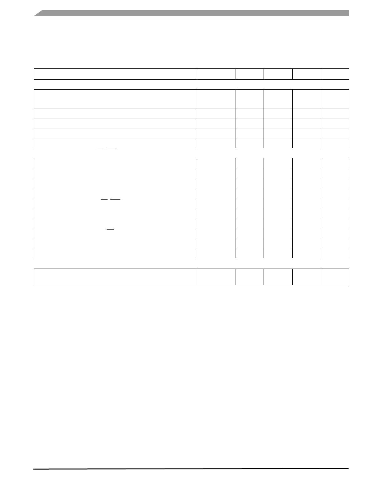
Table 3. Static Electrical Characteristics (continued)
Characteristics noted under conditions 4.75 V < VDD < 5.25 V, and - 40°C < TA< 125°C, unless otherwise noted. Typical
values noted reflect the approximate parameter means at TA = 25°C under nominal conditions unless otherwise noted.
Characteristic Symbol Min Typ Max Unit
POWER OUTPUT (SIN-, SIN+, COS-, COS+) (Continued)
Microstep Full Step Output (Measured from Coil Low Side to Ground)
SIN± (COS±) I
Output Flyback Clamp
Output Current Limit (Output - V
Overtemperature Shutdown
Overtemperature Hysteresis
OUT
= 30 mA
(11)
(12)
(12)
ST6
)
CONTROL I/O (SI, SCLK, CS, RST, SO)
Input Logic High Voltage
Input Logic Low Voltage
Input Logic Voltage Hysteresis
(12)
(12)
(12)
Input Logic Pull-Down Current (SI, SCLK)
Input Logic Pull-Up Current (CS, RST)
SO High State Output Voltage (IOH = 1.0 mA)
SO Low State Output Voltage (IOL = 1.6 mA)
SO Tri-State Leakage Current (CS = 3.5 V)
Input Capacitance
SO Tri-State Capacitance
(13)
(13)
ANALOG TO DIGITAL CONVERTER (RTZ ACCUMULATOR COUNT)
ADC Gain
(12), (14)
Notes
11. Outputs remain active; however, the reduction in drive voltage may result in a loss of position control.
12. This parameter is guaranteed by design; however, it is not production tested.
13. Capacitance not measured. This parameter is guaranteed by design; however, it is not production tested.
14. Reference RTZ Accumulator (Typical) on page 30
V
V
I
LIM
T
T
HYST
V
V
V
INHYST
I
DWN
I
V
SOH
V
I
SOLK
C
C
G
ADC
LS
FB
SD
IH
IL
UP
SOL
IN
SO
0.0 0.1 0.3
– V
ST6
+ 0.5 V
+ 1.0 V
ST6
40 100 170 mA
155 – 180 °C
8.0 – 16 °C
2.0 – – V
– – 0.8 V
– 100 – mV
3.0 – 20 µA
5.0 – 20 µA
0.8 V
DD
– – V
– 0.2 0.4 V
-5.0 0.0 5.0 µA
– 4.0 12 pF
– – 20 pF
100 188 270 Counts/V/
V
ms
33977
Analog Integrated Circuit Device Data
6 Freescale Semiconductor
Page 7

DYNAMIC ELECTRICAL CHARACTERISTICS
ELECTRICAL CHARACTERISTICS
DYNAMIC ELECTRICAL CHARACTERISTICS
Table 4. Dynamic Electrical Characteristics
Characteristics noted under conditions 4.75 V < VDD < 5.25 V, and - 40°C < TA < 125°C, unless otherwise noted. Typical
values noted reflect the approximate parameter means at T
Characteristic Symbol Min Typ Max Unit
POWER OUTPUT AND CLOCK TIMINGS (SIN+, SIN-, COS+, COS-) CS
SIN± (COS±) Output Turn ON Delay Time (Time from Rising CS
Enabling Outputs to Steady State Coil Voltages and Currents)
SIN± (COS±) Output Turn OFF Delay Time (Time from Rising CS
Disables Outputs to Steady State Coil Voltages and Currents)
Uncalibrated Oscillator Cycle Time
Calibrated Oscillator Cycle Time
Calibration Pulse = 8.0 µs, PECCR D4 = Logic [0]
Calibration Pulse = 8.0 µs, PECCR D4 = Logic [1]
Maximum Pointer Speed
Maximum Pointer Acceleration
SPI INTERFACE TIMING (CS, SCLK, SO, SI, RST)
Recommended Frequency of SPI Operation
Falling Edge of CS to Rising Edge of SCLK (Required Setup Time)
Falling Edge of SCLK to Rising Edge of CS (Required Setup Time)
SI to Falling Edge of SCLK (Required Setup Time)
Falling Edge of SCLK to SI (Required Hold Time)
SO Rise Time
CL = 200 pF
SO Fall Time
CL = 200 pF
SI, CS, SCLK, Incoming Signal Rise Time
SI, CS, SCLK, Incoming Signal Fall Time
Falling Edge of RST to Rising Edge of RST (Required Setup Time)
Rising Edge of CS to Falling Edge of CS (Required Setup Time)
Falling Edge of RST to Rising Edge of CS (Required Setup Time)
Notes
15. Maximum specified time for the 33977 is the minimum guaranteed time needed from the microcontroller.
16. The minimum and maximum value will vary proportionally to the internal clock tolerance. These numbers are based on an ideally
calibrated clock frequency of 1.0 MHz. These are not 100 percent tested.
17. The 33977 shall meet all SPI interface timing requirements specified in the SPI Interface Timing section of this table, over the specified
temperature range. Digital interface timing is based on a symmetrical 50 percent duty cycle SCLK Clock Period of 33 ns. The device shall
be fully functional for slower clock speeds. Reference
18. The required setup times specified for the 33977 are the minimum time needed from the microcontroller to guarantee correct operation.
19. Rise and Fall time of incoming SI, CS, and SCLK signals suggested for design consideration to prevent the occurrence of double pulsing.
20. The value is for a 1.0 MHz calibrated internal clock. The value will change proportionally as the internal clock frequency changes.
(16)
(16)
(17)
(18)
(18)
(19)
(19)
= 25°C under nominal conditions unless otherwise noted.
A
t
(15)
(15)
(18)
(18)
DLYON
t
DLYOFF
t
CLU
t
CLC
V
MAX
A
MAX
f
SPI
t
LEAD
t
LAG
t
SISU
t
SIHOLD
t
RSO
– – 1.0
– – 1.0
0.65 1.0 1.7 µs
1.0
0.9
1.1
1.0
– – 400 °/s
– – 4500 °/s
– 1.0 2.0 MHz
167 – – ns
167 – – ns
– 25 83 ns
– 25 83 ns
– 25 50
t
FSO
– 25 50
(18)
(18), (20)
(18)
t
RSI
t
FIS
t
RST
W
t
CS
t
EN
– – 50 ns
– – 50 ns
– – 3.0 µs
– – 5.0 µs
– – 5.0 µs
Figure 4 and 5.
ms
ms
µs
1.2
1.1
ns
ns
2
33977
Analog Integrated Circuit Device Data
Freescale Semiconductor 7
Page 8

ELECTRICAL CHARACTERISTICS
DYNAMIC ELECTRICAL CHARACTERISTICS
Table 4. Dynamic Electrical Characteristics (continued)
Characteristics noted under conditions 4.75 V < VDD < 5.25 V, and - 40°C < TA < 125°C, unless otherwise noted. Typical
values noted reflect the approximate parameter means at TA = 25°C under nominal conditions unless otherwise noted.
Characteristic Symbol Min Typ Max Unit
SPI INTERFACE TIMING (CS, SCLK, SO, SI, RST) ‘ (CONTINUED)
(24)
(22)
(23)
t
SOEN
t
SODIS
t
VALID
– – 145 ns
– 1.3 4.0 µs
ns
– 90 150
Time from Falling Edge of CS to SO Low Impedance
Time from Falling Edge of CS to SO High Impedance
Time from Rising Edge of SCLK to SO Data Valid
0.2 VDD = SO = 0.8 VDD, CL = 200 pF
Notes
21. The 33977 shall meet all SPI interface timing requirements specified in the SPI Interface Timing section of this table, over the specified
temperature range. Digital interface timing is based on a symmetrical 50 percent duty cycle SCLK Clock Period of 33 ns. The device shall
be fully functional for slower clock speeds.
22. Time required for output status data to be terminated at SO 1.0 kΩ load on SO.
23. Time required for output status data to be available for use at SO 1.0 kΩ load on SO.
24. Time required to obtain valid data out from SO following the rise of SCLK.
33977
Analog Integrated Circuit Device Data
8 Freescale Semiconductor
Page 9
RST
t
WRST
0.2 V
DD
TIMING DIAGRAMS
ELECTRICAL CHARACTERISTICS
TIMING DIAGRAMS
t
CS
V
IN
V
IL
CS
SCLK
SI
0.7 V
DD
SCLK
SO
Low-to-High
SO
High-to-Low
0.7 V
0.2 V
0.2 V
t
LEAD
DD
DD
0.7 V
DD
DD
t
SISU
Valid Don’t Care Valid Don’t CareDon’t Care
t
SI(HOLD)
t
RSI
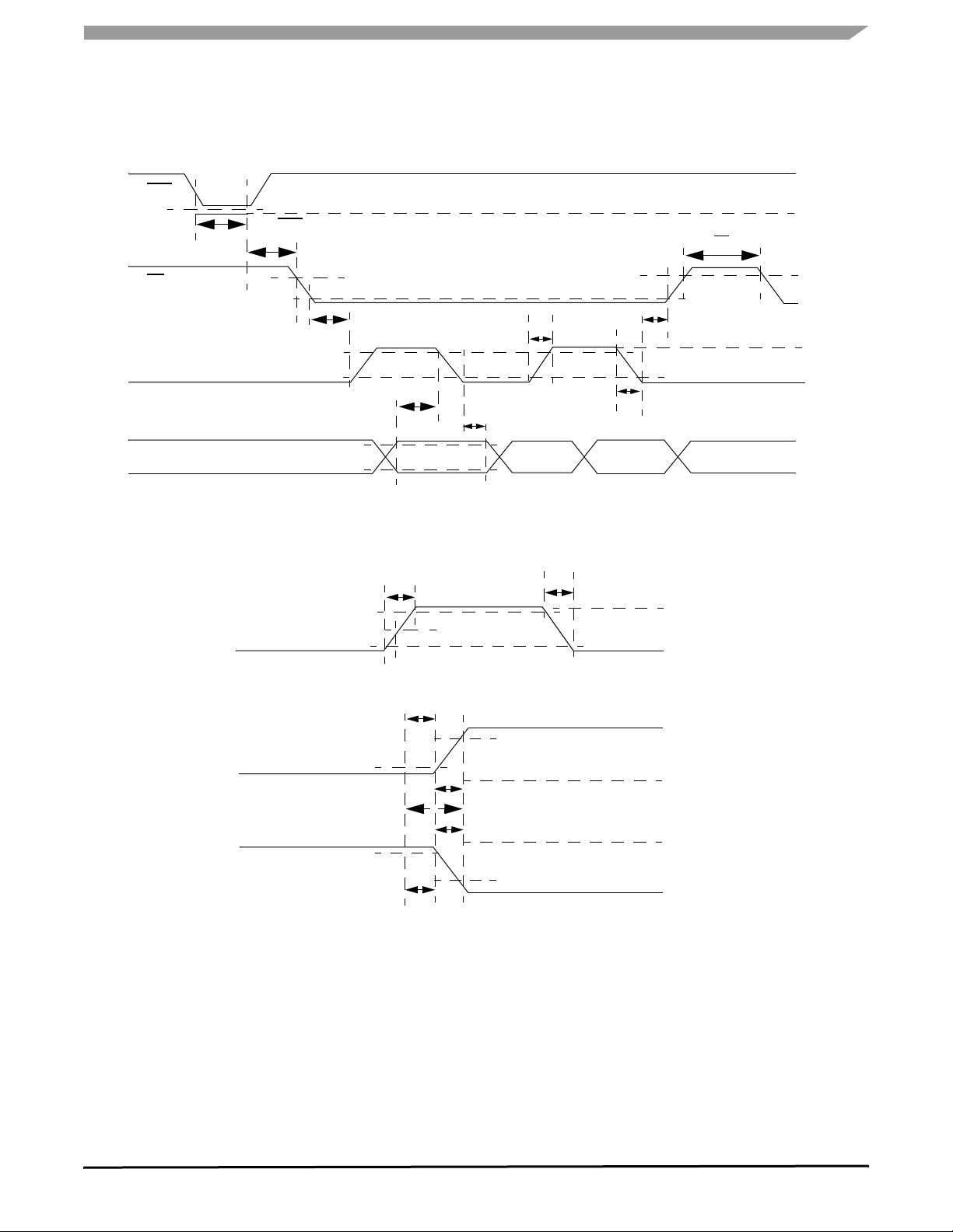
Figure 4. Input Timing Switching Characteristics
t
FIS
3.5V
0.2 VDD
V
DD
0.7
t
SO(DIS)
t
SO(EN)
t
VALID
t
RSI
50%
t
RSO
t
RSO
0.7 VDD
0.2 VDD
0.7 V
1.0V
DD
t
FIS
V
IH
V
IL
t
LAG
V
OH
V
OL
V
OH
V
OL
V
OH
V
OL
V
IH
Figure 5. Valid Data Delay Time and Valid Time Waveforms
33977
Analog Integrated Circuit Device Data
Freescale Semiconductor 9
Page 10

FUNCTIONAL DESCRIPTION
FUNCTIONAL PIN DESCRIPTION
FUNCTIONAL DESCRIPTION
INTRODUCTION
This 33977 is a single-packaged, Serial Peripheral
INterface (SPI) controlled, single stepper motor gauge driver
integrated circuit (IC). This monolithic stepper IC consists of
[deleted two per D. Mortensen] a dual output H-Bridge coil
driver [deleted plural s for accurate tense] and the
FUNCTIONAL PIN DESCRIPTION
COSINE POSITIVE (COS0+)
The H-Bridge pins linearly drive the sine and cosine coils
of a stepper motor, providing four-quadrant operation.
COSINE NEGATIVE (COS0-)
The H-Bridge pins linearly drive the sine and cosine coils
of a stepper motor, providing four-quadrant operation.
SINE POSITIVE (SIN+)
The H-Bridge pins linearly drive the sine and cosine coils
of a stepper motor, providing four-quadrant operation.
SINE NEGATIVE (SIN-)
The H-Bridge pins linearly drive the sine and cosine coils
of a stepper motor, providing four-quadrant operation.
GROUND (GND)
Ground pins.
CHIP SELECT (CS)
The pin enables communication with the master device.
When this pin is in a logic [0] state, the 33977 is capable of
transferring information to, and recei vi n g i nf ormation from,
the master. The 33977 latches data in from the Input Shift
registers to the addressed registers on the rising edge of
The output driver on the SO pin is enabled when CS is
logic [0]. When CS is logic high, signals at the SCLK and SI
pins are ignored and the SO pin is tri-stated (high
impedance).
to a logic [0] state when SCLK is logic [0].
pull-up (I
of the Static Electrical Characteristics Table.
CS will only be transitioned from a logic [1] state
CS has an internal
) connected to the pin, as specified in the section
UP
CS.
associated control logic. The dual H-Bridge driver is used to
automatically control the speed, direction, and magnitude of
current through the coils of a two-phase instrumentation
stepper motor, similar to an MMT-licensed AFIC 6405 of
Switec MS-X 156.xxx motor.
SCLK has an internal pull down (l
section of the Static Electrical Characteristics Table. When
CS is logic [1], signals at the SCLK and SI pins are ignored
and SO is tri-stated (high impedance). Refer to the data
transfer
Timing Diagrams on page 9.
), as specified in the
DWN
SERIAL OUTPUT (SO)
The SO data pin is a tri-stateable output from the Shift
register. The Status register bits are the first 16 bits shifted
out. Those bits are followed by the message bits clocked in
FIFO, when the device is in a daisy chain connection or being
sent words that are multiples of 16 bits. Data is shifted on the
rising edge of the SCLK signal. The SO pin will remain in a
high impedance state until the
state.
CS pin is put into a logic low
SERIAL INPUT (SI)
The SI pin is the input of the SPI. Serial input information
is read on the falling edge of SCLK. A 16-bit stream of serial
data is required on the SI pin, beginning with the most
significant bit (MSB). Messages that are not multiples of 16
bits (e.g., daisy chained device messages) are ignored. After
transmitting a 16-bit word, the
(logic [1]) before transmitting a new word. SI information is
ignored when
CS is in a logic high state.
CS pin must be de-asserted
RETURN TO ZERO (RTZ)
This is a multiplexed output pin for the non-driven coil,
during a Return to Zero (RTZ) event.
VOLTAGE (VDD)
The SPI and logic power supply input will work with 5.0 V
supplies.
SERIAL CLOCK (SCLK)
SCLK clocks the Internal Shift registers of the 33977
device. The SI pin accepts data into the Input Shift register on
the falling edge of the SCLK signal, while the Serial Output
pin (SO) shifts data information out of the SO Line Driver on
the rising edge of the SCLK signal. It is important that the
SCLK pin be in a logic [0] state whenever the
transition.
33977
10 Freescale Semiconductor
CS makes any
RESET (RST)
If the master decides to reset the device, or place it into a
sleep state, the
the RST pin forces all internal logic to the known default state.
This input has an internal active pull-up.
RST pin is driven to a Logic [0]. A Logic [0] on
VOLTAGE POWER (VPWR)
This is the power supply pin.
Analog Integrated Circuit Device Data
Page 11

FUNCTIONAL INTERNAL BLOCK DESCRIPTION (OPTIONAL)
FUNCTIONAL INTERNAL BLOCK DESCRIPTION (OPTIONAL)
FUNCTIONAL DESCRIPTION
SPI Logic
Under and
Overvoltage
Detect
Figure 6. Functional Internal 33977 Block Illustration
SERIAL PERIPHERAL INTERFACE (SPI)
This circuitry manages incoming messages and outgoing
status data.
LOGIC
This design element includes internal logic including state
machines and message decoding.
INTERNAL REFERENCE
This design element is used for step value levels.
UNDER AND OVERVOLTAGE DETECTION
This design element detects when V
normal operating range.
is out of the
PWR
Internal
Reference
Oscillator
RTZ
H-Bridge
and Control
OSCILLATOR
The internal oscillator generates the internal clock for all
timing critical features.
H-BRIDGE AND CONTROL
This circuitry contains the output coil drivers and the
multiplexers necessary for four quadrant operation and RTZ
sequencing. This circuitry is repeated for the Sine and Cosine
coils.
• Overtemperature — Each output includes an
overtemperature sensing circuit
• ILIM — Each output is current limited
RETURN TO ZERO (RTZ)
This circuitry outputs the voltage present on the non-driven
coil during RTZ operation.
33977
Analog Integrated Circuit Device Data
Freescale Semiconductor 11
Page 12
FUNCTIONAL DEVICE OPERATION
OPERATIONAL MODES
FUNCTIONAL DEVICE OPERATION
OPERATIONAL MODES
STATE MACHINE OPERATION
The 33977 is ideal for use in instrumentation systems
requiring distributed and flexible stepper motor gauge driving.
The device also eases the transition to stepper motors from
air core motors by emulating the air core pointer movement
with little additional processor bandwidth utilization. The twophase stepper motor has maximum allowable velocities and
acceleration and deceleration. The purpose of the stepper
motor state machine is to drive the motor with the maximum
performance while remaining within the motor’s voltage,
velocity, and acceleration constraints.
A requirement of the state machine is to ensure the
deceleration phase begins at the correct time and pointer
position. When commanded, the motor [will deleted PV]
accelerates constantly to the maximum velocity, and then it
moves toward the commanded position at the maximum
velocity. Eventually, the pointer reaches the calculated
location where the movement has to decelerate, safely
slowing to a stop at the desired position. During the
deceleration phase, the motor does [will deleted PV] not
exceed the maximum deceleration.
During normal operation, both stepper motor rotors are
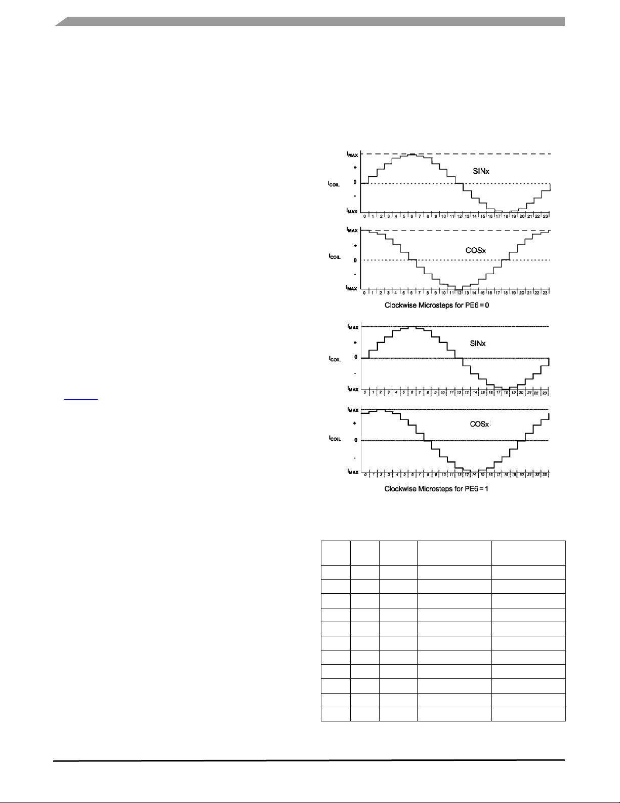
microstepped at 24 steps per electrical revolution, illustrated
in Figure 7. A complete electrical revolution results in two
degrees of pointer movement. There is a second smaller
[parentheses removed-unnecessary] state machine in the IC
controlling these microsteps. The smaller state machine
receives clockwise or counter-clockwise index commands at
timed intervals, thereby stepping the motor in the appropriate
direction by adjusting the current in each coil. Normalized
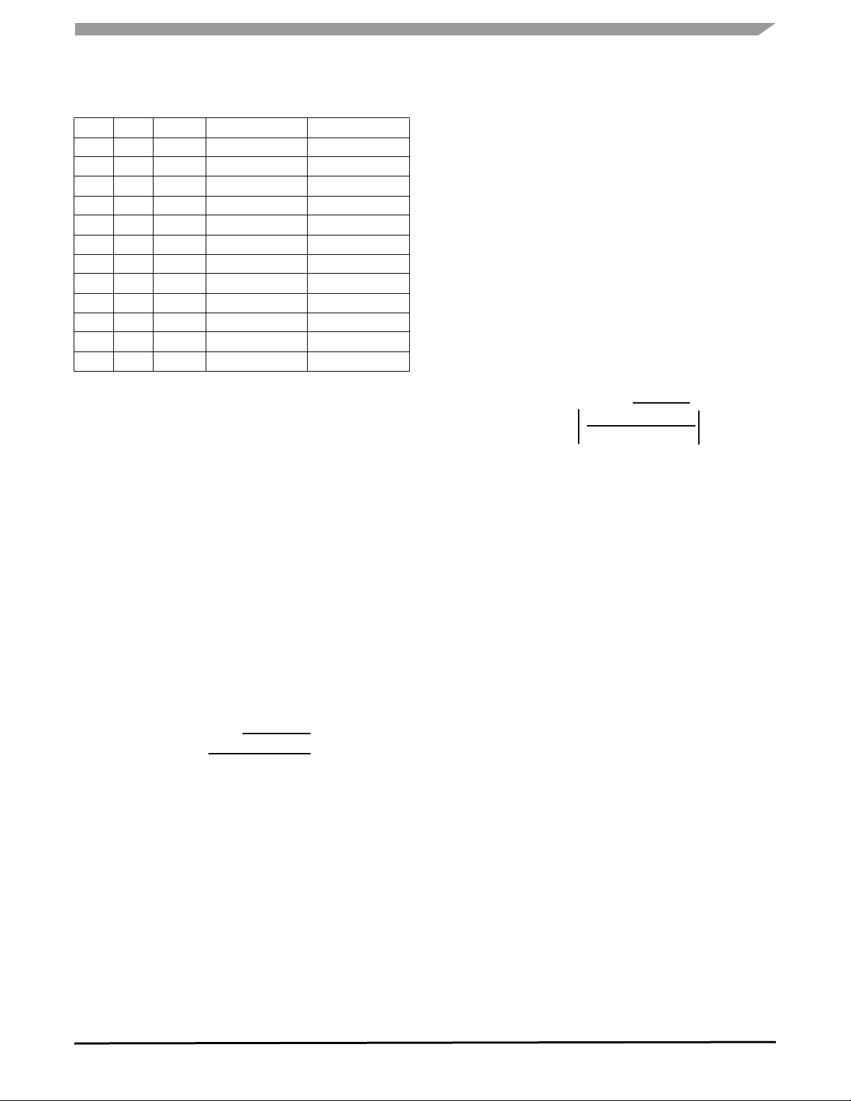
values are provided in
Table 5.
Figure 7. Clockwise Microsteps
Table 5. Coil Step Value
33977
Step
Angle
0
1
2
3
4
5
6
7
105 0.966 -0.259 0.259
8
120 0.866 -0.5 0.0
9
135 0.707 -0.707 -0.259
10
150 0.5 -0.866 -0.500
SINE
(Angle)*
0.0 0.0 1.0 0.866
15 0.259 0.965 0.966
30 0.5 0.866 1.0
45 0.707 0.707 0.966
60 0.866 0.5 0.866
75 0.966 0.259 0.707
90 1.0 0.0 0.500
COS (Angle -30)*
PE6=0
COS (Angle -30)*
PE6=1
Analog Integrated Circuit Device Data
12 Freescale Semiconductor
Page 13
FUNCTIONAL DEVICE OPERATION
2
0
OPERATIONAL MODES
Table 5. Coil Step Value
11
165 0.259 -0.966 -0.707
12
180 0.0 -1.0 -0.866
13
195 -0.259 -0.966 -0.966
14
210 -0.5 -0.867 -1.0
15
225 -0.707 -0.707 -0.966
16
240 -0.866 -0.5 -0.866
17
255 -0.966 -0.259 -0.707
18
270 -1.0 0.0 -0.500
19
285 -0.966 0.259 -0.259
20
300 -0.866 0.5 0.0
21
315 -0.707 0.707 0.259
22
330 -0.5 0.866 0.500
23
345 -0.259 0.966 0.707
* Denotes normalized values
The motor is stepped by providing index commands at
intervals. The time between steps defines the motor velocity
and the changing time defines the motor acceleration.
The state machine uses a table to define the allowed time
and the maximum velocity. A useful side effect of the table is
that it also allows the direct determination of the position at
which the velocity should reduce to stop the motor at the
desired position.
Motor motion equations follow: [reworded for efficient use
of space]
(The units of position are steps and velocity and
acceleration are in steps/second and steps/second
2
.)
From an initial position of 0 with an initial velocity (u), the
motor position (s) at a time (t) is:
s = ut + 1/2 at
For unit steps, the time between steps is:
⇒
t =
- u +
√ u
2
+ 2a
a
This defines the time increment between steps when the
motor is initially traveling at a velocity u. In the ROM, this time
is quantized to multiples of the system clock by rounding
upwards, ensuring acceleration never exceeds the allowed
value. The actual velocity and acceleration is calculated from
the time step actually used. Using:
v2 = u2 + 2as
and
v = u + at
and solving for v in terms of u, s, and t gives:
v = 2/t - u
The correct value of t to use in the equation is the
quantized value obtained above.
From these equations, a set of recursive equations can be
generated to give the allowed time step between motor
indexes when the motor is accelerating from a stop to its
maximum velocity.
Starting from a position p of 0 and a velocity v of 0, these
equations define the time interval between steps at each
position. To drive the motor at maximum performance, index
commands are given to the motor at these intervals. A table
is generated giving the time step *t at an index position n.
p0 =
v0 = 0
∆tn =
⎡
-v
n -1
+ √
2
v
n -1
a
+ 2a
⎤
where ⎡ ⎤ indicates rounding up
vn = 2/
∆tn
- V
n -1
pn = n
Note: [chgd for format consistency AND deleted that as PV]
For pn = n, on the nth step, the motor [has deleted as PV]
indexed by n positions and has been accelerating steadily at
the maximum allowed rate. This is critical because it also
indicates the minimum distance the motor must travel while
decelerating to a stop. For example, the stopping distance is
also equal to the current value of n.
The algorithm of pointer movement can be summarized in
two steps:
1. The pointer is at the previously commanded position
and is not moving.
2. A command to move to a pointer position (other than
the current position) has been received. Timed index
pulses are sent to the motor driver at an everincreasing rate, according to the time steps in
Table 6,
until:
aThe maximum velocity (default or selected) is
reached after which the step time intervals will no
longer decrease.
bThe distance in steps that remain to travel are less
than the current step time index value. The motor
then decelerates by increasing the step times
according to
Table 6 until the commanded
position is reached. The state machine controls
the deceleration so that the pointer reaches the
commanded position efficiently.
An example of the velocity table for a particular motor is
provided in
Table 6. This motor’s maximum speed is 4800
33977
Analog Integrated Circuit Device Data
Freescale Semiconductor 13
Page 14

FUNCTIONAL DEVICE OPERATION
OPERATIONAL MODES
microsteps/s (at 12 microsteps/degrees), and its maximum
acceleration is 54000 microsteps/s2. The table is quantized
to a 1.0 MHz clock.
Table 6. Velocity Table
Velocity
Position
0
1
2
3
4
5
6
7
8
9
10
11
12
13
14
15
16
17
18
19
20
21
22
23
24
25
26
27
28
29
30
31
32
33
34
35
Time Between
Steps (µs)
0.0 0.00 76 380 2631.6 152 257 3891.1
27217 36.7 77 377 2652.5 153 256 3906.3
13607 73.5 78 374 2673.8 154 255 3921.6
11271 88.7 79 372 2688.2 155 254 3937.0
7970 125.5 80 369 2710.0 156 254 3937.0
5858 170.7 81 366 2732.2 157 253 3952.6
4564 219.1 82 364 2747.3 158 252 3968.3
3720 268.8 83 361 2770.1 159 251 3984.1
3132 319.3 84 358 2793.3 160 250 4000.0
2701 370.2 85 356 2809.0 161 249 4016.1
2373 421.4 86 354 2824.9 162 248 4032.3
2115 472.8 87 351 2849.0 163 248 4032.3
1908 524.1 88 349 2865.3 164 247 4048.6
1737 575.7 89 347 2881.8 165 246 4065.0
1594 627.4 90 344 2907.0 166 245 4081.6
1473 678.9 91 342 2924.0 167 244 4098.4
1369 730.5 92 340 2941.2 168 244 4098.4
1278 782.5 93 338 2958.6 169 243 4115.2
1199 834.0 94 336 2976.2 170 242 4132.2
1129 885.7 95 334 2994.0 171 241 4149.4
1066 938.1 96 332 3012.0 172 241 4149.4
1010 990.1 97 330 3030.3 173 240 4166.7
960 1041.7 98 328 3048.8 174 239 4184.1
916 1091.7 99 326 3067.5 175 238 4201.7
877 1140.3 100 324 3086.4 176 238 4201.7
842 1187.6 101 322 3105.6 177 237 4219.4
812 1231.5 102 321 3115.3 178 236 4237.3
784 1275.5 103 319 3134.8 179 265 4255.3
760 1315.8 104 317 3154.6 180 235 4255.3
737 1356.9 105 315 3174.6 181 234 4273.5
716 1396.6 106 314 3184.7 182 233 4291.8
697 1434.7 107 312 3205.1 183 233 4291.8
680 1470.6 108 310 3225.8 184 232 4310.3
663 1508.3 109 309 3236.2 185 231 4329.0
648 1543.2 110 307 3257.3 186 231 4329.0
634 1577.3 111 306 3268.0 187 230 4347.8
Velocity
(µSteps/s)
Velocity
Position
Time Between
Steps (µs)
Velocity
(µSteps/s)
Velocity
Position
Time Between
Steps (µs)
Velocity
(µSteps/s)
33977
Analog Integrated Circuit Device Data
14 Freescale Semiconductor
Page 15

Table 6. Velocity Table (continued)
Velocity
Position
36
37
38
39
40
41
42
43
44
45
46
47
48
49
50
51
52
53
54
55
56
57
58
59
60
61
62
63
64
65
66
67
68
69
70
71
72
73
74
75
Time Between
Steps (µs)
621 1610.3 112 304 3289.5 188 229 4366.8
608 1644.7 113 303 3300.3 189 229 4366.8
596 1677.9 114 301 3322.3 190 228 4386.0
585 1709.4 115 300 3333.3 191 227 4405.3
575 1739.1 116 298 3355.7 192 227 4405.3
565 1769.9 117 297 3367.0 193 226 4424.8
555 1801.8 118 295 3389.8 194 226 4424.8
546 1831.5 119 294 3401.4 195 225 4444.4
538 1858.7 120 293 3413.0 196 224 4464.3
529 1890.4 121 291 3436.4 197 224 4464.3
521 1919.4 122 290 3448.3 198 223 4484.3
514 1945.5 123 289 3560.2 199 222 4504.5
507 1972.4 124 287 3484.3 200 222 4504.5
500 2000.0 125 286 3496.5 201 221 4524.9
493 2028.4 126 285 3508.8 202 221 4524.9
487 2053.4 127 284 3521.1 203 220 4545.5
481 2079.0 128 282 3546.1 204 220 4545.5
475 2105.3 129 281 3558.7 205 219 4566.2
469 2132.2 130 280 3571.4 206 218 4587.2
464 2155.2 131 279 3584.2 207 218 4587.2
458 2183.4 132 278 3597.1 208 217 4608.3
453 2207.5 133 277 3610.1 209 217 4608.3
448 2232.1 134 275 3636.4 210 216 4629.6
444 2252.3 135 274 3649.6 211 216 4629.6
439 2277.9 136 273 3663.0 212 215 4651.2
434 2304.1 137 272 3676.5 213 215 4651.2
430 2325.6 138 271 3690.0 214 214 4672.9
426 2347.4 139 270 3703.7 215 214 4672.9
422 2369.7 140 269 3717.5 216 213 4694.8
418 2392.3 141 268 3731.3 217 212 4717.0
414 2415.5 142 267 3745.3 218 212 4717.0
410 2439.0 143 266 3759.4 219 211 4739.3
406 2463.1 144 265 3773.6 220 211 4739.3
403 2481.4 145 264 3787.9 221 210 4761.9
399 2506.3 146 263 3802.3 222 210 4761.9
396 2525.3 147 262 3816.8 223 209 4784.7
393 2544.5 148 261 3831.4 224 209 4784.7
389 2570.7 149 260 3846.2 225 208 4807.7
386 2590.7 150 259 3861.0
383 2611.0 151 258 3876.0
Velocity
(µSteps/s)
Velocity
Position
Time Between
Steps (µs)
Velocity
(µSteps/s)
FUNCTIONAL DEVICE OPERATION
Velocity
Position
OPERATIONAL MODES
Time Between
Steps (µs)
Velocity
(µSteps/s)
33977
Analog Integrated Circuit Device Data
Freescale Semiconductor 15
Page 16
FUNCTIONAL DEVICE OPERATION
OPERATIONAL MODES
INTERNAL CLOCK CALIBRATION
Timing-related functions on the 33977 (e.g., pointer,
velocities, acceleration, and Return to Zero Pointer speeds)
depend upon a precise, consistent time reference to control
the pointer accurately and reliably. Generating accurate time
references on an integrated circuit can be accomplished.
There are three methods to generate accurate time
references on an integrated circuit:
1. One option is trimming; however, timing tends to be
costly due to the large amount of die area requi red for
trim pads.
2. Another, but expensive possibility is an externally
generated clock signal. This option requires a
dedicated pin on the device and controller.
3. A third, and even more expensive approach requires
the use of an additional crystal, or resonator.
The internal clock in the 33977 is temperature
independent and area efficient; however, it can vary up to 70
percent due to process variation. Using the existing SPI
inputs and the precision timing reference already available to
the microcontroller, the 33977 allows more accurate clock
calibration to within ±10 percent without requiring extra pins,
components, or costly circuitry.
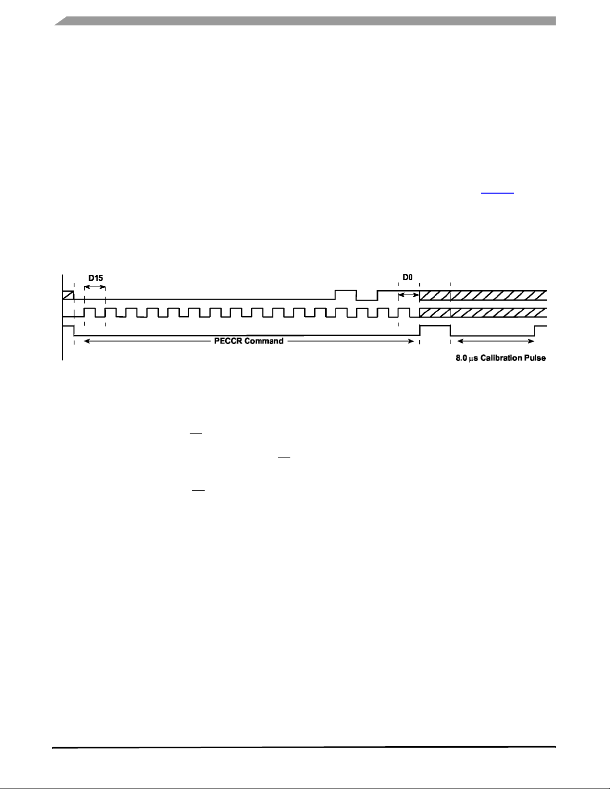
Calibrating the internal 1.0 MHz clock is initiated by writing
Logic [1] to PECCR bit PE3, illustrated in
Figure 8.
Figure 8. Gauge Enable and Clock Calibration Example
The 8.0 µs calibration pulse is then provided by the
controller to result in a nominal internal 33977 clock speed of
1.0 MHz. The pulse is sent on the
CS pin immediately after
the SPI calibration command is sent. During the calibration,
no other SPI lines should be toggled. At the moment the CS
pin transitions from Logic [1] to Logic [0], an internal 7-bit
counter counts the number of cycles of an internal, 8.0 MHz
clock. The counter stops when the
CS pin transitions from
Logic [0] to Logic [1]. The value in the counter represents the
number of cycles of the 8.0 MHz clock occurring in the 8.0 µs
window; it should range from 32 to 119. An offset is added to
this number to help center, or skew, the calibrated result to
generate a desired maximum, or normal frequency. The
modified counter value is truncated by four bits to generate
the calibration divisor, potentially ranging from four to 15. The
8.0 MHz clock is divided by the calibration divisor, resulting in
a calibrated 1.0 MHz clock. If the calibration divisor lies
outside the range of four to 15, the 33977 flags the CAL bit in
the device Status register, indicating the calibration
procedure was not successful. A clock calibration is allowed
only if the gauge is disabled, or the pointer is not moving as
indicated by the Status bit of MOV, illustrated in
Table 16
section of this document.
Some applications may require a guaranteed maximum
pointer velocity and acceleration. Guaranteeing these
maximums requires the nominal internal clock frequency to
fall below 1.0 MHz. The frequency range of the calibrated
clock is always below 1.0 MHz if PECCR bit PE4 is Logic [0]
prior to initiating a calibration command, followed by an 8.0 µs
reference pulse. The frequency is centered at 1.0 MHz if bit
D4 is written Logic [1].
The 33977 can be fooled into calibrating faster or slower
than the optimal frequency by sending a calibration pulse
longer or shorter than the intended 8.0 µs. As long as the
calibration divisor remains between four and 15 there is no
calibration flag. For applications requiring a slower calibrated
clock, e.g., a motor designed with a gear ratio of 120:1
microsteps/deg), users will have to provide a longer
(8
calibration pulse. The internal oscillator can be slowed with
the PECCR command, so the calibration divisor safely falls
within the four to 15 range when calibrating with a longer time
reference. Fro example, for the 120:1 motor, the pulse would
be 12 µs instead of 8.0 µs. The result of this slower calibration
is longer step times resulting in generating pointer
movements capable of meeting acceleration and velocity
requirements. The resolution of the pointer positioning
decreases from 0.083 deg/microstep (180:1) to 0.125
deg/microstep (120:1) while the pointer sweep range
increases from approximately 340° to over 500°.
Note: A fast calibration could result in violations of the
motor acceleration and a velocity maximums, resulting in
missed steps.
33977
Analog Integrated Circuit Device Data
16 Freescale Semiconductor
Page 17
FUNCTIONAL DEVICE OPERATION
OPERATIONAL MODES
POINTER DECELERATION
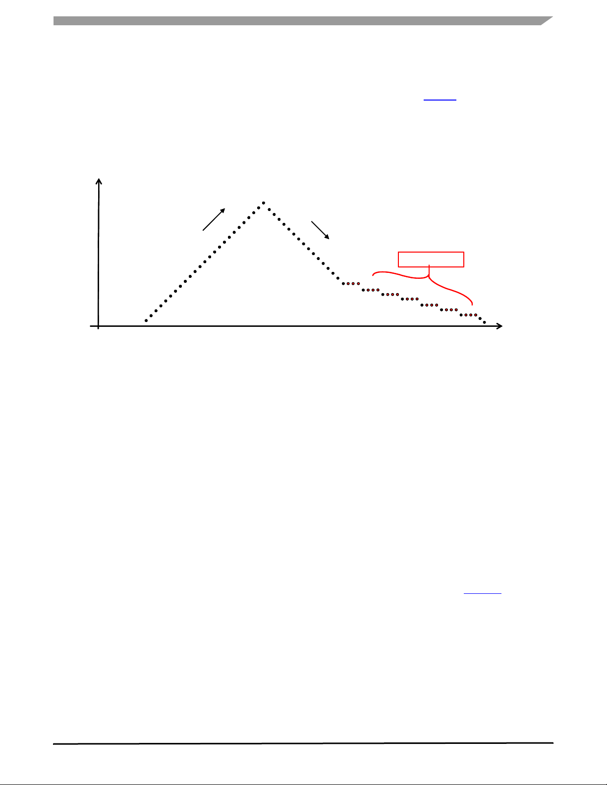
Constant acceleration and deceleration of the pointer
produces relatively choppy movements when compared to
those of an air core gauge. Modification of the velocity
position ramp during deceleration can create the desired
damped movement. This modification is accomplished in the
33977 by adding repetitive steps at several of the last velocity
.
D
D
e
Velocity
Velocity
Position
Position
Position
Position
Position
=
= 0
=
22
22
22
22
21
21
21
21
20
20
20
20
19
19
19
19
18
18
18
18
17
17
17
17
16
16
16
16
15
15
15
15
rate
rate
14
14
14
14
le
le
13
13
13
13
12
12
12
12
ce
ce
c
c
11
11
11
11
A
A
10
10
10
10
9
9
9
9
8
8
8
8
7
7
7
7
6
6
6
6
5
5
5
5
4
4
4
4
3
3
3
3
2
2
2
2
1
1
1
1
0
0
0
Figure 8. Deceleration Ramp
Figure 8. Deceleration Ramp
e
c
c
24
24
24
24
24
24
24
23
23
23
23
23
23
23
22
22
22
position step values as the pointer decelerates. The default
movement in the 33977 uses this ramp modification feature.
An example is illustrated in
Figure 9. If the maximum
acceleration and deceleration of the pointer is desired, the
repetitive steps can be disabled by writing Logic [1] to the
PECCR bit PE5.
e
e
l
l
e
e
r
r
a
a
t
t
e
e
21
21
21
20
20
20
19
19
19
18
18
18
17
17
17
16
16
16
15
15
15
14
14
14
13
13
13
12
12
12
11
11
11
10
10
10
9
9
9
8
8
7
7
Hold Counts
Hold Counts
6
6
5
5
4
4
3
3
2
2
1
1
0
0
Microsteps
Microsteps
Figure 9. Deceleration Ramp
RETURN TO ZERO CALIBRATION
Many stepper motor applications require [that deleted as
PV] the IC detect when the stepper motor stalls after
commanded to return to the zero position for calibration
purposes. In instrumentation applications, the stalling occurs
when the pointer hits the end stop on the gauge bezel,
[which is deleted as PV] usually at the zero position. It is
important to know [that PV] when the pointer reaches the end
stop, it immediately stops without bouncing away. The 33977
device provides the ability to automatically and independently
return the pointer to the zero position via the RTZR and
RTZCR SPI commands. An automatic RTZ is initiated, using
the RZ1 and RZ2 bits, provided the RZ4 is Logic [1]. During
an RTZ event, all commands related to the gauge being
returned are ignored until the pointer has successfully
zeroed, or the RTZR bit RZ1 is written to disable the event.
Once an RTZ event is initiated, the device reports back via
the SO pin an RTZ event is underway.
The RTZCR command is used to set the RTZ pointer
speed, choose an appropriate blanking time, and preload the
integration accumulator with an appropriate offset. On
reaching the end stop, the device reports back to the
microcontroller via the status message [that PV] the RTZ was
successful. The RTZ automatically disables, [that will PV]
allowing other commands to be valid. In the event the master
determines an RTZ sequence is not working properly, for
example, the RTZ taking too long; it can disable the
command via the RTZR bit RZ1. [Altered for better read flow]
RTZCR bits RC10:RC5 are written to preload the
accumulator with a predetermined value assuring accurate
pointer stall detection. This preloaded value can be
determined during application development by disabling the
automatic shutdown feature of the device with the RTZR bit
RZ4. This operating mode allows the master to monitor the
RTZ event, using the accumulator information available via
the SO if the device is configured to provide the RTZ
Accumulator Status. The unconditional RTZ event can be
turned OFF using the RTZR bit RZ1.
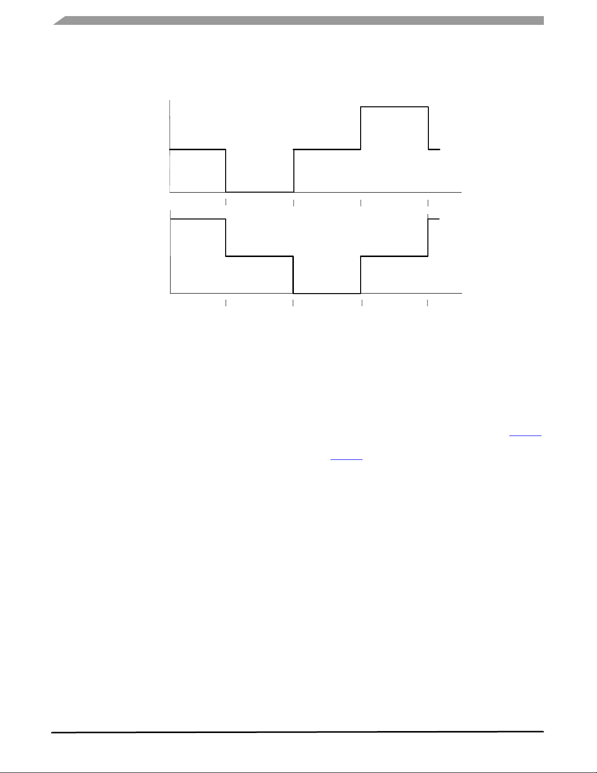
If the Position 0 location bit, RZ2, is in the default Logic [0]
mode, then during an RTZ event the pointer is returned
counterclockwise (CCW) using full steps at a constant speed
determined by the RTZCR RC3:RC0 and RC12:RC11 bits
written during RTZ configuration, see
Figure 10. Full steps
are used during an RTZ so only coil of the motor is being
driven at any time. The coil not being driven is used to
determine if the pointer is moving. If the pointer is moving, the
flux present in the non-driven coil is processed by integrating
the back EMF signal present on the opened pin of the coil
while applying a fixed potential to the other end.
33977
Analog Integrated Circuit Device Data
Freescale Semiconductor 17
Page 18
FUNCTIONAL DEVICE OPERATION
OPERATIONAL MODES
I
I
max
MAX
+
I
coil
I
COIL
0
_
I
MAX
I
max
I
I
MAX
max
SINE
2 0 0 3 1
I
COIL
I
coil
+
0
_
I
MAX
I
max
0 1 2 3 0
Figure 9. FULLSTEPS (Counter Clockwise)
Figure 10. Full Steps (Counterclockwise)
The IC automatically prepares the non-driven coil at each
step, waits for a predetermined blanking time, and then
processes the signal for the duration of the full step. When
the pointer reaches the stop and not longer moves, the
dissipating flux is detected. The processed results are placed
in the RTZ accumulator, and then compared to a decision
threshold. If the signal exceeds the decision threshold, the
pointer is assumed to be moving. If the threshold value is not
exceeded, the drive sequence is stopped if RTZR bit RZ4 is
Logic [0]. If bit RZ4 is Logic [1], the RTZ movement will
continue indefinitely until the RTZR bit RZ1 is used to stop the
RTZ event.
A pointer [that is PV] not on a full step location, or [that
PV] is in magnetic alignment prior to the RTZ event may
cause a false RTZ detection. More specifically, an RTZ event
beginning from a non-full step position may result in an
abbreviated flux value potentially interpreted as a stalled
pointer. Advancing the pointed by at least 12 microsteps
clockwise (if PE7 = 0) to the nearest full step position (e.g., 0,
6, 12, 18, 24, etc.) prior to initiating an RTZ ensures the
magnetic fields line up and increases the chances of a
successful pointer stall detection. It is important that the
pointer be in a static, or commanded, position before starting
the RTZ event. Because the time duration and the number of
steps the pointer moves prior to reaching the commanded
position can vary depending upon its status at the time a
position change is communicated, the master should make
sure that the rotor is not moving prior to starting an RTZ.
Cessation of movement can be inferred by monitoring the
CMD and/or the MOV status bits.
It should be pointed out, the flux value, for an ideal motor
with the coils perfectly aligned at 90°, will vary little from full
step to full step if all other variables, such as te mperature, are
COSINE
held constant. The full steps are evenly spaced, resulting in
equidistant movement as the motor is full stepped.
In comparison, motors [that have deleted PV] whose coils
aligned at a 60° angle [will deleted PV] results in two distinct
flux values as a the coils are driven in the same full step
fashion. This lack of symmetry in the measured flux is due to
the difference in the electrical angles between full steps.
Clearly stated, the distance the rotor moves changes from full
step to full step. This difference can be observed in
Figure 7
and Table 5.
In Figure 7, where PE6 = 0, the difference in microsteps
between alternating full steps (one coil at maximum current
while the other is at zero) is always six. In contrast, the same
figure illustrates PE6 = 1 showing the dif fe ren ce in
microsteps between full steps of the 60° coils alternating
between four and eight. These expected differences should
be taken into account when setting the RTZ threshold.
After completion of an RTZ, the 33977 automatically
assigns the zero step position to the full step position at the
end-stop location. Because the actual zero position could lie
anywhere within the full step where the zero was detected,
the assigned zero position could be within a window of ±0.5°.
An RTZ can be used to detect stall, even if the pointer rests
on the end-stop when RTZ sequence is initiated. However, it
is recommended to advance the pointer by at least 12
microsteps to the nearest full step prior to initiating the RTZ.
RTZ OUTPUT
During an RTZ event the non-driven coil is analyzed to
determine the state of the motor. The 33977 multiplexes the
coil voltages, [chgd PV and provides to read as active voice]
providing signal from the non-driven coil to the RTZ pin.
33977
Analog Integrated Circuit Device Data
18 Freescale Semiconductor
Page 19

FUNCTIONAL DEVICE OPERATION
OPERATIONAL MODES
DEFAULT MODE
Default mode refers to the state of the 33977 after an
internal or external reset prior to SPI communication. An
internal reset occurs during V
power-up or if V
DD
PWR
falls
below 4.0 V. An external reset is initiated by the RST pin
driven to Logic [0]. With the exception of the RTZCR full step
time, all of the specific pin functions and internal registers will
operate as though all of the addressable configuration
register bits were set to Logic [0]. This means, for example,
[deleted PV that] the outputs will be disabled after a powerup or external reset, and SO flag OD6 and OD8 are set,
indicating an undervoltage event. Anytime an external reset
is exerted and the default is restored, all configuration
parameters [replaced e.g. with such as] such as clock
calibration, maximum speed, and RTZ parameters are lost
and must be reloaded.
FAULT LOGIC REQUIREMENTS
The 33977 device indicates each of the following faults as
they occur:
• Overtemperature fault
• Undervoltage V
• Overvoltage V
PWR
PWR
• Clock Out of Specification [Formalized spec]
These fault bits remain enabled until they are clocked out
of the SO pin with a valid SPI message.
Overcurrent faults are not reports directly; however, it is
likely an overcurrent condition will become a thermal issue
and be reported.
OVERTEMPERATURE FAULT REQUIREMENTS
The 33977 incorporates overtemperature protection
circuitry, shutting off the gauge driver when an excessive
temperature is detected. In the event of a thermal overload,
the gauge driver is automatically disabled and the fault is
flagged via the OT device status bit. The indicating flag
continues to be set until the gauge is successfully re-enacted,
provided the junction temperature has fallen below th e
hysteresis level.
OVERVOLTAGE FAULT REQUIREMENTS
The device is capable of surviving V
the maximum specified in Maximum Ratings,
levels resulting in an overvoltage shutdown condition can
result in uncertain pointer positions. Therefore, the pointer
position should be re-calibrated. The master will be notified of
an overvoltage event via the SO pin if the device status is
selected. Overvoltage detection and notification occurs
regardless of whether the gauge(s) are enabled or disabled.
voltages within
PWR
Table 2. V
PWR
OVERCURRENT FAULT REQUIREMENTS
Outcome currents are limited to safe levels allowing the
device to rely on thermal shutdown to protect itself.
UNDERVOLTAGE FAULT REQUIREMENTS
Undervoltage V
pointer positions. Therefore, the internal clock and the pointer
position may require re-calibration. The state machine
continues to operate with V
V; however, the coil voltages may be clipped. Notification of
an undervoltage event is provided via the SO pin.
conditions may result in uncertain
PWR
voltage levels as low as 4.0
PWR
RESET (SLEEP MODE)
The device can reset internally or externally. If the VDD
level falls below the V
powers up in the Default mode. See Static Electrical
Characteristics table under the sub-heading: Power Input in
Table 3. Similarly, if the RST pin is driven to Logic [0], then
the device resets to its default state. The device consumes
the least amount of current (IDD and I
is Logic [0]. This is also referred to as the Sleep mode.
level, the device resets and
DDUV
) when the RST pin
PWR
33977
Analog Integrated Circuit Device Data
Freescale Semiconductor 19
Page 20

FUNCTIONAL DEVICE OPERATION
LOGIC COMMANDS AND REGISTERS
LOGIC COMMANDS AND REGISTERS
SPI PROTOCOL DESCRIPTION
The SPI interface has a full-duplex, three-wire
synchronous,16-bit serial synchronous interface data
transfer and four I/O lines associated with it: Chip Select
CS), Serial Clock (SCLK), Serial Input (SI), and Serial Output
(
(SO). The SI/SO pins of the 33977 follow a first in/first out
(D15/D0) protocol with both input and output words
transferring the most significant bit first. All inputs are
compatible with 5.0 V CMOS logic levels.
CHIP SELECT (CS)
The CS pin enables communication with the master
device.
When this pin is in a Logic [0] state, the 33977 is capable
of transferring information to, and receiving information from,
the master. The 33977 latches data in from the Input Shift
registers to the addressed registers on the rising edge of
The output driver on the SO pin is enabled when
CS.
CS is Logic
[0]. When CS is logic high, signals at the SCLK and SI pins
are ignored and the SO pin is tri-stated (high impedance). CS
will only be transitioned from a Logic [1] state to a Logic [0]
state when SCLK is Logic [0]. CS has an internal pull-up (IUP)
connected to the pin, as specified in the section of the Static
Electrical Characteristics table entitled CONTROL I/O,
[which is found on page...deleted for consistent format]
Table 3. This pin is also used to calibrate the internal clock.
SERIAL CLOCK (SCLK)
SCLK clocks the Internal Shift registers of the 33977
device. The SI pin accepts data into the Input Shift register on
the falling edge of the SCLK signal, while the Serial Output
pin (SO) shifts data information out of the SO line driver on
the rising edge of the SCLK signal. It is important the SCLK
pin be in a Logic [0] state whenever the
transition. SCLK has an internal pull-down (l
specified in the section Control I/O of the Static Electrical
Characteristics, [which is found on page...deleted for
consistent format]
Table 3. When CS is Logic [1], signals at
the SCLK and SI pins are ignored and SO is tri-stated (high
impedance). Refer to the data transfer timing diagrams in
CS makes any
), as
DWN
Figure 11 and Figure 12. [figure numbers changed due to
template formatting]
It transitions one time per bit transferred at an operating
frequency, f
the Dynamic Electrical Characteristics
, defined in the SPI Interface Timing section of
SPI
Table 4. It is idle
between command transfers. The pin is 50 percent duty
cycle, with CMOS logic levels. This signal is used to shift data
to and from the device.
SERIAL OUTPUT (SO)
The SO data pin is a tri-stateable output from the Shift
register. This output will remain tri-stated unless the device is
selected by a low
CS signal. The output signal generated will
have CMOS logic levels and the output will transition on the
rising edges of SCLK. The serial output data provides status
feedback and fault information for each output and is returned
MSB first when the device is addressed.
The Status register bits are the first 16 bits shifted out.
Those bits are followed by the message bits clocked in FIFO,
when the device is in a daisy chain connection, or being sent
words [that are deleted as PV] multiples of 16 bits. Data is
shifted on the rising edge of the SCLK signal. The SO pin
[will deleted as PV] remains in a high impedance state until
CS pin is put into a logic low state.
the
SERIAL INPUT (SI)
The SI pin is the input of the SPI. This input has an internal
active pull-down requiring CMOS logic levels. The serial data
transmitted on this line is a 16-bit co ntrol command sent MSB
first, controlling the gauge functions. The master ensures
data is available on the falling edge of SCLK.
Serial input information is read on the falling edge of
SCLK. A 16-bit stream of serial data is required on the SI pin,
beginning with the most significant bit (MSB). Messages [that
are deleted as PV] not multiples of 16 bits (e.g., daisy
chained device messages) are ignored. After transmitting a
16-bit word, the
transmitting a new word. SI information is ignored when CS
is in a logic high state.
CS pin must be de-asserted (Logic [1]) before
33977
Analog Integrated Circuit Device Data
20 Freescale Semiconductor
Page 21
FUNCTIONAL DEVICE OPERATION
LOGIC COMMANDS AND REGISTERS
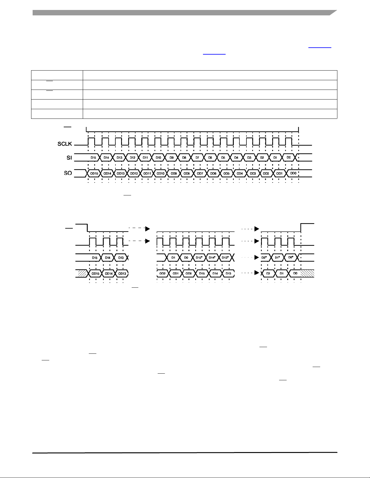
This section provides a description of the 33977 SPI
behavior. To follow the explanation below, please refer to
Table 7 and to the timing diagrams illustrated in Figure 11
and Figure 12.
Table 7. Data Transfer Timing
Pin
CS (1-to-0) SO pin is enabled
CS (0-to-1) 33977 configuration and desired output states are transferred and executed according to the data in the Shift registers
SO Will change state on the rising edge of the SCLK pin signal
SI Will accept data on the falling edge of the SCLK pin signal
Description
CS
Output Shift register is loaded here
Note: SO is tri-stated when CS
is Logic [1]
Figure 11. Single 16-Bit Word SPI Communication
CS
SCLK
SI
SO
Notes:
1. SO is tri-stated when CS
2. D15, D14, D13, , and D0 refer to the first 16 bits of data into the 33977.
3. D15*, D14*, D13*,. . . ., and D0* refer to the most recent entry of program data into the 33977.
4. OD15, OD14, OD13, . . .,and OD0 refer to the first 16 bits of fault and status data out of the 33977.
D12 D11
0D12 OD
is Logic [1].
D2
Figure 12. Multiple 16-Bit Word SPI Communication
DATA INPUT
The Input Shift register captures data at the falling edge of
the SCLK. The SCLK pulses exactly 16 times only inside the
transmission windows (
the
CS signal goes to Logic [1] again, the contents of the
Input Shift register are transferred to the appropriate internal
register addressed in bits 15:13. The minimum time
should be kept high depends on the internal clock speed,
specified in the SPI Interface Timing section of the [Static
replaced with Dynamic - correcting table location] Dynamic
Electrical Characteristics,
the internal clock is able to capture the data from the Input
Shift register and transfer it to the internal regist ers.
CS in a Logic [1] state). By the time
CS
Table 4. It must be long enough so
DATA OUTPUT
At the first rising edge of the SCLK [clock deleted to
eliminate redundancy], with
CS at Logic [1], the contents of
the selected Status Word register are transferred to the
Output Shift register. The first 16 bits clocked out are the
status bits. If data continues to clock in before the
CS
transitions to Logic [1], the device begins to shift out the data
previously clocked in FIFO after the
CS first transitioned to
Logic[1].
COMMUNICATION MEMORY MAPS AND
REGISTER DESCRIPTIONS
The 33977 device is capable of interfacing directly with a
microcontroller via the 16-bit SPI protocol specified below.
33977
Analog Integrated Circuit Device Data
Freescale Semiconductor 21
Page 22

FUNCTIONAL DEVICE OPERATION
LOGIC COMMANDS AND REGISTERS
The device is controlled by the microprocessor and reports
back status information via the SPI. This section provides a
detailed description of all registers accessible via serial
interface. The various registers control the behavior of this
device.
A message is transmitted by the master beginning with the
MSB (D15) and ending with the LSB (D0). Multiple messages
can be transmitted in succession to accommodate those
applications where daisy chaining is desirable, or to confirm
transmitted data, as long as the messages are all multiples of
16 bits. Data is transferred through daisy-chained devices, as
illustrated in
Figure 12. If an attempt is made to latch in a
message smaller than 16 bits wide, it is ignored.
Table 8 lists the five registers the 33977 uses to configure
the device, control the state of the [Chgd to two per D.
Mortensen] two H-bridge outputs, and determine the type of
status information [that is deleted PV] clocked back to the
master. The registers are addressed via D15:D13 of the
incoming SPI word.
Table 8. Module Memory Map
Address
[15:13]
000 Power, Enable, Calibration, and
Configuration Register
001 Maximum Velocity Register
010 Gauge Position Register
011 Not Used
100 Return to Zero Register
101 Return to Zero Configuration
Register
110 Not Used
111 Reserved for Test
[The word Zero omitted above in 101 my error]
MODULE MEMORY MAP
Various registers of the 33977 SPI module are addressed
by the three MSBs of the 16-bit word received serially.
Functions to be controlled include:
• Individual gauge drive enabling
• Power-up/down
• Internal clock calibration
• Gauge pointer position and velocity
• Gauge pointer zeroing
• Air core motor movement emulation
• Status information
Status reporting includes:
• Individual gauge overtemperature condition
Register Name See
PECCR Table
9
VELR Table
10
POSR Table
11
– –
RTZR Table
12
RTZCR Table
13
RMPSELR –
– –
• Battery overvoltage
• Battery undervoltage
• Pointer zeroing status
• Internal clock status
• Confirmation of pointer movement commands
• Real time pointer position information
• Real time pointer velocity step information
• Pointer movement direction
• Command pointer position status
• RTZ accumulator value
REGISTER DESCRIPTIONS
The following section describes the registers, their
addresses, and their impact on device operation.
ADDRESS 000 - POWER, ENABLE, CALIBRATION,
AND CONFIGURATION REGISTER (PECCR)
The Power, Enable, Calibration, and Configuration
Register is illustrated in
this register allows the master to:
• Enable or disable the output drivers of the gauge
controller
• Calibrate the internal clock
• Disable the air core emulation
• Select the direction of the pointer movement during
pointer positioning and zeroing
• Configure the device for the desired status information
to be clocked out into the SO pin, or
• Send a null command for the purpose of reading the
status bits.
This register is also used to place the 33977 into a low
current consumption mode.
The gauge drivers can be enabled by writing Logic [1] to
the assigned address bits, PE0. This feature could be used
to disable a driver if it is failing. The device can be placed into
a standby current mode by writing Logic [0] to PE0. During
this state, most current consuming circuits are biased off.
When in the Standby mode, the internal clock will remain ON.
The internal state machine utilizes a ROM table of step
times defining the duration that the motor will spend at each
microstep as it accelerates or decelerates to a commanded
position. The accuracy of the acceleration and velocity of the
motor is directly related to the accuracy of the internal clock
Although the accuracy of the internal clock is temperature
independent, the non-calibrated tolerance is +70% to -35%.
The 33977 was designed with a feature allowing the internal
clock to be software calibrated to a tighter tolerance of ±10%,
using the
CS pin and a reference time pulse provided by the
microcontroller.
Calibration of the internal clock is initiated by writing Logic
[1] to PE3. The calibration pulse, which must be 8.0 µs for an
internal clock speed of 1.0 MHz, will be sent on the
immediately after the SPI word is sent. No other SPI lines will
be toggled. A clock calibration will be allowed only if the
gauge is disabled or the pointer is not moving, as indicated
Table 9. A write to the 33977 using
CS pin
33977
Analog Integrated Circuit Device Data
22 Freescale Semiconductor
Page 23

FUNCTIONAL DEVICE OPERATION
LOGIC COMMANDS AND REGISTERS
by status bits MOV0. Additional details are provided in the
Internal clock Calibration section.
Some applications may require a guaranteed maximum
pointer velocity and acceleration. Guaranteeing these fall
below 1.0 MHz. The frequency range of the calibrated clock
maximums requires [that deleted PV] the nominal internal
clock frequency will always be below 1.0 MHz if bit PE4 is
Logic [0] when initiating a calibration command, followed by
µs reference pulse. The frequency will be centered at
an 8.0
1.0 MHz if bit PE4 is Logic [1]. Some applications may require
a slower calibrated clock due to a lower motor gear reduction
ratio. Writing Logic [1] to bit PE2 will slow the internal
oscillator by one-third. Slowing the oscillator accommodates
a longer calibration pulse without overrunning the internal
counter - a condition designed to generate a CAL fault
indication. For example, calibration for a clock frequency of
667 kHz would require a calibration pulse of 12
µs. Unless the
internal oscillator is slowed by writing PE2 to Logic [1], a 12
µs calibration pulse may overrun the counter and generate a
CAL fault indication.
Some applications may require faster pointer positioning
than is provided with the air core motor emulation feature.
Writing Logic [1] to bit PE5 will disable the air core emulation
for both gauges and provide an acceleration and deceleration
at the maximum that the velocity position ramp can provide.
Bit PE6 must always be written Logic [0] during all PECCR
writes if the device is being used to drive an MMT style motor.
Similarly, this bit must always be written as Logic [1] when
being used to control Switec style motors.
The default Pointer Position 0 (PE7 = 0) will be the farthest
counter-clockwise position. A Logic [1] written to bit PE7 will
change the location of the position 0 for the gauge to the
farthest clockwise position. The pointer will always move
towards position 0 when executing an RTZ. Exercise care
when writing to PECCR bit PE7 in order to prevent an
accidental change of the position 0 location.
Bits PE11:PE9 determine the content of the bits clocked
out of the SO pin. When bit PE11 is at Logic [0], the clocked
out bits will provide device status. If Logic [1] is written to bit
PE11, the bits clocked out of the SO pin, depending upon the
state of bits PE10:PE9, provides either:
• Accumulator information and detection status during
the RTZ (PE10 Logic [0])
• Real time pointer position location at the time CS goes
low (PE10 Logic [1] and PE9 Logic [0]), or
• The real time step position of the pointer as described
in the velocity Table 6 (PE10 and PE9 Logic [1]).
Additional details are provided in the SO Communication
section.
If bit PE12 is Logic [1] during a PECCR command, the
state of PE11:PE0 is ignored. This is referred to as the null
command and can be used to read device status without
affecting device operation.
Table 9. Power, Enable, Calibration, and Configuration Register (PECCR)
Address 000
Bits
Read
Write
D12 D11 D10 D9 D8 D7 D6 D5 D4 D3 D2 D1 D0
– – – – – – – – – – – – –
PE12 PE11 PE10 PE9 0 PE7 PE6 PE5 PE4 PE3 PE2 0 PE0
The bits in Table 9 are write-only.
Pointer Position or Pointer Speed Select (PE9) Bit D9
This bit is recognized only if PE11 and PE10 = 1.
Null Command for Status Read (PE12) Bit D12
• 0 = Disable
• 0 = Gauge Pointer Position
• 1 = Gauge Pointer Speed
• 1 = Enable
(PE8) Bit D8
Status Select (PE11) Bit D11
This bit selects the information clocked out of the SO pin.
• 0 = Device Status (the logic states of PE10, and PE9
are don’t cares)
• 1 = RTZ Accumulator Value, Gauge Pointer position, or
Gauge Velocity ramp position (depending upon the
logic states of PE10, and PE9)
This bit must be transmitted as Logic [0] for valid PECCR
commands.
Position 0 Location Select (PE7) Bit D7
This bit determines the Position 0 of the gauge. RTZ
direction will always be to the position 0.
• 0 = Position 0 is the most CCW (counterclockwise)
position
RTZ Accumulator or Pointer Status Select (PE10) Bit D10
• 1 = Position 0 is the most CW (clockwise) position
This bit is recognized only when PE11 = 1.
• 0 = RTZ Accumulator Value and status
• 1 = Pointer Position or Speed
Motor Type Selection (PE6) Bit D6
• 0 = MMT Style (coil phase difference = 90°)
• 1 = Switec Style (coil phase difference = 60°)
33977
Analog Integrated Circuit Device Data
Freescale Semiconductor 23
Page 24

FUNCTIONAL DEVICE OPERATION
LOGIC COMMANDS AND REGISTERS
Air Core Motor Emulation (PE5) Bit D5
This bit is enabled or disabled (acceleration and
deceleration is constant if disabled).
• 0 = Enable
• 1 = Disable
Clock Calibration Frequency Selector (PE4) Bit D4
• 0 = Maximum f =1.0 MHz (for 8.0 µs calibration pulse)
• 1 = Nominal f =1.0 MHz (for 8.0 µs calibration pulse)
Clock Calibration Enable (PE3) Bit D3
This bit enables or disables the clock calibration.
• 0 = Disable
• 1 = Enable
Oscillator Adjustment (PE2) Bit D2
•0 = t
CLU
• 1 = 0.66 x t
CLU
(PE1) Bit D1
This bit must be transmitted as Logic [0] for valid PECCR
commands
Table 10. Maximum Velocity Register (VELR)
Gauge Enable (PE0) Bit D0
This bit enables or disables the output drivers of the
Gauge.
• 0 = Disable
•1 = Enable
ADDRESS 001 - MAXIMUM VELOCITY REGISTER
(VELR)
The Gauge Maximum Velocity Register is used to set a
maximum velocity for the gauge (refer to
contain a position value from 1 - 225 representative of the
velocity position value described in the Velocity Table,
Table 6. The table value becomes the maximum velocity until
it is changed to another value. If a maximum value is chosen
that is greater than the maximum velocity of the acceleration
table, the maximum table value becomes the maximum
velocity.
If the motor is turning at a speed greater than the new
maximum, the motor immediately moves down the velocity
ramp until the speed falls equal to or below it. Bit V8 must be
written to a Logic [1] when changing the maximum velocity of
the motor. Bits V12:V10 must be at Logic [0] for valid VELR
commands.
.
Table 4). Bits V7:V0
Bits
Read
Write
D12 D11 D10 D9 D8 D7 D6 D5 D4 D3 D2 D1 D0
– – – – – – – – – – – – –
0 0 0 0 V8 V7 V6 V5 V4 V3 V2 V1 V0
The bits in Table 10 are write-only.
(V12:V9) Bits D12:D9
These bits must be transmitted as Logic [0] for valid VELR
commands.
Gauge Velocity (V8) Bit D8
Enables the maximum velocity as determined in the V7:
V0.
• 0 = Velocity change disabled
• 1 = Velocity change enabled
Table 11. Gauge Position Register (POSR)
Bits
Read
Write
D12 D11 D10 D9 D8 D7 D6 D5 D4 D3 D2 D1 D0
– – – – – – – – – – – – –
0 P011 P010 P09 P08 P07 P06 P05 P04 P03 P02 P01 P00
The bits in Table 11 are write-only.
Address 001
(V7:V0) Bits D7:D0
These bits can be used to program the device to limit the
maximum velocity of the pointer movement. to one of over
200 speeds listed in the Velocity Table 6. This velocity will
remain the maximum of the intended gauge until changed by
command. Velocities can range from position 1 (00000001)
to position 225 (11111111).
ADDRESSES 010 - GAUGE POSITION REGISTER
(POSR)
SI Address 010 (Gauge Position Register) register bits
PO11: PO0 are written to when communicating the desired
pointer positions. Commanded positions can range from 0 to
4095
Address 010
33977
Analog Integrated Circuit Device Data
24 Freescale Semiconductor
Page 25

FUNCTIONAL DEVICE OPERATION
LOGIC COMMANDS AND REGISTERS
PO012 (D12)
This bits must be transmitted as Logic [0] for valid POSR
commands.
P011:P00 (D11:D0)
Desired pointer position of Gauge. Pointer positions can
range from 0 (000000000000) to position 4095
(111111111111). For a stepper motor requiring 12
microsteps per degree of pointer movement, the maximum
pointer sweep is 341.25° (4095 ÷ 12).
ADDRESS 100 - GAUGE RETURN TO ZERO
REGISTER (RTZR)
Gauge Return to Zero Register (RTZR), Table 12 below,
is written to return the gauge pointers to the zero position.
During an RTZ event, the pointer is returned to zero using full
Table 12. Gauge Return to Zero Register (RTZR)
Address 100
Bits
Read
Write
The register bits in Table 12 are write-only.
(RZ12:RZ5) Bits D12:D5
These bits must be transmitted as Logic [0] for valid
commands.
(RZ4) Bit D4
This bit is used to enable an unconditional RTZ event.
• 0 = Automatic Return to Zero
• 1 = Unconditional Return to Zero
(RZ3) Bit D3
This bit must be transmitted as Logic [0] for val i d
commands.
(RZ2) Bit D2
Return to Zero Direction bit. This bit is used to properly
sequence the integrator, depending upon the desired zeroing
direction.
• 0 = Return to Zero will occur in the CCW direction
• 1 = Return to Zero will occur in the CW direction
(RZ1) Bit D1
Return to Zero Enable. This bit commands the gauge to
return the pointer to zero position.
• 0 = Return to Zero Disabled
• 1 = Return to Zero Enabled
D12 D11 D10 D9 D8 D7 D6 D5 D4 D3 D2 D1 D0
– – – – – – – – – – – – –
0 0 0 0 0 0 0 0 RZ4 0 RZ2 RZ1 0
(PE7 = 0)
=1)
(PE7
steps, where only one coil is driven at any point in time. The
back electromotive force (EMF) signal present on the nondriven coil is integrated and its results are stored in an
accumulator. A Logic [1] written to bit RZ1 enables a Return
to Zero for the Gauge if RZ0 is Logic [0]. A Logic [0] written to
bit RZ1 disables a Return to Zero for the Gauge when RZ0 is
Logic [0].
Bits D12:D5 and D3:D2 must be written Logic [0] for valid
RTZR commands. An unconditional RTZ event can be
enabled or disabled with Bit RZ4. Writing Logic [0] results in
a typical RTZ event, automatically providing a Stop when a
stall condition is detected. A Logic [1] will result in RTZ
movement, causing a Stop if a Logic [0] is written to bit RZ0.
This feature is useful during development and
characterization of RTZ requirements.
(RZ0) Bit D0
Return to Zero Enable. This bit must always be written
Logic [0].
ADDRESS 101 - GAUGE RETURN TO ZERO
CONFIGURATION REGISTER
Gauge Return to Zero Configuration Register (RTZCR) is
used to configure the Return to Zero Event, Table 13. It is
written to modify the: [listed as bullets for reading ease]
• Step time, or rate at which the pointer moves during an
RTZ event
• Integration blanking time, which is the time immediately
following the transition of a coil from a driven state to an
open state in the RTZ mode
• Threshold of the RTZ integration register
Values used for this register should be selected during
development to optimize the RTZ for each application.
Selecting an RTZ step rate resulting in consistently
successful zero detections depends on a clear understanding
of the motor characteristics. Specifically, resonant
frequencies exist due to the interaction between the motor
and the pointer. This command allows for the selection of an
RTZ pointer speed away from these frequencies. Also, some
motors require a significant amount of time for the pointer to
settle to a steady state position when moving from one full
step position to the next. Consistent and accurate integration
values require that the pointer be stationary at the end of the
full step time.
Bits RC3:RC0, RC12:RC11, and RC4 determine the time
spent at each full step during an RTZ event. Bits RC3:RC0
are used to select a ∆t ranging from 0 ms (0000) to 61.44 ms
33977
Analog Integrated Circuit Device Data
Freescale Semiconductor 25
Page 26

FUNCTIONAL DEVICE OPERATION
LOGIC COMMANDS AND REGISTERS
(1111) in increments of 4.096 ms (refer to Table 14). The ∆t
is multiplied by the factor M, defined by bits RC12:RC11. The
product is then added to the blanking time, selected using bit
RC4, to generate the full step time. The multiplier selected
with RC12:RC11 will be 1
(00), 2 (01), or 4 (10) as illustrated
in the equations below. Note that the RC12:RC11 value of 8
(11) is not recommended for use in a product design
application, because of the potential for an RTZ accumulator
internal overflow, due to the long time step. The blanking time
is either 512 µs when RC4 is Logic [0], or 768 µs when it is
Logic [1].The full step time is calculated using the following
equations:
When D3:D0 (RC3:RC0) = 0000
Full Step (t) = ∆t x M+ blanking (t) (1)
When D3:D0 (RC3:RC0) = 0000
Full Step (t) = blanking (t) + 2.048 ms (2)
Note: In equation (2), a 2.048 ms offset is added to the full
step time when the RC3:RC0 = 0000. The full step time
default value after a logic reset is 12.80 ms (RC12:RC11 =
00, RC4 = 0, and RC3:RC0 = 0011).
If there are two full steps per degree of pointer movement,
the pointer speed is 1/(Full Step x 2) deg/s.
Detecting pointer movement is accomplished by
integrating the EMF present in the non-driven coil during the
RTZ event. The integration circuitry is implemented using a
Sigma-Delta converter resulting in the placement of a value
in the 15-bit RTZ accumulator at the end of each full step. The
value in the RTZ accumulator represents the change in flux
and is compared to a threshold. Values above the threshold
indicate a pointer is moving. Values below the threshold
indicate a stalled pointer, thereby resulting in the cessation of
the RTZ event.
two’s complement. After a full step of integration, a sign bit of
0 is the indicator of an accumulator exceeding the decision
threshold of 0, and the pointer is assumed to still be moving.
Similarly, if the sign bit is Logic [1] after a full step of
integration, the accumulator value is negative and the pointer
is assumed to be stopped. The integrator and accumulator
are initialized after each full step. If the PECCR command is
written to clock out the RTZ accumulator values via the SO,
the OD14 bit corresponds to the sign bit of the RTZ
accumulator.
preloaded accumulator for specific gauge, pointer, and full
step combinations. Bits RC10:RC5 are used to offset the
initial RTZ accumulator value, properly detecting a stalled
motor. The initial accumulator value at the start of a full step
of integration is negative. If the accumulator was correctly
preloaded, a free moving pointer will result in a positive value
at the end of the integration time, and a stalled pointer will
result in a negative value. The preloaded values associated
with each combination of bits RC10:RC5 are illustrated in
Table 15. The accumulator should be loaded with a value
resulting in an accumulator MSB to Logic [1] when the motor
is stalled. For the default mode, after a power-up or any reset,
the 33977 device sets the accumulator value to -1.
Table 13. Return to Zero Register Configuration Register (RTZCR)
The RTZ accumulator bits are signed and represented in
Accurate pointer stall detection depends on a correctly
Address 101
Bits
Read
Write
D12 D11 D10 D9 D8 D7 D6 D5 D4 D3 D2 D1 D0
– – – – – – – – – – – – –
RC12 RC11 RC10 RC9 RC8 RC7 RC6 RC5 RC4 RC3 RC2 RC1 RC0
The bits in Table 13 are write-only.
(RC12:RC11) Bits D12:D11
These bits, along with RC3:RC0 (D3:D0) and RC4 (D4),
determine the full step time and, therefore, the rate at which
the pointer will move during an RTZ event. The values of
D12:D11 determine the multiplier (M) used in equation (1)
(refer to the previous page).
RC12:RC11 = M; default value = 00
• 00 = 1
• 01 = 2
• 10 = 4
• 11 = 8 (Not to be used for design)
(RC10:RC5) Bits D10:D5
These bits determine the value preloaded into the RTZ
integration accumulator to adjust the detection threshold.
Values range from -1 (00000000) to -1009 (11111111) as
shown in
Table 15, the default value = 000000.
(RC4) Bit D4
This bit determines the RTZ blanking time (blanking (t)).
The default value = 0
• 0 = 512 µs
• 1 = 768 µs
(RC3:RC0) Bits D3:D0
These bits, along with RC12:RC11 (D12:D11) and RC4
(D4), determine the time variables used to calculate the full
step times with equations (1) or (2) illustrated above.
RC3:RC0 determines the ∆t time. The ∆t values range from 0
(0000) to 61.440 ms (1111) and are shown in
Table 14. The
default ∆t is 0 (0011).
Note: Equation (2) (refer to the preceding page) is only
used to calculate the full step time if RC3:RC0 = 0000. Use
equation (1) for all other combinations of RC3:RC0.
33977
Analog Integrated Circuit Device Data
26 Freescale Semiconductor
Page 27
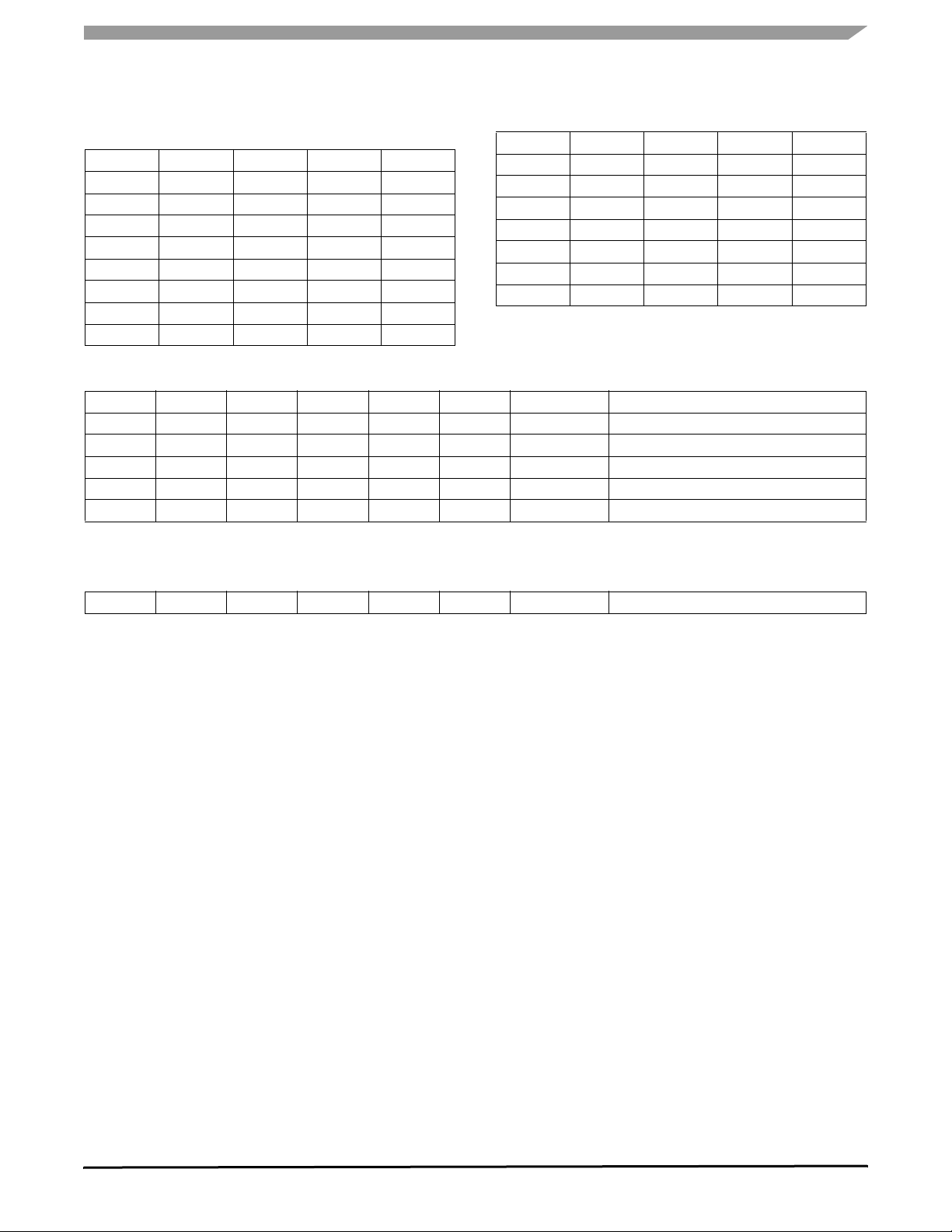
FUNCTIONAL DEVICE OPERATION
LOGIC COMMANDS AND REGISTERS
Table 14. RTZCR Full Step Time
RC3
0 0
0 0
0 0
0 0
0 1
0 1
0 1
0 1
RC2 RC1 RC0 ∆t (ms)
0 0 0.0
0 1 4.096
1 0 8.192
1 1 12.288
0 0 16.384
0 1 20.480
1 0 24.576
1 1 28.672
Table 15. RTZCR Accumulator Offset
RC10
0 0 0 0
0 0 0 0
0 0 0 0
0 0 0 0
0 0 0
. .
. .
. .
1 1
RC9 RC8 RC7 RC6 RC5 Preload Value Initial Accumulator Value = (-16xPV) -1
. . . . . .
. . . . . .
. . . . . .
1 1 1 1 63 -1009
Table 14. RTZCR Full Step Time
1 0
1 0
1 0
1 0
1 1
1 1
1 1
1 1
0 0 0 -1
0 1 1 -17
1 0 2 -33
1 1 3 -49
1 0 0 4 -65
0 0 32.768
0 1 36.864
1 0 40.960
1 1 45.056
0 0 49.152
0 1 53.248
1 0 57.344
1 1 61.440
33977
Analog Integrated Circuit Device Data
Freescale Semiconductor 27
Page 28

FUNCTIONAL DEVICE OPERATION
LOGIC COMMANDS AND REGISTERS
SO COMMUNICATION
When the CS pin is pulled low, the internal status register,
as configured with the PECCR command bits PE11:PE8, is
loaded into the output register and the data is clocked out
MSB (OD15) first. Following a
determines if the shifted-in message was of a valid length (a
valid message length is one that is greater than 0 bits and a
multiple of 16 bits) and, if so, latches the incoming data into
the appropriate registers. At this time, the SO pin is tri-stated
and the status register is now able to accept new status
information. Fault status information will be latched and held
until the Device Status Output register is selected and it is
clocked out via the SO. If the message length was
determined to be invalid, the fault information will not be
cleared and will be transmitted again during the next valid SPI
message. Pointer status information bits (e.g., pointer
position, velocity, and commanded position status) will
always reflect the real time state of the pointer. Any bits
clocked out of the SO pin after the first 16 are representative
of the initial message bits clocked into the SI pin since the
pin first transitioned to a Logic [0]. This feature is useful for
daisy-chaining devices as well as message verification. As
described above, the last valid write to bits PE11:PE8 of the
Table 16. Device Status Output Register
Bits
Read
Write
OD15 OD14 OD13 OD12 OD11 OD10 OD9 OD8 OD7 OD6 OD5 OD4 OD3 OD2 OD1 OD0
ST15 DIR ST13 0POS ST11 CMD OV UV CAL OVUV ST5 MOV ST3 RTZ ST1 OT
– – – – – – – – – – – – – – – –
CS transition 0 to 1, the device
CS
PECCR command determines the nature of the status data
that is clocked out of the SO pin. There are four different
types of status information available:
1. Device Status (Table 16)
2. RTZ Accumulator Status (Table 17)
3. Gauge Pointer Position Status (Table 18)
4. Gauge Pointer Velocity Status (Table 19)
Once a specific status type is selected, it will not change
until either the PECCR command bits PE11:PE8 (D11:D8)
are written to select another or the device is reset. Each of the
Status types and the PECCR bit necessary to select them ar
described in the following paragraphs.
DEVICE STATUS INFORMATION
Most recent valid PECCR command resulting in the Device
Status output:
D11
x = Don’t Care
D10 D9 D8
0
x x x
The bits in Table 16 are read-only bits.
(ST15) Bit OD15
This bit has no meaning.
(DIR) Bit OD14
This bit indicates the direction that the Gauge is moving.
• 0 = Toward position 0
• 1 = Away from position 0
(ST13) Bit OD13
This bit has no meaning.
(0POS) Bit OD12
This bit indicates the configured Position 0 for the Gauge.
• 0 = Farthest CCW
• 1 = Farthest CW
(ST11) Bit OD11
This bit has no meaning.
(CMD) Bit OD10
This bit indicates if the Gauge is at the most recently
commanded position.
• 0 = At commanded position
• 1 = Not at commanded position
Overvoltage Indication (OV) Bit OD9
A Logic [1] on this bit indicates V
upper limit of V
since the last SPI communication.
PWROV
Refer to the Static Electrical Characteristics
voltage exceeded the
PWR
Table 3 under
POWER INPUT.
An overvoltage event will automatically disable the driver
outputs. Because the pointer may not be in the expected
position, the master may want to re-calibrate the pointer
position with an RTZ command after the voltage returns to a
normal level. For an overvoltage event, both gauges must be
re-enabled as quickly as this flag returns to Logic [0]. The
state machine will continue to operate properly as long as
is within the normal range.
V
DD
• 0 = Normal range
• 1 = Battery voltage exceeded V
PWROV
Undervoltage Indication (UV) Bit OD8
A Logic [1] on this bit indicates the V
V
Electrical Characteristics
since the last SPI communication. Refer to the Static
PWRUV
Table 3 under the heading of
voltage fell below
PWR
POWER INPUT. An undervoltage event is just flagged;
however, at some voltage level below 4.0 V, the outputs turn
OFF and the state machine resets. Because the pointer may
33977
Analog Integrated Circuit Device Data
28 Freescale Semiconductor
Page 29

FUNCTIONAL DEVICE OPERATION
LOGIC COMMANDS AND REGISTERS
not be in the expected position, the master may want to recalibrate the pointer position with an RTZ command after the
voltage returns to a normal level. For an undervoltage vent,
both gauges may need to be re-enabled as quickly as this
flag returns to Logic [0]. The state machine will continue to
operate properly as long as V
is within the normal range.
DD
• 0 = Normal range
• 1 = Battery voltage fell below V
PWRUV
Calibrated Clock out of Specification (CAL) Bit OD7
Reading Logic [1] on this bit indicates the clock count
calibrated to a value outside the expected range given the
tolerance specified by t
in the Dynamic Electrical
CLC
Characteristics Table 4 under POWER OUTPUT and
CLOCK TIMING.
• 0 = Clock within specification
• 1 = Clock out of specification
Undervoltage or Overvoltage Indication (OVUV) Bit OD6
A Logic [1] on this bit indicates V
below the V
since the last SPI communication. Refer
PWRUV
voltage fell to a level
PWR
to the Static Electrical Characteristics table, Table 3 under
the subheading INPUT POWER. An undervoltage event is
just flagged, while an overvoltage event automatically
disables the drive outputs. Because the pointer may not be in
the expected position, the master may want to re-calibrate
the pointer with an RTZ command after the voltage returns to
normal level. For an overvoltage event, both gauges must be
re-enabled as soon as this flag returns to Logic [0]. The state
machine will continue to operate properly as long as V
DD
is
within the normal range.
• 0 = Normal range
• 1 = Battery voltage fell below V
V
PWROV
PWRUV
or exceeded
(ST5) Bit OD5
This bit has no meaning
Gauge Movement Since last SPI Communication (MOV)
Bit OD4
A Logic [1] on this bit indicates the Gauge pointer position
has changed since the last SPI command. This information
allows the master to confirm the pointer is moving as
commanded.
This bit may also be used to determine if the Gauge is
enabled or disabled.
• 0 = Gauge position has not changed since the last SPI
command
• 1 = Gauge pointer position has changed since the last
SPI command
ST3 (OD3) - This bit has no meaning
RTZ0 Is Enabled or Disabled (RTZ) Bit OD2
A Logic [1] on this bit indicates the gauge is in the process
of returning to the zero position as requested with the RTZ
command. This bit continues to indicate Logic [1] until the SPI
message following a detection of the zero position, or the
RTZ feature is commanded OFF using the RTZ message.
• 0 = Return to Zero disabled
• 1 = Return to Zero enabled successfully
(ST1) Bit OD1
This bit has no meaning.
Gauge Driver Junction Overtemperature (OT) Bit OD0
A Logic [1] on this bit indicates that the coil drive circuitry
has exceeded the maximum allowable junction temperature
since the last SPI communication and that the Gauge has
been disabled. It is recommended that the pointer be recalibrated using the RTZ command after re-enabling the
gauge using the PECCR command. This bit remains Logic [1]
until the gauge is re-enabled.
• 0 = Temperature within range
• 1 = Maximum allowable j uncti on te mperat ure co nditio n
is reached
RTZ ACCUMULATOR STATUS INFORMATION
Most recent valid PECCR command resulting in the RTZ
Accumulator status output:
D11
x = Don’t Care
D10 D9 D8
1
0 x x
[Used headings to distinguish bits and accompanying text.]
Table 17. RTZ Accumulator Status Output Register
Bits
Read
Write
OD15 OD14 OD13 OD12 OD11 OD10 OD9 OD8 OD7 OD6 OD5 OD4 OD3 OD2 OD1 OD0
RTZ ACC14 ACC13 ACC12 ACC11 ACC10 ACC9 ACC8 ACC7 ACC6 ACC5 ACC4 ACC3 ACC2 ACC1 ACC0
– – – – – – – – – – – – – – – –
The bits in Table 17 are read-only bits. (RTZ) Bit OD15
RTZ Bit Is Enabled or Disabled. Reading Logic [1] on this
bit indicates that the Gauge is in the process of returning to
the zero position as requested with the RTZ command. This
33977
Analog Integrated Circuit Device Data
Freescale Semiconductor 29
Page 30
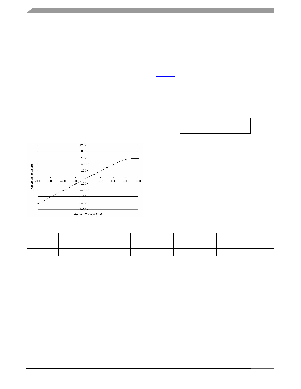
FUNCTIONAL DEVICE OPERATION
LOGIC COMMANDS AND REGISTERS
bit will continue to indicate Logic [1] until the SPI message
following a detection of the zero position, or after the RTZ
feature is commanded OFF using the RTZ message.
• 0 = Return to Zero disabled
• 1 = Return to Zero enabled successfully
[Corrected original entry above to ACC2]
(ACC14:ACC0) Bits OD14:OD0
These 15 bits are from the RTZ accumulator. They
represent the integrated signal present on the non-driven coil
during an RTZ event. These bits are Logic [0] after power-on
reset, or after the
RST pin transitions from Logic [0] to [1].
After an RTZ event, they will represent the last RTZ
accumulator result before the RTZ was stopped.
ACC14 is the MSB and is the sign bit used for zero
detection. Negative numbers have MSB Logic [1] and are
coded in twos complement.
The analog-to-digital converter's linear input range covers
the expected magnitude of motor back e.m.f. signals, which
is usually less than 500mV. Input signals greater than this will
not cause any damage (the circuit is connected to the motor
H-Bridge drivers, and thus is exposed to the full magnitude of
the drive voltages), but may cause some small loss of
linearity. A typical plot of output vs. input is shown in
Figure 13 for 4ms step times.
GAUGE POINTER POSITION STATUS
INFORMATION
Most recent valid PECCR command resulting in the
Gauge Pointer Position status output:
D11
omitted “don’t care--because N/A
D10 D9 D8
1
1 0 0
Figure 13. RTZ Accumulator (Typical)
Table 18. Gauge Pointer Position Status Output Register
Bits
Read
Write
OD15 OD14 OD13 OD12 OD11 OD10 OD9 OD8 OD7 OD6 OD5 OD4 OD3 OD2 OD1 OD0
ENB DIR DIRC CMD POS11 POS10 POS9 POS8 POS7 POS5 POS5 POS4 POS3 POS2 POS1 POS0
– – – – – – – – – – – – – – – –
The bits in Table 18 are read-only bits.
(ENB) Bit OD15
This bit indicates whether the Gauge is enabled.
• 0 = Disabled
• 1 = Enabled
(DIR) Bit OD14
This bit indicates the direction the Gauge is moving.
• 0 = Toward position 0
• 1 = Away from position 0
(DIRC) Bit OD13
This bit is used to determine whether the direction of the
most recent pointer movement is toward the last commanded
position or away from it.
• 0 = Direction of the pointer movement is toward the
commanded position
• 1 = Direction of the pointer movement is away from the
commanded position
(CMD) Bit OD12
This bit indicates whether the gauge is at the most recently
commanded position.
• 0 = At commanded position
• 1 = Not at commanded position
33977
Analog Integrated Circuit Device Data
30 Freescale Semiconductor
Page 31

(POS11:POS0) Bits OD11:OD0
These 12 bits represent the actual position of the pointer
at the time CS transitions to a Logic [0].
GAUGE POINTER VELOCITY STATUS
INFORMATION
Most recent valid PECCR command resulting in the
Gauge and 1 Pointer Velocity status output:
Table 19. Gauge Pointer Velocity STatus Output Register
Bits
Read
Write
OD15 OD14 OD13 OD12 OD11 OD10 OD9 OD8 OD7 OD6 OD5 OD4 OD3 OD2 OD1 OD0
V15 V14 V13 V12 V11 V10 V9 V8 V7 V6 V5 V4 V3 V2 V1 V0
– – – – – – – – – – – – – – – –
D11
x = Don’t Care
D10 D9 D8
1
FUNCTIONAL DEVICE OPERATION
1 1 x
The bits in Table 19 are read-only bits.
(V15:V8) Bits OD15:OD8
These eight bits have no meaning. Velocity position that
identifies it in the un-truncated ramp (e.g., if RS = 2, then the
velocity step location will be 3 when the pointer is at the
commanded position).
(V7:V0) Bits OD7:OD0
These eight bits represent the step table value, [that
deleted PV] indicating the act ua l ve l oc it y st ep l o ca ti on (refer
Table 19) of the Gauge pointer at the time that the CS
to
transitions to a Logic [0].
33977
Analog Integrated Circuit Device Data
Freescale Semiconductor 31
Page 32
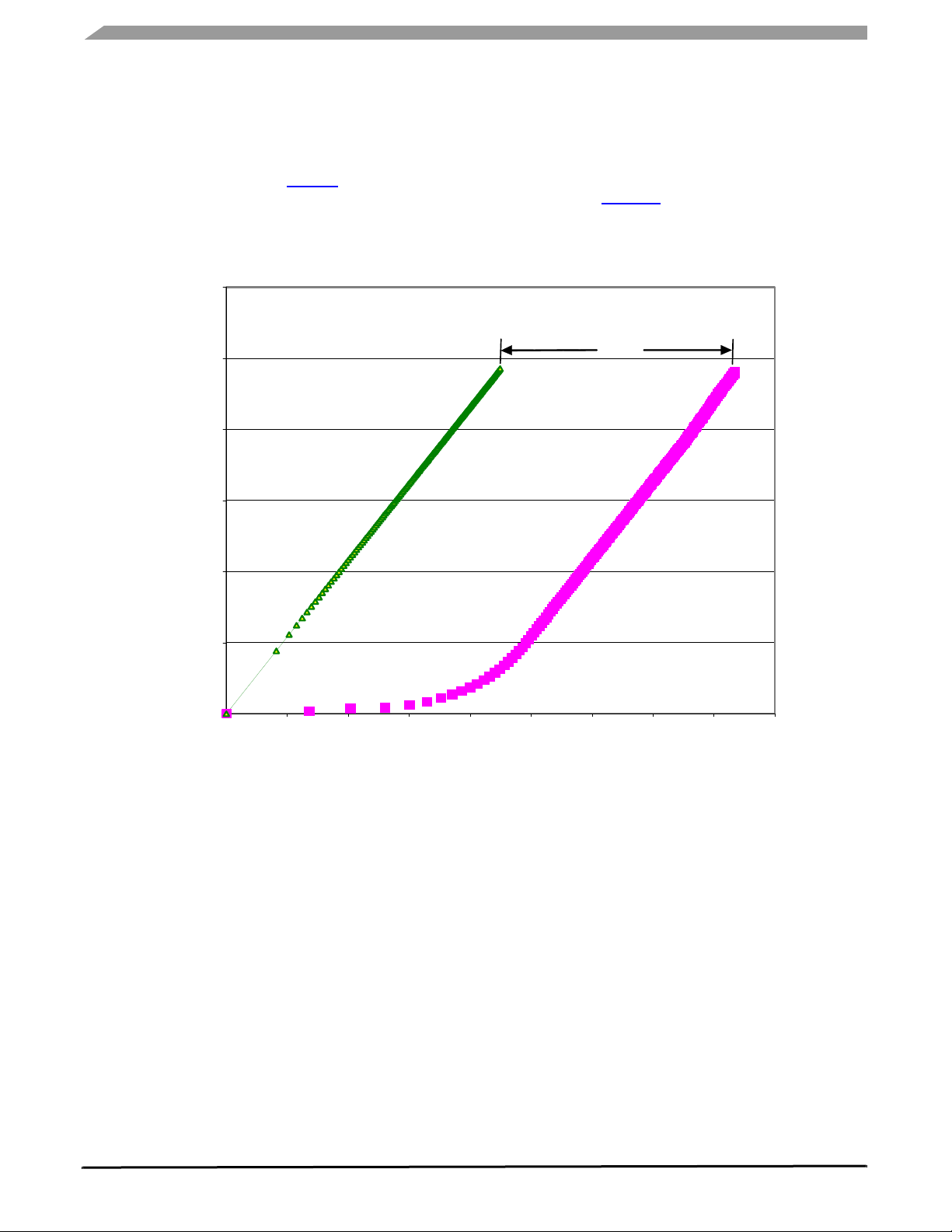
TYPICAL APPLICATIONS
/
TYPICAL APPLICATIONS
The 33977 is an extremely versatile device that can be
used in a variety of applications, Fi gure 1 . The acceleration
and deceleration ramps have been designed for applications
where smooth movement is of the highest prior it y . These
ramps are fixed and the characteristics can be seen in the
6000
5000
4000
S)
3000
SPE E D (usteps
2000
Ide al
Acceleratio n
(4500 deg/s^2)
following figures. For applications where configurable pointer
response and damping are desirable, consider the features
of the MC33976. Figure 14 shows the characteristics of the
acceleration ramp.
76ms
MC33977
Acceleration
1000
0
0 20000 40000 60000 80000 100000 120000 140000 160000 180000
TIME (us)
Figure 14. Acceleration Response Characteristics
33977
Analog Integrated Circuit Device Data
32 Freescale Semiconductor
Page 33
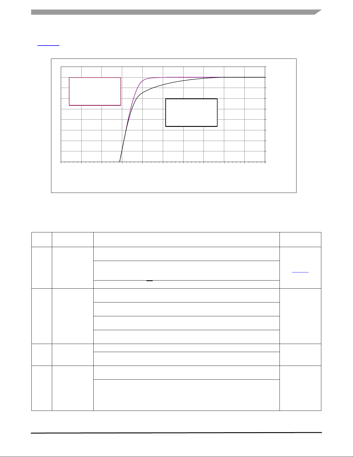
TYPICAL APPLICATIONS
Figure 15 illustrates the deceleration damping characteristics of the device with the hold counts enabled and disabled.
1250
1200
MC33977
without
Hold Counts
MC33977
with
Hold Counts
1150
1100
1050
1000
950
Position (usteps)
900
850
800
0 0.1 0.2 0.3 0.4 0.5 0.6 0.7 0.8 0.9 1
Time (s)
Figure 15. Deceleration Damping Response Examples
Table 20 provides a step-by-step example of configuring
and using many of the features designed into the IC This
example is intended to familiarize users with some of the
device features.
Table 20. 33977 Setup, Configuration, and Usage Example
Step Command Description
a) Enables the gauge
• Bit PE0: Gauge enable bit
1
2 RTZCR
4 POSR
5 PECCR
PECCR
b) Clock calibration
• Bit PE3: Enables calibration procedure
• Bit PE4: Set clock f = 1.0 MHz maximum or nominal
c) Send 8.0 µs pulse on CS to calibrate 1.0 MHz clock
a) Set RTZ full step time
• Bit RC3:RC0
b) Set RTZ blanking time
• Bits RC4
c) Preload RTZ accumulator
• Bits RC12:RC11 and RC10:RC5
d) Check SO for an out-of-range clock calibration
• Is Bit CAL Logic [1}? If so, repeat Steps 1 and 2
a) Move pointer to position 12 prior to RTZ
b) Check SO to determine if gauge has moved
• Is bit MOV (OD4) Logic [1]? If so, the gauge moved to the first microstep
a) Send null command to determine if gauges moved
• Bit PE12
b) Check SO to determine if the gauge has moved
• Is bit MOV (OD4) Logic [1]? If so, the gauge moved another microstep since the last
SPI message. Keep track of movement and if 12 steps are finished, and both gauges
are at a static position, the RTZ. Otherwise, repeat steps a) and b).
• Bit CMD (OD10) could also be monitored to determine if the pointer is static.
Reference Table
and/or Figure
Table 9,
Figure 8
Table 13
Table 14
Table 15
Table 9
Table 16
Table 11
Table 9
Table 16
Table 9
Table 9
Table 16
33977
Analog Integrated Circuit Device Data
Freescale Semiconductor 33
Page 34

TYPICAL APPLICATIONS
Table 20. 33977 Setup, Configuration, and Usage Example
Step Command Description
a) Return the gauge to the zero stop using the RTZ command
• Bit RZ1 enables or disables an RTZ
6 RTZ
7 PECCR
10 VELR
11 POSR
13 POSR
15
16
17
20
PECCR
RTZ
PECCR
PECCR
• Bits RZ2 and PE7 select the direction
These will be used if characterizing the RTZ.
a) Check the status of the RTZ by sending the null command to monitor bit RTZ of the
Device Status SO.
• Bit PE12 is the null command
b) Is RTZ (OD2) Logic [1]? If not, the gauge is still returning and null command should be
resent.
a) Change the maximum velocity of the gauge
• Bit V8 enables a change to the maximum velocity
• Bits V7:V10 determine the maximum velocity position from Table 6, Velocity Table
a) Position gauge pointer
• Bits P011:P00: Desired pointer position
b) Check SO for out-of-range V
PWR
• Is bit OVUV (OD6) Logic [1] If so, use UV (OD8) and OV (OD9) to decide whether to
RTZ after valid V
PWR
c) Check SO for overtemperature
• Is bit OT Logic [1]? If so, enable driver again. If OT continues to indicate
overtemperature, shut down the gauge.
• Once OT returns to normal, re-establish the zero reference by RTZ command.
a) Return the pointer close to zero position using POSR
b) Move pointer position at least 12 microsteps CW to the nearest full step prior to RTZ
f) Send null command to see if gauges moved
• Bit PE12
g) Check SO to determine if the gauge moved.
• Is bit MOV (OD4) Logic [1]? If so, the gauge moved another microstep since the last
SPI message. Keep track of movement and if 12 steps are finished, and both gauges
are at a static position, then RTZ. Otherwise, repeat steps a) and b).
• Bit CMD (OD10) could also be monitored to determine the pointer is static.
a) Return the gauge to the zero stop using the RTZ command.
• Bit RZ1 enables or disables an RTZ
• Bits RZ2 and PE7 select the direction
b) Select the RTZ accumulator bits clocking out on the SO bits using bits PE11:PE10
These will be used if characterizing the RTZ.
a) Check the status of the RTZ by sending the null command to monitor SO bit RTZ
• Bit PE12 is the null command
b) Is RTZ Logic [0]? If not, the gauge is still returning and null command should be resent
a) Disable the gauge driver and go to standby
• Bit PE0:PE1 disable the gauge
b) Put the device to sleep
• RST pin is pulled to Logic [0]
Reference Table
and/or Figure
Table 12
Table 9
Table 15b) Select the RTZ accumulator bits to clock out on the SO bits using bits PE11:PE10.
Table 9
Table 16
Table 9
Table 6
Table 11
Table 6
Table 11
Table 9
Table 16
TABLE 9
TABLE 12
TABLE 16
TABLE 9
TABLE 16
TABLE 9
33977
Analog Integrated Circuit Device Data
34 Freescale Semiconductor
Page 35
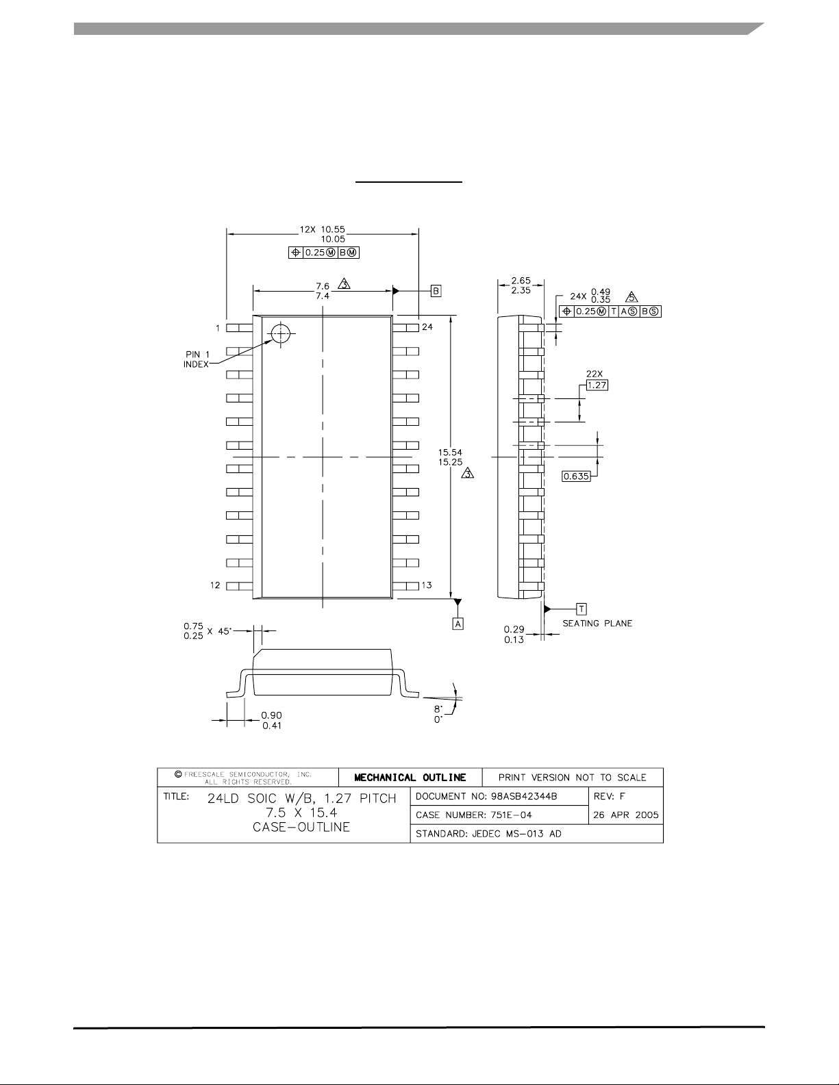
PACKAGE DIMENSIONS
PACKAGING
PACKAGING
PACKAGE DIMENSIONS
For the most current revision of the package, visit www.freescale.com and do a keyword search using the “98A” number listed
below.
DW SUFFIX
EG SUFFIX (PB-FREE)
24-PIN
PLASTIC PACKAGE
98ASB42344B
ISSUE F
33977
Analog Integrated Circuit Device Data
Freescale Semiconductor 35
Page 36

REVISION HISTORY
REVISION HISTORY
REVISION DATE DESCRIPTION OF CHANGES
1.0
2.0
8/2006
1/2007
• Initial release
• Updated to the current Freescale format
• Revised Internal Block Diagram to enhance readability
• Added parameter Peak Package Reflow Temperature During Reflow
and notes
(4)
and
(5)
• Made wording additions to Address 101 - Gauge Return to Zero Configuration Register
on page 25 and (RC12:RC11) Bits D12:D11 on pa ge 26
• Added ADC Gain
(12), (14)
• Added RTZ Accumulator (Typical) on page 30 and accompanying text
to Static Electrical Characteristics table
(4), (5)
on page 4
33977
Analog Integrated Circuit Device Data
36 Freescale Semiconductor
Page 37

How to Reach Us:
Home Page:
www.freescale.com
Web Support:
http://www.freescale.com/support
USA/Europe or Locations Not Listed:
Freescale Semiconductor, Inc.
Technical Information Center, EL516
2100 East Elliot Road
Tempe, Arizona 85284
+1-800-521-6274 or +1-480-768-2130
www.freescale.com/support
Europe, Middle East, and Africa:
Freescale Halbleiter Deutschland GmbH
Technical Information Center
Schatzbogen 7
81829 Muenchen, Germany
+44 1296 380 456 (English)
+46 8 52200080 (English)
+49 89 92103 559 (German)
+33 1 69 35 48 48 (French)
www.freescale.com/support
Japan:
Freescale Semiconductor Japan Ltd.
Headquarters
ARCO Tower 15F
1-8-1, Shimo-Meguro, Meguro-ku,
Tokyo 153-0064
Japan
0120 191014 or +81 3 5437 9125
[email protected]
Asia/Pacific:
Freescale Semiconductor Hong Kong Ltd.
Technical Information Center
2 Dai King Street
Ta i Po Industrial Estate
Tai Po, N.T., Hong Kong
+800 2666 8080
[email protected]
For Literature Requests Only:
Freescale Semiconductor Literature Distribution Center
P.O. Box 5405
Denver, Colorado 80217
1-800-441-2447 or 303-675-2140
Fax: 303-675-2150
[email protected]
RoHS-compliant and/or Pb-free versions of Freescale products have the functionality
and electrical characteristics of their non-RoHS-compliant and/or non-Pb- free
counterparts. For further information, see http://www.freescale.com or contact your
Freescale sales representative.
For information on Freescale’s Environmental Products program, go to http://
www.freescale.com/epp.
Information in this document is provided solely to enable system and software
implementers to use Freescale Semiconductor products. There are no express or
implied copyright licenses granted hereunder to design or fabricate any integrated
circuits or integrated circuits base d on the information in this document.
Freescale Semiconductor reserves the right to make changes without further notice to
any products herein. Freescale Semiconductor makes no warranty, representation or
guarantee regarding the suitability of its products for any particular purpose, nor does
Freescale Semiconductor assume any liability arising out of the application o r use of any
product or circuit, and specifically disclaims any and all liability, including without
limitation consequential or incidental damages. “Typical” parameters that may be
provided in Freescale Semiconductor data sheet s and/or specifications can and do vary
in different applications and actual performance may vary over time. All operating
parameters, including “Typicals”, must be validated for each customer application by
customer’s technical experts. Freescale Semiconductor does not convey any license
under its patent rights nor the rights of others. Freescale Semiconductor products are
not designed, intended, or authorized for use as components in systems intended for
surgical implant into the body, or other applications intended to support or sustain life,
or for any other application in which the failure of the Freescale Semiconduct or product
could create a situation where personal injury or death may occur. Should Buyer
purchase or use Freescale Semiconductor products for any such unintended or
unauthorized application, Buyer shall indemnify and hold Freescale Semiconductor and
its officers, employees, subsidiaries, affiliates, and distributors harmless against all
claims, costs, damages, and expenses, and reasonable attorney fee s arising out of,
directly or indirectly, any claim of personal injury or death associated with such
unintended or unauthorized use, even if such claim alleges that Freescale
Semiconductor was negligent regarding the design or manufacture of the part.
Freescale™ and the Freescale logo are trademarks of Freescale Semiconductor, Inc.
All other product or service names are the property of their respective owners.
© Freescale Semiconductor, Inc., 2007. All rights reserved.
MC33977
Rev. 2.0
1/2007
 Loading...