

Page 1
2SC4791
Silicon NPN Epitaxial
Application
VHF / UHF wide band amplifier
Features
• High gain bandwidth product
fT = 10 GHz Typ.
• High gain, low noise figure
PG = 15.5 dB Typ, NF = 1.2 dB Typ at f = 900 MHz
Outline
MPAK-4
2
3
1
4
1. Collector
2. Emitter
3. Base
4. Emitter
Page 2

2SC4791
Absolute Maximum Ratings (Ta = 25°C)
Item Symbol Ratings Unit
Collector to base voltage V
Collector to emitter voltage V
Emitter to base voltage V
Collector current I
Collector power dissipation P
CBO
CEO
EBO
C
C
Junction temperature Tj 150 °C
Storage temperature Tstg –55 to +150 °C
Electrical Characteristics (Ta = 25°C)
Item Symbol Min Typ Max Unit Test conditions
Collector cutoff current I
Emitter cutoff current I
DC current transfer ratio h
CBO
I
CEO
EBO
FE
Collector output capacitance Cob — 0.4 0.75 pF VCB = 5 V, IE = 0, f = 1 MHz
Gain bandwidth product f
T
Power gain PG 12.5 15.5 — dB VCE = 5 V, IC = 10 mA,
Noise figure NF — 1.2 2.5 dB VCE = 5 V, IC = 5 mA,
Note: Marking is “YA–”.
——10µAVCB = 15 V, IE = 0
——1 mAV
——10µAVEB = 1.5 V, IC = 0
50 120 250 VCE = 5 V, IC = 10 mA
7.0 10.0 — GHz VCE = 5 V, IC = 10 mA
15 V
8V
1.5 V
20 mA
150 mW
= 8 V, RBE = ∞
CE
f = 900 MHz
f = 900 MHz
Attention: This is electrostatic sensitive device.
2
Page 3
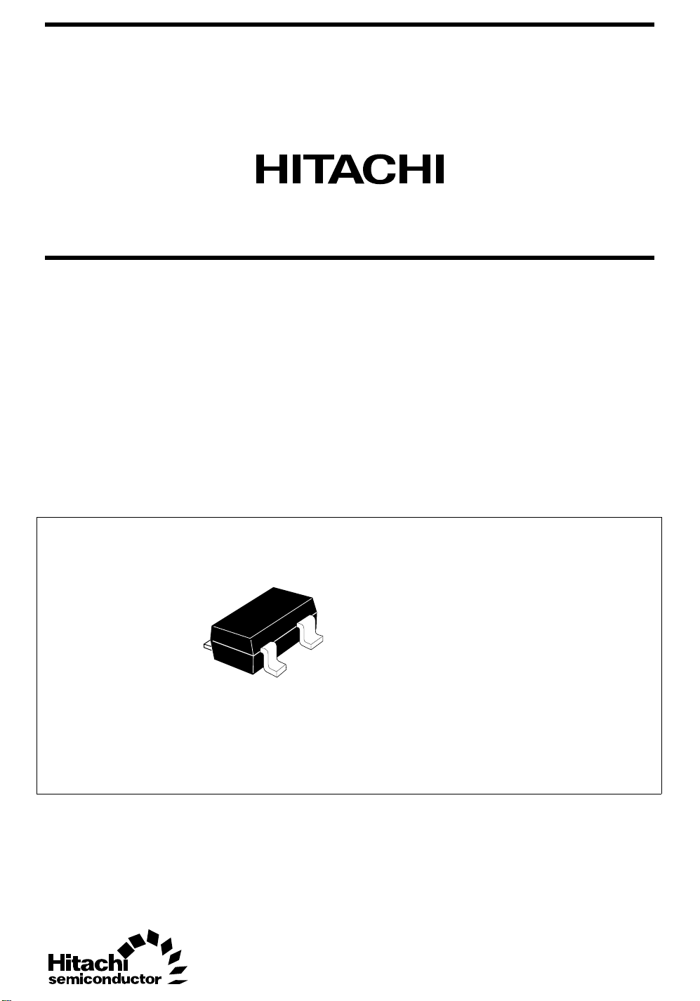
Maximum Collector Dissipation Curve
150
(mW)
C
100
200
FE
160
120
DC Current Transfer Ratio
vs. Collector Current
V = 5V
CE
2SC4791
50
Collector Power Dissipation P
0
Ambient Temperature Ta (°C)
15010050
Gain Bandwidth Product
vs. Collector Current
12
V = 5 V
CE
10
T
8
6
V = 1 V
CE
4
2
Gain Bandwidth Product f (GHz)
0
12 51020 50
Collector Current I (mA)
C
80
V = 1V
CE
40
DC Current Transfer Ratio h
0
0.1
0.2 0.5 1 2 5 10 20 50
Collector Current I (mA)
C
Collector Output Capacitance vs.
Collector to Base Voltage
0.56
I = 0
E
0.52
f = 1 MHz
0.48
0.44
0.40
0.36
Collector Output Capacitance Cob (pF)
0.5
12 51020
Collector to Base Voltage V (V)
CB
3
Page 4
2SC4791
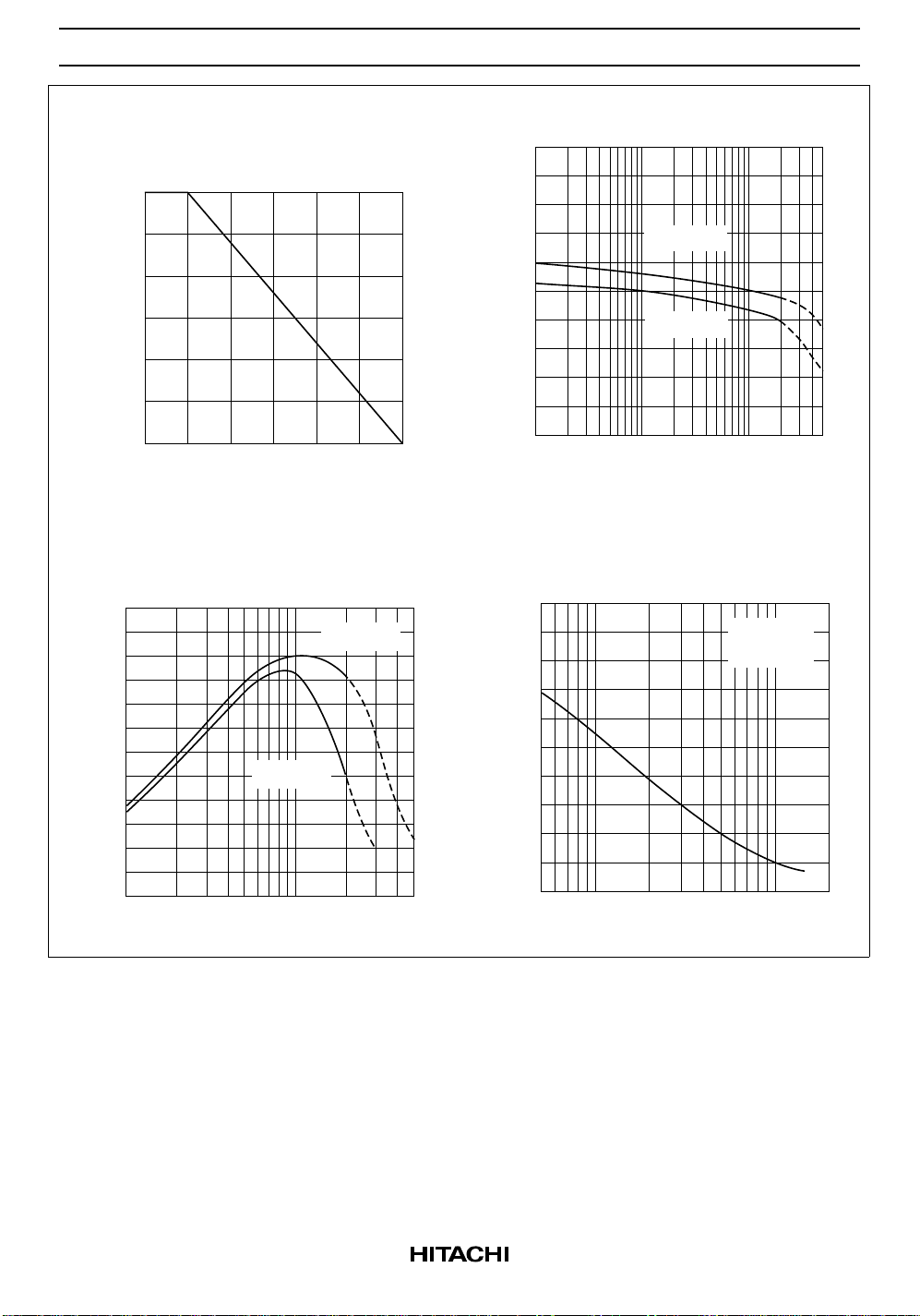
Power Gain vs. Collector Current
20
f = 900 MHz
16
12
8
Power Gain PG (dB)
4
0
0.3
1310
Collector Current I (mA)
V = 5V
CE
V = 1V
CE
C
30
Noise Figure vs. Collector Current
5
f = 900 MHz
4
3
2
Noise Figure NF (dB)
1
V = 5V
CE
V = 1V
CE
0
0.3 1 3 10 30
Collector Current I (mA)
C
4
Page 5

2SC4791
S11 Parameter vs. Frequency
1
.8
.6
.4
.2
.4
0
.2
.6 .8
1.0
1.5
–.2
–.4
–.6
–.8
–1
Condition: V = 5 V , Zo = 50
CE
200 to 2000 MHz (200 MHz step)
(I = 5 mA)
C
(I = 10 mA)
C
S12 Parameter vs. Frequency
1.5
2
–1.5
2
345
–2
Ω
3
10
–3
4
–4
5
–10
–5
10
180°
–150°
S21 Parameter vs. Frequency
90°
120°
150°
–120°
Condition: V = 5 V , Zo = 50
–90°
CE
200 to 2000 MHz (200 MHz step)
(I = 5 mA)
C
(I = 10 mA)
C
S22 Parameter vs. Frequency
Scale: 4 / div.
60°
30°
0°
–30°
–60°
Ω
180°
–150°
120°
90°
150°
–120°
Condition: V = 5 V , Zo = 50
–90°
CE
200 to 2000 MHz (200 MHz step)
(I = 5 mA)
C
(I = 10 mA)
C
Scale: 0.04 / div.
60°
30°
0°
–30°
–60°
Ω
1
.8
.6
.4
.2
.4 .6
.8 1.0 2 3 4 5 10
0
.2
1.5
–.2
–.4
–.6
–.8
–1
Condition: V = 5 V , Zo = 50
CE
200 to 2000 MHz (200 MHz step)
(I = 5 mA)
C
(I = 10 mA)
C
1.5
–1.5
2
–2
3
4
5
10
–10
–5
–4
–3
Ω
5
Page 6

2SC4791
S11 Parameter vs. Frequency
1
.8
.6
.4
.2
0
.2 .4
.6 .8
1.0
1.5
–.2
–.4
–.6
–.8
Condition: V = 1 V , Zo = 50
CE
–1
–1.5
200 to 2000 MHz (200 MHz step)
(I = 0.5 mA)
C
(I = 1 mA)
C
S12 Parameter vs. Frequency
1.5
2
S21 Parameter vs. Frequency
Scale: 0.8 / div.
2
120°
3
4
5
150°
90°
60°
30°
10
10
5
4
3
180°
0°
–10
–5
–3
–4
–150°
–30°
–2
–120°
Ω
Condition: V = 1 V , Zo = 50
–90°
CE
–60°
Ω
200 to 2000 MHz (200 MHz step)
(I = 0.5 mA)
C
(I = 1 mA)
C
S22 Parameter vs. Frequency
180°
–150°
150°
Scale: 0.06 / div.
90°
120°
–120°
Condition: V = 1 V , Zo = 50
–90°
CE
60°
–60°
200 to 2000 MHz (200 MHz step)
(I = 0.5 mA)
C
(I = 1 mA)
C
30°
–30°
Ω
0°
1
.8
.6
.4
.2
0
.2
.4
.6 .8 1.0
1.5
–.2
–.4
–.6
–.8
–1
Condition: V = 1 V , Zo = 50
CE
200 to 2000 MHz (200 MHz step)
(I = 0.5 mA)
C
(I = 1 mA)
C
1.5
2
–1.5
2
3
345 10
–3
–2
Ω
4
–4
5
10
–10
–5
6
Page 7

2SC4791
S Parameter (VCE = 5 V, IC = 5 mA, ZO = 50 Ω, Emitter Common)
Freq. S11 S21 S12 S22
(MHz) MAG. ANG. MAG. ANG. MAG. ANG. MAG. ANG.
100 0.859 –15.9 13.192 165.5 0.016 82.3 0.974 –9.3
200 0.790 –30.6 12.225 151.9 0.031 73.9 0.914 –17.5
300 0.700 –44.0 10.967 139.9 0.043 68.2 0.841 –24.2
400 0.618 –54.8 9.802 130.2 0.053 64.0 0.771 –29.2
500 0.543 –64.7 8.686 122.4 0.061 61.4 0.710 –32.5
600 0.477 –73.3 7.761 116.0 0.068 59.8 0.660 –34.8
700 0.421 –80.1 6.955 110.2 0.074 58.9 0.619 –36.7
800 0.369 –86.3 6.316 105.5 0.080 58.7 0.584 –38.2
900 0.331 –92.8 5.748 101.0 0.086 58.1 0.557 –39.3
1000 0.287 –99.4 5.275 97.6 0.091 57.9 0.535 –40.3
1100 0.226 –104.8 4.869 94.1 0.097 57.9 0.517 –41.2
1200 0.220 –110.7 4.498 90.6 0.102 58.1 0.502 –42.1
1300 0.200 –110.7 4.169 88.2 0.107 58.4 0.492 –43.1
1400 0.179 –125.0 3.926 85.4 0.113 58.2 0.479 –44.2
1500 0.159 –131.7 3.698 83.0 0.119 58.2 0.471 –44.9
1600 0.142 –138.0 3.493 80.5 0.125 58.4 0.463 –46.0
1700 0.126 –147.6 3.311 78.1 0.130 58.5 0.456 –47.2
1800 0.117 –154.1 3.143 76.1 0.136 58.2 0.450 –48.2
1900 0.109 –166.9 3.008 74.0 0.142 58.0 0.445 –49.3
2000 0.102 179.8 2.864 71.9 0.147 57.9 0.440 –50.4
7
Page 8

2SC4791
S Parameter (VCE = 5 V, IC = 10 mA, ZO = 50 Ω, Emitter Common)
Freq. S11 S21 S12 S22
(MHz) MAG. ANG. MAG. ANG. MAG. ANG. MAG. ANG.
100 0.758 –22.4 19.871 159.8 0.015 78.6 0.942 –12.6
200 0.650 –41.5 17.252 142.4 0.028 71.0 0.842 –22.5
300 0.538 –57.1 14.423 129.0 0.037 66.8 0.739 –28.5
400 0.445 –69.1 12.168 119.4 0.045 64.3 0.659 –32.0
500 0.383 –79.6 10.376 112.2 0.052 63.3 0.600 –33.7
600 0.320 –87.8 8.995 106.7 0.058 63.4 0.577 –34.9
700 0.274 –95.4 7.914 101.8 0.065 63.7 0.524 –35.4
800 0.230 –102.4 7.057 97.8 0.071 64.0 0.499 –36.3
900 0.205 –109.8 6.332 93.9 0.076 64.4 0.480 –36.7
1000 0.174 –116.9 5.778 91.0 0.083 64.5 0.466 –37.4
1100 0.154 –125.9 5.291 88.1 0.089 64.6 0.454 –38.0
1200 0.131 –135.1 4.862 85.4 0.096 64.7 0.444 –38.7
1300 0.118 –142.7 4.508 82.9 0.102 64.6 0.438 –39.4
1400 0.108 –154.7 4.226 80.8 0.109 64.5 0.431 –40.4
1500 0.104 –165.2 3.961 78.7 0.116 64.3 0.426 –41.4
1600 0.093 –178.6 3.718 76.4 0.122 64.1 0.420 –42.4
1700 0.095 169.4 3.532 74.3 0.129 64.0 0.417 –43.6
1800 0.094 158.4 3.347 72.4 0.135 63.4 0.413 –44.8
1900 0.094 148.2 3.190 70.5 0.142 63.2 0.409 –46.0
2000 0.101 136.0 3.036 68.6 0.148 63.0 0.406 –47.3
8
Page 9

2SC4791
S Parameter (VCE = 1 V, IC = 0.5 mA, ZO = 50 Ω, Emitter Common)
Freq. S11 S21 S12 S22
(MHz) MAG. ANG. MAG. ANG. MAG. ANG. MAG. ANG.
100 0.983 –6.6 1.757 174.0 0.023 85.8 0.995 –4.1
200 0.976 –13.1 1.723 167.3 0.047 80.7 0.990 –8.2
300 0.961 –19.6 1.741 160.2 0.071 76.4 0.980 –12.3
400 0.938 –26.2 1.734 154.0 0.093 71.9 0.966 –16.4
500 0.920 –32.5 1.666 147.6 0.093 67.6 0.950 –20.1
600 0.903 –38.6 1.629 142.6 0.133 63.4 0.932 –23.9
700 0.868 –44.6 1.584 136.2 0.151 59.9 0.913 –27.3
800 0.836 –50.4 1.564 130.6 0.166 56.2 0.891 –30.6
900 0.819 –56.1 1.520 125.3 0.180 52.8 0.869 –33.8
1000 0.780 –61.6 1.484 120.3 0.193 49.5 0.849 –36.8
1100 0.749 –66.9 1.434 115.3 0.204 46.7 0.828 –39.6
1200 0.713 –71.7 1.369 110.4 0.213 44.0 0.810 –42.1
1300 0.687 –77.0 1.322 107.2 0.221 41.4 0.794 –44.8
1400 0.659 –82.2 1.317 102.3 0.229 38.9 0.774 –47.3
1500 0.629 –86.9 1.282 98.5 0.234 36.7 0.757 –49.7
1600 0.601 –91.2 1.248 94.6 0.239 34.6 0.741 –51.9
1700 0.578 –96.7 1.215 91.0 0.243 32.4 0.726 –54.2
1800 0.656 –101.0 1.187 87.5 0.248 30.4 0.713 –56.3
1900 0.532 –106.3 1.155 84.4 0.249 28.9 0.699 –58.4
2000 0.508 –111.4 1.124 81.0 0.251 27.3 0.686 –60.5
9
Page 10

2SC4791
S Parameter (VCE = 1 V, IC = 1 mA, ZO = 50 Ω, Emitter Common)
Freq. S11 S21 S12 S22
(MHz) MAG. ANG. MAG. ANG. MAG. ANG. MAG. ANG.
100 0.969 –8.3 3.406 172.8 0.023 84.7 0.992 –5.3
200 0.953 –16.4 3.337 165.1 0.046 79.1 0.980 –10.3
300 0.927 –25.1 3.270 157.0 0.070 73.7 0.960 –15.8
400 0.896 –33.0 3.218 149.3 0.090 68.8 0.933 –20.8
500 0.860 –40.5 3.068 143.0 0.108 64.2 0.905 –25.1
600 0.820 –47.7 2.950 136.9 0.124 59.7 0.874 –29.3
700 0.778 –54.5 2.816 130.7 0.139 56.3 0.844 –33.2
800 0.731 –61.1 2.711 124.8 0.151 52.9 0.810 –36.7
900 0.703 –67.5 2.580 119.7 0.162 49.8 0.780 –39.9
1000 0.657 –73.8 2.470 114.8 0.171 46.9 0.752 –42.8
1100 0.617 –79.8 2.363 110.2 0.178 44.7 0.725 –45.5
1200 0.575 –84.8 2.229 105.3 0.185 42.5 0.703 –47.7
1300 0.549 –89.8 2.104 102.4 0.191 40.8 0.686 –50.1
1400 0.516 –96.2 2.053 97.9 0.196 38.8 0.660 –52.5
1500 0.485 –101.5 1.975 94.3 0.199 37.6 0.641 –54.5
1600 0.456 –106.7 1.891 90.9 0.203 36.2 0.623 –56.4
1700 0.429 –111.9 1.827 87.8 0.206 34.9 0.607 –58.3
1800 0.412 –115.9 1.751 84.6 0.209 33.7 0.593 –60.3
1900 0.389 –122.6 1.700 81.7 0.211 33.2 0.580 –62.1
2000 0.368 –128.0 1.645 78.8 0.212 32.4 0.567 –64.1
10
Page 11

0.4
+ 0.1
– 0.05
2.95 ± 0.2
1.9 ± 0.2
0.95 0.95
0.4
+ 0.1
– 0.05
0.65
0.16
+ 0.1
– 0.06
Unit: mm
0.4
+ 0.1
– 0.05
0.95
1.8 ± 0.2
0.85
0.6
+ 0.1
– 0.05
0.3
+ 0.2
1.1
1.5 ± 0.15
0.65
– 0.1
+ 0.2
– 0.6
2.8
Hitachi Code
JEDEC
EIAJ
Weight
0 – 0.1
(reference value)
MPAK-4
—
Conforms
0.013 g
Page 12

Cautions
1. Hitachi neither warrants nor grants licenses of any rights of Hitachi’s or any third party’s patent,
copyright, trademark, or other intellectual property rights for information contained in this document.
Hitachi bears no responsibility for problems that may arise with third party’s rights, including
intellectual property rights, in connection with use of the information contained in this document.
2. Products and product specifications may be subject to change without notice. Confirm that you have
received the latest product standards or specifications before final design, purchase or use.
3. Hitachi makes every attempt to ensure that its products are of high quality and reliability. However,
contact Hitachi’s sales office before using the product in an application that demands especially high
quality and reliability or where its failure or malfunction may directly threaten human life or cause risk
of bodily injury, such as aerospace, aeronautics, nuclear power, combustion control, transportation,
traffic, safety equipment or medical equipment for life support.
4. Design your application so that the product is used within the ranges guaranteed by Hitachi particularly
for maximum rating, operating supply voltage range, heat radiation characteristics, installation
conditions and other characteristics. Hitachi bears no responsibility for failure or damage when used
beyond the guaranteed ranges. Even within the guaranteed ranges, consider normally foreseeable
failure rates or failure modes in semiconductor devices and employ systemic measures such as failsafes, so that the equipment incorporating Hitachi product does not cause bodily injury, fire or other
consequential damage due to operation of the Hitachi product.
5. This product is not designed to be radiation resistant.
6. No one is permitted to reproduce or duplicate, in any form, the whole or part of this document without
written approval from Hitachi.
7. Contact Hitachi’s sales office for any questions regarding this document or Hitachi semiconductor
products.
Hitachi, Ltd.
Semiconductor & Integrated Circuits.
Nippon Bldg., 2-6-2, Ohte-machi, Chiyoda-ku, Tokyo 100-0004, Japan
Tel: Tokyo (03) 3270-2111 Fax: (03) 3270-5109
URL NorthAmerica : http:semiconductor.hitachi.com/
For further information write to:
Hitachi Semiconductor
(America) Inc.
179 East Tasman Drive,
San Jose,CA 95134
Tel: <1> (408) 433-1990
Fax: <1>(408) 433-0223
Europe : http://www.hitachi-eu.com/hel/ecg
Asia (Singapore) : http://www.has.hitachi.com.sg/grp3/sicd/index.htm
Asia (Taiwan) : http://www.hitachi.com.tw/E/Product/SICD_Frame.htm
Asia (HongKong) : http://www.hitachi.com.hk/eng/bo/grp3/index.htm
Japan : http://www.hitachi.co.jp/Sicd/indx.htm
Hitachi Europe GmbH
Electronic components Group
Dornacher Stra§e 3
D-85622 Feldkirchen, Munich
Germany
Tel: <49> (89) 9 9180-0
Fax: <49> (89) 9 29 30 00
Hitachi Europe Ltd.
Electronic Components Group.
Whitebrook Park
Lower Cookham Road
Maidenhead
Berkshire SL6 8YA, United Kingdom
Tel: <44> (1628) 585000
Fax: <44> (1628) 778322
Hitachi Asia Pte. Ltd.
16 Collyer Quay #20-00
Hitachi Tower
Singapore 049318
Tel: 535-2100
Fax: 535-1533
Hitachi Asia Ltd.
Taipei Branch Office
3F, Hung Kuo Building. No.167,
Tun-Hwa North Road, Taipei (105)
Tel: <886> (2) 2718-3666
Fax: <886> (2) 2718-8180
Copyright ' Hitachi, Ltd., 1999. All rights reserved. Printed in Japan.
Hitachi Asia (Hong Kong) Ltd.
Group III (Electronic Components)
7/F., North Tower, World Finance Centre,
Harbour City, Canton Road, Tsim Sha Tsui,
Kowloon, Hong Kong
Tel: <852> (2) 735 9218
Fax: <852> (2) 730 0281
Telex: 40815 HITEC HX
 Loading...