

Page 1
2SC4197
Silicon NPN Epitaxial
Application
UHF frequency converter, wide band amplifier
Outline
MPAK
3
1
2
1. Emitter
2. Base
3. Collector
Page 2
2SC4197
Absolute Maximum Ratings (Ta = 25°C)
Item Symbol Ratings Unit
Collector to base voltage V
Collector to emitter voltage V
Emitter to base voltage V
Collector current I
Collector power dissipation P
CBO
CEO
EBO
C
C
Junction temperature Tj 150 °C
Storage temperature Tstg –55 to +150 °C
Electrical Characteristics (Ta = 25°C)
Item Symbol Min Typ Max Unit Test conditions
Collector to base breakdown
V
(BR)CBO
voltage
Collector cutoff current I
Collector cutoff current I
Emitter cutoff current I
Collector to emitter saturation
V
CBO
CEO
EBO
CE(sat)
voltage
DC current transfer ratio h
FE
Collector output capacitance Cob — 0.85 1.3 pF VCB = 10 V, IE = 0, f = 1MHz
Gain bandwidth product f
T
Conversion gain CG — 19 — dB VCC = 5 V, IC = 0.8 mA,
Noise figure NF — 8 — dB f
Note: Marking is “TI–”.
25——V I
— — 0.1 µAVCB = 15 V, IE = 0
——10µAVCE = 13 V, RBE = ∞
— — 0.3 µAVEB = 3 V, IC = 0
— — 0.3 V IC = 20 mA, IB = 4 mA
50 — 180 VCE = 5 V, IC = 5 mA
3.0 3.8 — GHz VCE = 5 V, IC = 20 mA
25 V
13 V
3V
50 mA
150 mW
= 10 µA, IE = 0
C
f
= 900 MHz
in
= 930 MHz (–5dBm),
osc
f
= 30 MHz
out
2
Page 3
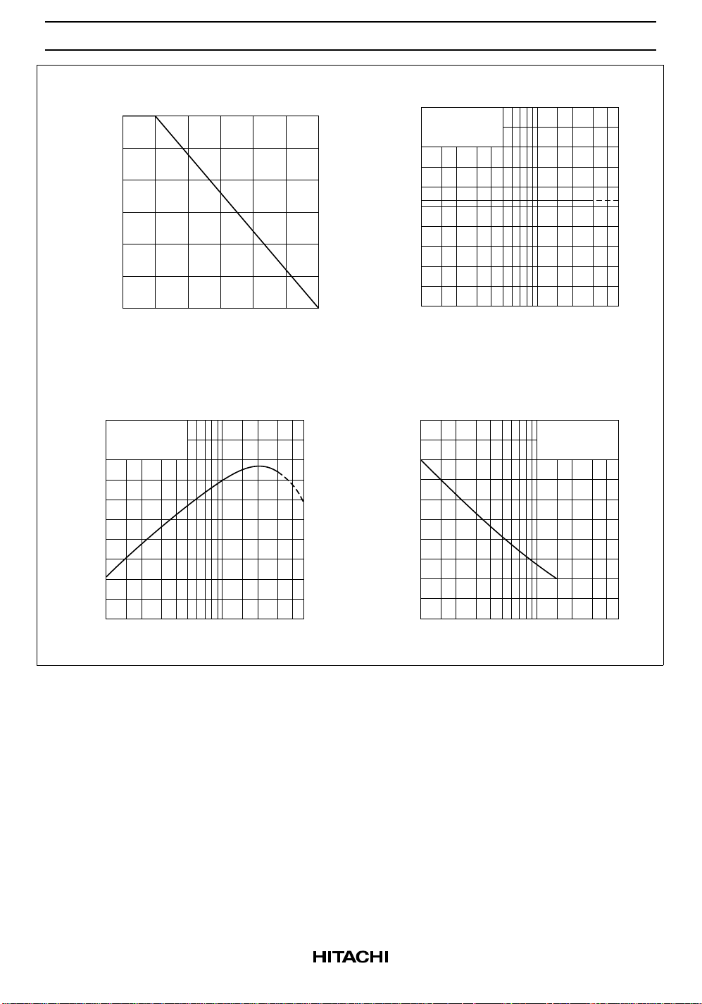
Maximum Collector Dissipation Curve
150
(mW)
C
FE
2SC4197
DC Current Transfer Ratio vs.
Collector Current
200
VCE = 5 V
160
100
50
Collector Power Dissipation P
0
15010050
Ambient Temperature Ta (°C)
Gain Bandwidth Product vs.
Collector Current
5
VCE = 5 V
4
(GHz)
T
3
2
1
Gain Bandwidth Product f
0
152021050
Collector Current I
(mA)
C
120
80
40
DC Current Transfer Ratio h
0
152021050
Collector Current I
(mA)
C
Collector Output Capacitance vs.
Collector to Base Voltage
1.2
IE = 0
(pF)
ob
1.1
f = 1 MHz
1.0
0.9
0.8
Collector Output Capacitance C
0.7
152021050
Collector to Base Voltage V
CB
(V)
3
Page 4

2SC4197
Conversion Gain, Noise Figure
vs. Supply Voltage
25
I
= 0.8 mA
C
f = 900 MHz
20
CG
15
10
NF
Noise Figure NF (dB)
5
Conversion Gain CG (dB)
f
= 30 MHz
out
= 930 MHz (–5 dBm)
f
osc
0
15210
Supply Voltage V
CC
(V)
Conversion Gain, Noise Figure
vs. Collector Current
25
VCC = 5 V
f = 900 MHz
20
Conversion Gain, Noise Figure
vs. Collector Current
25
VCC = 3 V
f = 900 MHz
20
15
10
Noise Figure NF (dB)
5
Conversion Gain CG (dB)
0
f
= 30 MHz
out
f
= 930 MHz (–5 dBm)
osc
0.1 0.5 20.2 1.0 5
Collector Current I
C
CG
CG
NF
(mA)
15
10
Noise Figure NF (dB)
5
Conversion Gain CG (dB)
0
f
= 30 MHz
out
f
= 930 MHz (–5 dBm)
osc
0.1 0.5 20.2 1.0 5
Collector Current I
C
NF
(mA)
4
Page 5

S Parameters (Emitter Common)
Test Condition VCE = 5 V, 100 MHz to 1000 MHz (100 MHz Step), ZO = 50 Ω
IC = 5 mA
I
= 10 mA
C
2SC4197
0.2
0
–0.2
0.4
–0.4
150°
0.6
0.2 0.4
–0.6
–0.8
120°
S11-Frequency
1
0.8
0.6
0.8
1 1.5 2 3 45 10
–1
S12-Frequency
1.5
–1.5
–2
2
Scale : 0.04/div90°
60°
3
–3
4
–4
5
–5
10
∞
–10
30°
–180°
0.2
150°
–150°
0.4
120°
–120°
0.6
S21-Frequency
90°
–90°
S22-Frequency
1
0.8
Scale : 4/div
60°
30°
0°
–30°
–60°
1.5
2
3
4
5
–180°
–150°
–120°
–90°
–60°
–30°
10
0.6
0.8
1 1.5 2 3 45 10
–2
–1
–1.5
∞
–10
–5
–4
–3
–0.4
0.2 0.4
–0.6
–0.8
0
0°
–0.2
5
Page 6

2SC4197
S Parameters (Emitter Common)
Test Condition VCE = 5 V, IC = 5 mA, ZO = 50 Ω
Freq. S11 S21 S12 S22
(MHz) MAG. ANG. MAG. ANG. MAG. ANG. MAG. ANG.
100 0.744 –48.4 13.142 145.9 0.034 67.5 0.876 –19.1
200 0.599 –85.5 9.669 123.5 0.053 55.9 0.702 –28.2
300 0.506 –110.7 7.201 109.5 0.064 52.6 0.586 –30.9
400 0.457 –128.9 5.696 100.6 0.072 52.7 0.520 –31.2
500 0.440 –143.5 4.687 93.9 0.079 54.3 0.480 –31.2
600 0.430 –155.1 3.977 88.1 0.087 57.1 0.452 –31.5
700 0.437 –163.2 3.453 83.5 0.095 59.4 0.432 –31.7
800 0.441 –170.9 3.070 79.1 0.104 61.3 0.417 –32.4
900 0.452 –177.1 2.746 75.4 0.113 63.6 0.402 –33.4
1000 0.462 177.5 2.508 71.9 0.122 65.6 0.390 –34.5
Test Condition VCE = 5 V, IC = 10 mA, ZO = 50 Ω
Freq. S11 S21 S12 S22
(MHz) MAG. ANG. MAG. ANG. MAG. ANG. MAG. ANG.
100 0.585 –69.3 19.233 134.4 0.028 63.8 0.768 –25.6
200 0.460 –110.1 12.238 112.6 0.041 58.1 0.564 –31.4
300 0.408 –133.9 8.571 101.3 0.052 60.0 0.468 –30.5
400 0.390 –149.7 6.608 94.5 0.062 62.9 0.420 –29.1
500 0.390 –160.7 5.348 88.7 0.073 65.3 0.394 –28.1
600 0.391 –169.8 4.503 84.4 0.084 67.7 0.375 –27.8
700 0.404 –176.7 3.884 80.3 0.095 69.1 0.361 –27.7
800 0.411 178.0 3.446 76.8 0.107 70.3 0.350 –28.2
900 0.426 173.1 3.069 73.4 0.119 71.5 0.339 –29.0
1000 0.436 169.8 2.803 70.7 0.131 72.2 0.330 –29.7
6
Page 7

2SC4197
Y Parameters (Emitter Common)
Test Condition VCE = 5 V, IC = 5 mA
Freq. Yie (mS) Yfe (mS) Yre (mS) Yoe (mS)
(MHz) REAL IMAG. REAL IMAG. REAL IMAG. REAL IMAG.
100 2.663 5.357 161.804 –34.193 –0.002 –0.425 0.055 0.627
200 5.558 10.174 147.899 –63.499 –0.012 –0.880 0.025 1.270
300 9.651 13.450 125.634 –87.205 –0.041 –1.354 0.026 2.024
400 14.160 15.066 102.261 –102.289 –0.093 –1.820 0.044 2.772
500 18.753 15.624 80.041 –110.827 –0.150 –2.309 0.048 3.510
600 23.019 14.727 57.826 –114.923 –0.214 –2.798 0.124 4.301
700 26.444 13.908 40.437 –113.783 –0.263 –3.305 0.211 4.964
800 29.378 12.040 24.049 –111.316 –0.379 –3.822 0.268 5.828
900 31.931 9.960 10.602 –106.726 –0.466 –4.371 0.407 6.578
1000 33.671 7.667 –0.922 –101.485 –0.586 –4.913 0.524 7.381
Test Condition VCE = 5 V, IC = 10 mA
Freq. Yie (mS) Yfe (mS) Yre (mS) Yoe (mS)
(MHz) REAL IMAG. REAL IMAG. REAL IMAG. REAL IMAG.
100 5.212 6.660 273.909 –97.915 –0.002 –0.430 0.029 0.527
200 10.124 10.767 208.225 –154.453 –0.015 –0.876 0.011 1.307
300 15.094 11.730 141.558 –172.198 –0.044 –1.347 0.047 2.035
400 18.933 10.991 93.174 –169.490 –0.089 –1.817 0.064 2.735
500 21.811 10.074 58.181 –158.809 –0.133 –2.299 0.096 3.501
600 23.927 8.389 32.829 –146.284 –0.195 –2.785 0.173 4.226
700 25.848 7.170 15.188 –134.592 –0.276 –3.302 0.224 5.010
800 26.851 5.955 2.733 –123.322 –0.353 –3.808 0.282 5.760
900 28.097 4.633 –7.642 –113.209 –0.443 –4.375 0.394 6.551
1000 28.686 3.829 –13.979 –104.651 –0.523 –4.908 0.466 7.215
7
Page 8

2SC4197
,,
,
,
,
,
,
,,
Conversion Gain and Noise Figure Test Circuit
f
= 930 MHz
osc
(–5 dBm)
D
1
D1 : 1 SV 188
L
1
L
= 900 MHz
f
in
V
1 k
Tin
V
BB
2.2 n
2.2 n
V
CC
2.2 n
L
4
L
2
D.U.T.
1 k
L
5
220 µ
100 p
100 p
f
= 30 MHz
out
R
= 50 Ω
L
8 p
2.2 n
Unit
3
100
47 p
D
1
47 k
R : Ω
C : F
L : H
2.2 n
V
Tout
25
L1 : φ 1 mm Enameled Copper Wire.
10
1025
10
L
: φ 1 mm Enameled Copper Wire.
2
10
15
30
L3 : φ 1 mm Enameled Copper Wire.
10
: φ 0.5 mm Enameled Copper Wire 1 Turn Inside Dia 3 mm
L
4
10
Unit : mm
L5 : Inside Dia 5 mm Bobin, φ 0.2 mm Enameled Copper Wire 20 Turns with Ferrite Core.
8
Page 9

Unit: mm
3 – 0.4
+ 0.10
– 0.05
0.95
1.9 ± 0.2
2.95 ± 0.2
0.95
0.65
+ 0.2
1.5 ± 0.15
0.65
0.3
+ 0.2
– 0.6
2.8
– 0.1
1.1
+ 0.10
0.16
– 0.06
0 – 0.1
Hitachi Code
JEDEC
EIAJ
Weight
(reference value)
MPAK
—
Conforms
0.011 g
Page 10

Cautions
1. Hitachi neither warrants nor grants licenses of any rights of Hitachi’s or any third party’s patent,
copyright, trademark, or other intellectual property rights for information contained in this document.
Hitachi bears no responsibility for problems that may arise with third party’s rights, including
intellectual property rights, in connection with use of the information contained in this document.
2. Products and product specifications may be subject to change without notice. Confirm that you have
received the latest product standards or specifications before final design, purchase or use.
3. Hitachi makes every attempt to ensure that its products are of high quality and reliability. However,
contact Hitachi’s sales office before using the product in an application that demands especially high
quality and reliability or where its failure or malfunction may directly threaten human life or cause risk
of bodily injury, such as aerospace, aeronautics, nuclear power, combustion control, transportation,
traffic, safety equipment or medical equipment for life support.
4. Design your application so that the product is used within the ranges guaranteed by Hitachi particularly
for maximum rating, operating supply voltage range, heat radiation characteristics, installation
conditions and other characteristics. Hitachi bears no responsibility for failure or damage when used
beyond the guaranteed ranges. Even within the guaranteed ranges, consider normally foreseeable
failure rates or failure modes in semiconductor devices and employ systemic measures such as failsafes, so that the equipment incorporating Hitachi product does not cause bodily injury, fire or other
consequential damage due to operation of the Hitachi product.
5. This product is not designed to be radiation resistant.
6. No one is permitted to reproduce or duplicate, in any form, the whole or part of this document without
written approval from Hitachi.
7. Contact Hitachi’s sales office for any questions regarding this document or Hitachi semiconductor
products.
Hitachi, Ltd.
Semiconductor & Integrated Circuits.
Nippon Bldg., 2-6-2, Ohte-machi, Chiyoda-ku, Tokyo 100-0004, Japan
Tel: Tokyo (03) 3270-2111 Fax: (03) 3270-5109
URL NorthAmerica : http:semiconductor.hitachi.com/
For further information write to:
Hitachi Semiconductor
(America) Inc.
179 East Tasman Drive,
San Jose,CA 95134
Tel: <1> (408) 433-1990
Fax: <1>(408) 433-0223
Europe : http://www.hitachi-eu.com/hel/ecg
Asia (Singapore) : http://www.has.hitachi.com.sg/grp3/sicd/index.htm
Asia (Taiwan) : http://www.hitachi.com.tw/E/Product/SICD_Frame.htm
Asia (HongKong) : http://www.hitachi.com.hk/eng/bo/grp3/index.htm
Japan : http://www.hitachi.co.jp/Sicd/indx.htm
Hitachi Europe GmbH
Electronic components Group
Dornacher Stra§e 3
D-85622 Feldkirchen, Munich
Germany
Tel: <49> (89) 9 9180-0
Fax: <49> (89) 9 29 30 00
Hitachi Europe Ltd.
Electronic Components Group.
Whitebrook Park
Lower Cookham Road
Maidenhead
Berkshire SL6 8YA, United Kingdom
Tel: <44> (1628) 585000
Fax: <44> (1628) 778322
Hitachi Asia Pte. Ltd.
16 Collyer Quay #20-00
Hitachi Tower
Singapore 049318
Tel: 535-2100
Fax: 535-1533
Hitachi Asia Ltd.
Taipei Branch Office
3F, Hung Kuo Building. No.167,
Tun-Hwa North Road, Taipei (105)
Tel: <886> (2) 2718-3666
Fax: <886> (2) 2718-8180
Copyright ' Hitachi, Ltd., 1999. All rights reserved. Printed in Japan.
Hitachi Asia (Hong Kong) Ltd.
Group III (Electronic Components)
7/F., North Tower, World Finance Centre,
Harbour City, Canton Road, Tsim Sha Tsui,
Kowloon, Hong Kong
Tel: <852> (2) 735 9218
Fax: <852> (2) 730 0281
Telex: 40815 HITEC HX
 Loading...