

Page 1
DATA SHEET
UHF OSCILLATOR AND VHF MIXER
NPN SILICON EPITAXIAL TRANSISTOR
SUPER MINI MOLD
DESCRIPTION
The 2SC4184 is designed for use as an oscillator or a mixer in a UHF
TV tuners. Super mini mold package makes it suitable for use in small
type equipments especially recommended for Hibrid Integrated Circuits
and other applications.
FEATURES
• High Gain Bandwidth Product : fT = 1.8 GHz TYP.
• Low Collector to Base Time Constant: CC · rb’b = 3.5 ps TYP.
• Low Feedback Capacitance : C
re = 1.2 pF MAX.
SILICON TRANSISTOR
2SC4184
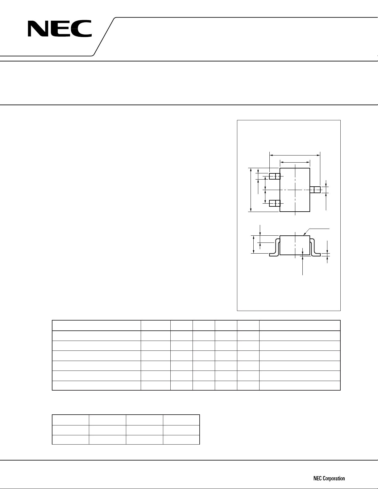
PACKAGE DIMENSIONS
in millimeters
2.1 ± 0.1
1.25 ± 0.1
2
0.65
+0.1
–0
0.3
2.0 ± 0.2
0.65
1
3
+0.1
–0
0.3
ABSOLUTE MAXIMUM RATINGS (TA = 25 ˚C)
Collector to Base Voltage VCB0 30 V
Collector to Emitter Voltage V
Emitter to Base Voltage V
Collector Current I
Total Power Dissipation P
Junction Temperature T
Storage Temperature T
CE0 15 V
EB0 4.0 V
C 50 mA
T 160 mW
j 150 ˚C
stg –65 to +150 ˚C
0.3
0.9 ± 0.1
PIN CONNECTIONS
1. Emitter
2. Base
3. Collector
Marking
0 to 0.1
ELECTRICAL CHARACTERISTICS (TA = 25 ˚C)
Characteristics Symbol MIN. TYP. MAX. Unit Test Conditions
Collector Cutoff Current ICB0 0.1
DC Current Gain hFE 40 100 200 VCE = 3 V, IC = 5 mA
Collector Saturation Voltage
Gain Bandwidth Product fT 1.2 1.8 GHz VCE = 3 V, IC = 5 mA
Feedback Capacitance Cre 0.55 1.2 pF VCB = 3 V, IE = 0, f = 1 MHz
Collector to Base Time Constant CC ·rb’b 3.5 8.0 ps
VCE(sat) 0.5 V
µ
AVCB = 20 V, IE = 0
IC = 10 mA, IB = 1 mA
VCE = 3 V, IE = –5 mA, f = 31.9 MHz
+0.1
0.15
–0.05
hFE Classifications
Rank T42 T43 T44
Marking T42 T43 T44
hFE 40 to 80 60 to 120 100 to 200
Document No. P11189EJ2V0DS00 (2nd edition)
(Previous No. TP-2253)
Date Published February 1996 P
Printed in Japan
©
1996
Page 2
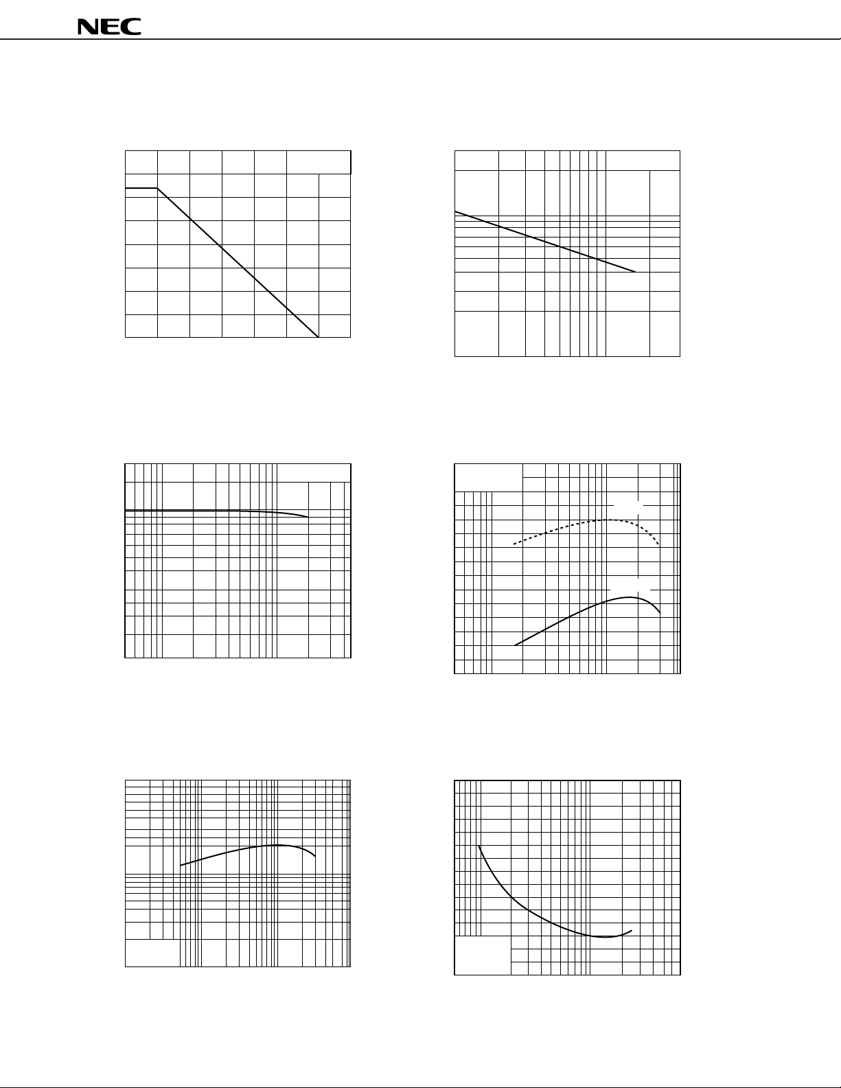
TYPICAL CHARACTERISTICS (TA = 25 ˚C)
2SC4184
TOTAL POWER DISSIPATION vs.
AMBIENT TEMPERATURE
200
150
100
50
- Total Power Dissipation - W
T
P
0
50 100 150
TA - Ambient Temperature - ˚C
DC CURRENT GAIN vs.
COLLECTOR CURRENT
200
100
Free Air
VCE = 10 V
TYPICAL DEVICE CAPACITANCE vs.
COLLECTOR TO BASE VOLTAGE
3
2
1
0.7
0.5
0.3
- Feed-back Capacitance - pF
0.2
re
C
0.1
CB
- Collector to Base Voltage - V
V
71
INSERTION GAIN, MAXIMUM AVAILABLE
GAIN vs. COLLECTOR CURRENT
15
VCE = 10 V
f = 1.0 GHz
f = 1.0 MHz
201053230
MAG
50
- DC Current Gain
FE
h
20
10
0.5
I
C
- Collector Current - mA
511050
GAIN BANDWIDTH PRODUCT vs.
COLLECTOR CURRENT
10
5.0
3.0
2.0
1.0
0.5
0.3
0.2
- Gain Bandwidth Product - MHz
VCE = 10 V
T
f
0.1
0.1
I
C
- Collector Current - mA
10
2
S
21e
- Insertion Gain - dB
5
2
21e
- Maximum Available Gain - dB
S
max
G
0
0.5 1
510
I
C
- Collector Current - mA
50
70
COLLECTOR TO BASE TIME
CONSTANT vs. COLLECTOR CURRENT
15
10
5
VCE = 10 V
- Collector to Base Time Constant - ps
b
f = 31.9 MHz
·
b
0
100.5
305.01.0
·r
C
C
0.5 50101
5
I
C
- Collector Current - mA
70
2
Page 3

S-PARAMETER
VCE = 3 V, IC = 3 mA
Frequency S11 S21 S12 S22
MHz MAG ANG MAG ANG MAG ANG MAG ANG
100.00 0.780 –45.1 7.990 142.7 0.038 72.2 0.912 –14.1
200.00 0.599 –75.4 5.939 120.0 0.055 58.9 0.787 –18.6
300.00 0.461 –97.5 4.471 104.5 0.070 52.2 0.702 –21.4
400.00 0.389 –113.6 3.554 95.7 0.079 54.5 0.666 –20.8
500.00 0.349 –127.2 3.002 88.2 0.087 54.5 0.625 –20.8
600.00 0.327 –140.4 2.590 83.5 0.098 57.4 0.623 –21.4
700.00 0.311 –152.0 2.301 76.2 0.107 56.8 0.613 –21.7
800.00 0.304 –161.4 2.086 71.6 0.121 57.7 0.617 –24.0
900.00 0.303 –169.1 1.845 66.3 0.128 59.5 0.616 –26.0
1000.00 0.315 –176.4 1.697 61.8 0.139 58.7 0.604 –29.8
1100.00 0.329 175.8 1.567 58.5 0.149 60.7 0.595 –32.6
1200.00 0.335 167.5 1.480 53.8 0.160 60.3 0.575 –35.2
1300.00 0.337 161.8 1.412 49.6 0.175 60.1 0.561 –37.4
1400.00 0.341 157.7 1.294 45.5 0.179 60.2 0.548 –39.5
1500.00 0.359 154.0 1.215 40.5 0.192 59.0 0.547 –41.9
1600.00 0.378 150.3 1.144 39.9 0.200 62.0 0.541 –45.1
1700.00 0.395 144.9 1.071 37.1 0.212 61.2 0.535 –48.8
1800.00 0.412 140.7 1.065 35.3 0.230 62.8 0.524 –52.9
1900.00 0.421 137.4 1.028 32.3 0.246 61.8 0.515 –56.6
2000.00 0.436 134.3 1.018 27.4 0.263 59.6 0.502 –60.5
2SC4184
V
CE = 3 V, IC = 10 mA
Frequency S11 S21 S12 S22
MHz MAG ANG MAG ANG MAG ANG MAG ANG
100.00 0.471 –83.2 13.160 120.4 0.026 64.3 0.757 –17.7
200.00 0.349 –119.5 7.654 100.5 0.037 63.0 0.646 –16.0
300.00 0.301 –140.2 5.293 89.6 0.050 63.2 0.605 –16.1
400.00 0.291 –153.2 3.997 83.3 0.061 67.1 0.592 –15.5
500.00 0.295 –163.3 3.219 77.5 0.072 66.9 0.572 –15.5
600.00 0.301 –172.5 2.829 74.7 0.085 69.9 0.579 –16.5
700.00 0.306 179.5 2.483 68.7 0.096 68.7 0.577 –17.1
800.00 0.313 174.1 2.232 64.8 0.111 68.7 0.584 –19.8
900.00 0.323 169.9 1.961 60.5 0.120 70.1 0.587 –22.1
1000.00 0.346 165.4 1.794 56.7 0.132 68.4 0.577 –26.1
1100.00 0.370 160.2 1.652 53.9 0.144 70.0 0.570 –29.0
1200.00 0.380 153.6 1.552 49.4 0.153 69.0 0.552 –31.9
1300.00 0.386 149.0 1.479 45.4 0.170 69.0 0.540 –34.2
1400.00 0.391 146.0 1.346 41.8 0.177 69.0 0.529 –36.5
1500.00 0.410 143.2 1.259 36.9 0.191 67.6 0.529 –39.1
1600.00 0.430 140.6 1.181 36.5 0.201 70.2 0.523 –42.4
1700.00 0.448 136.2 1.100 34.0 0.215 69.1 0.520 –46.2
1800.00 0.466 132.8 1.094 32.5 0.236 70.4 0.509 –50.6
1900.00 0.475 129.9 1.047 29.7 0.253 68.8 0.499 –54.5
2000.00 0.490 127.0 1.034 24.9 0.273 66.3 0.487 –58.6
3
Page 4

VCE = 5 V, IC = 3 mA
Frequency S11 S21 S12 S22
MHz MAG ANG MAG ANG MAG ANG MAG ANG
100.00 0.787 –43.0 8.019 143.8 0.035 70.1 0.923 –12.5
200.00 0.606 –72.3 6.026 121.4 0.051 60.3 0.810 –16.8
300.00 0.465 –93.7 4.568 105.8 0.065 54.3 0.729 –19.4
400.00 0.389 –109.3 3.640 97.1 0.073 56.6 0.695 –18.9
500.00 0.345 –122.8 3.081 89.6 0.080 55.6 0.656 –18.8
600.00 0.320 –136.0 2.658 84.8 0.091 58.7 0.656 –19.4
700.00 0.302 –147.7 2.367 77.6 0.099 58.1 0.647 –19.6
800.00 0.294 –157.5 2.144 73.1 0.112 59.3 0.653 –22.0
900.00 0.291 –165.6 1.897 67.7 0.119 61.4 0.653 –23.7
1000.00 0.301 –173.4 1.743 63.4 0.130 60.8 0.641 –27.4
1100.00 0.313 178.4 1.610 60.2 0.139 62.8 0.633 –29.9
1200.00 0.319 170.0 1.520 55.3 0.149 62.3 0.612 –32.4
1300.00 0.320 164.0 1.447 51.3 0.164 62.4 0.599 –34.4
1400.00 0.324 159.7 1.326 47.2 0.168 62.6 0.587 –36.3
1500.00 0.343 155.9 1.244 42.4 0.181 61.8 0.586 –38.3
1600.00 0.363 151.9 1.172 41.6 0.187 64.8 0.581 –41.1
1700.00 0.379 146.5 1.100 38.9 0.200 64.2 0.579 –44.7
1800.00 0.396 142.2 1.095 37.0 0.216 65.9 0.568 –48.3
1900.00 0.406 138.7 1.054 34.0 0.233 65.1 0.560 –51.7
2000.00 0.421 135.5 1.043 29.1 0.250 63.0 0.547 –55.3
2SC4184
V
CE = 5 V, IC = 10 mA
Frequency S11 S21 S12 S22
MHz MAG ANG MAG ANG MAG ANG MAG ANG
100.00 0.487 –77.7 13.538 122.2 0.024 64.1 0.785 –16.2
200.00 0.346 –113.2 8.008 101.9 0.035 63.2 0.681 –14.7
300.00 0.290 –134.4 5.559 90.9 0.048 63.6 0.638 –14.8
400.00 0.275 –148.3 4.216 84.6 0.057 67.6 0.626 –14.1
500.00 0.275 –158.7 3.396 78.8 0.067 68.0 0.606 –14.1
600.00 0.280 –168.6 2.974 76.0 0.080 70.5 0.613 –15.0
700.00 0.284 –176.9 2.610 70.2 0.090 69.6 0.612 –15.5
800.00 0.291 177.1 2.347 66.4 0.104 70.0 0.620 –17.9
900.00 0.302 172.6 2.065 62.0 0.112 71.2 0.625 –20.1
1000.00 0.324 167.8 1.884 58.2 0.124 69.8 0.616 –23.9
1100.00 0.346 162.2 1.734 55.5 0.134 71.3 0.608 –26.5
1200.00 0.358 155.4 1.630 51.2 0.143 70.7 0.590 –29.1
1300.00 0.364 150.7 1.548 47.3 0.159 71.0 0.579 –31.1
1400.00 0.369 147.6 1.410 43.7 0.165 71.1 0.568 –33.0
1500.00 0.389 144.8 1.320 38.9 0.179 70.0 0.569 –35.2
1600.00 0.408 142.0 1.236 38.5 0.189 72.6 0.564 –38.1
1700.00 0.427 137.5 1.153 35.9 0.203 71.5 0.563 –41.8
1800.00 0.445 134.0 1.147 34.3 0.222 73.1 0.553 –45.6
1900.00 0.455 131.1 1.102 31.7 0.238 71.7 0.545 –49.1
2000.00 0.470 128.3 1.089 26.5 0.258 69.2 0.533 –52.9
4
Page 5

VCE = 10 V, IC = 3 mA
Frequency S11 S21 S12 S22
MHz MAG ANG MAG ANG MAG ANG MAG ANG
100.00 0.799 –40.5 7.976 145.0 0.030 71.8 0.937 –10.9
200.00 0.618 –68.1 6.066 122.9 0.046 60.5 0.836 –14.6
300.00 0.471 –88.5 4.643 107.4 0.057 56.0 0.763 –17.0
400.00 0.390 –103.5 3.710 98.6 0.065 57.7 0.733 –16.5
500.00 0.340 –116.4 3.144 91.1 0.073 57.3 0.695 –16.5
600.00 0.311 –129.5 2.719 86.4 0.083 60.3 0.698 –17.0
700.00 0.290 –141.4 2.419 79.2 0.090 60.1 0.690 –17.0
800.00 0.278 –151.6 2.194 74.7 0.103 61.0 0.698 –19.3
900.00 0.273 –160.3 1.941 69.4 0.108 63.5 0.699 –20.8
1000.00 0.280 –168.7 1.782 65.1 0.118 62.7 0.689 –24.4
1100.00 0.291 –177.4 1.644 61.8 0.127 65.1 0.679 –26.7
1200.00 0.296 173.6 1.551 57.0 0.136 64.9 0.657 –28.9
1300.00 0.298 167.4 1.474 53.0 0.149 65.0 0.646 –30.4
1400.00 0.302 162.8 1.350 49.0 0.153 65.7 0.633 –32.0
1500.00 0.321 158.6 1.269 44.3 0.165 65.0 0.637 –33.7
1600.00 0.340 154.4 1.197 43.5 0.172 67.9 0.631 –36.1
1700.00 0.357 148.7 1.124 40.9 0.184 67.7 0.632 –39.3
1800.00 0.374 144.1 1.117 39.1 0.201 69.6 0.624 –42.5
1900.00 0.385 140.4 1.077 36.0 0.214 68.9 0.616 –45.6
2000.00 0.399 137.1 1.064 31.0 0.230 66.7 0.606 –48.7
2SC4184
V
CE = 10 V, IC = 10 mA
Frequency S11 S21 S12 S22
MHz MAG ANG MAG ANG MAG ANG MAG ANG
100.00 0.507 –71.4 13.698 124.2 0.022 69.9 0.816 –14.2
200.00 0.348 –104.2 8.229 103.6 0.032 65.4 0.719 –13.1
300.00 0.279 –124.9 5.731 92.4 0.044 64.5 0.678 –13.3
400.00 0.254 –139.4 4.348 86.2 0.054 68.8 0.669 –12.6
500.00 0.249 –150.8 3.504 80.2 0.062 68.1 0.647 –12.5
600.00 0.251 –161.6 3.083 77.6 0.074 71.4 0.657 –13.3
700.00 0.254 –170.8 2.710 71.8 0.083 70.4 0.656 –13.6
800.00 0.261 –177.6 2.436 68.1 0.096 70.8 0.665 –15.9
900.00 0.271 177.0 2.141 63.7 0.103 72.0 0.669 –17.8
1000.00 0.292 171.7 1.953 60.0 0.114 70.8 0.661 –21.4
1100.00 0.314 165.4 1.798 57.3 0.123 72.8 0.654 –23.7
1200.00 0.324 158.4 1.691 52.9 0.132 72.2 0.634 –26.0
1300.00 0.332 153.5 1.604 49.1 0.147 72.8 0.625 –27.7
1400.00 0.338 150.0 1.461 45.6 0.151 72.8 0.613 –29.3
1500.00 0.358 147.1 1.369 40.9 0.165 72.1 0.618 –30.9
1600.00 0.378 144.0 1.282 40.4 0.174 75.1 0.613 –33.4
1700.00 0.397 139.5 1.201 38.0 0.187 74.3 0.615 –36.7
1800.00 0.415 135.8 1.188 36.4 0.205 75.8 0.607 –39.8
1900.00 0.426 132.7 1.147 33.4 0.219 74.6 0.599 –43.1
2000.00 0.442 129.9 1.130 28.6 0.238 72.4 0.589 –46.4
5
Page 6

2SC4184
No part of this document may be copied or reproduced in any form or by any means without the prior written
consent of NEC Corporation. NEC Corporation assumes no responsibility for any errors which may appear in this
document.
NEC Corporation does not assume any liability for infringement of patents, copyrights or other intellectual
property rights of third parties by or arising from use of a device described herein or any other liability arising
from use of such device. No license, either express, implied or otherwise, is granted under any patents,
copyrights or other intellectual property rights of NEC Corporation or others.
While NEC Corporation has been making continuous effort to enhance the reliability of its semiconductor devices,
the possibility of defects cannot be eliminated entirely. To minimize risks of damage or injury to persons or
property arising from a defect in an NEC semiconductor device, customer must incorporate sufficient safety
measures in its design, such as redundancy, fire-containment, and anti-failure features.
NEC devices are classified into the following three quality grades:
“Standard“, “Special“, and “Specific“. The Specific quality grade applies only to devices developed based on
a customer designated “quality assurance program“ for a specific application. The recommended applications
of a device depend on its quality grade, as indicated below. Customers must check the quality grade of each
device before using it in a particular application.
Standard: Computers, office equipment, communications equipment, test and measurement equipment,
audio and visual equipment, home electronic appliances, machine tools, personal electronic
equipment and industrial robots
Special: Transportation equipment (automobiles, trains, ships, etc.), traffic control systems, anti-disaster
systems, anti-crime systems, safety equipment and medical equipment (not specifically designed
for life support)
Specific: Aircrafts, aerospace equipment, submersible repeaters, nuclear reactor control systems, life
support systems or medical equipment for life support, etc.
The quality grade of NEC devices in “Standard“ unless otherwise specified in NEC's Data Sheets or Data Books.
If customers intend to use NEC devices for applications other than those specified for Standard quality grade,
they should contact NEC Sales Representative in advance.
Anti-radioactive design is not implemented in this product.
M4 94.11
6
 Loading...